Lab 4 - EE 421L Fall 2020 

Authored by Xianjie Cao

15 September 2020


Pre-lab:

    For our Pre-lab work, we supposed to layout and simulating the IV curves of PMOS and NMOS devices.


Three terminals NMOS symbol with its shematic:

http://cmosedu.com/jbaker/courses/ee421L/f20/students/caox2/Lab4/pre_01.png    http://cmosedu.com/jbaker/courses/ee421L/f20/students/caox2/Lab4/pre_02.png


The circuit built from the NMOS device and its IV characteristics:


http://cmosedu.com/jbaker/courses/ee421L/f20/students/caox2/Lab4/pre_03.png    http://cmosedu.com/jbaker/courses/ee421L/f20/students/caox2/Lab4/pre_04.png


The Extract view of the circuit tells us that the  symbol has 4 terminals, that's because when a 3 terminal MOSFET symbol is used, it's assumed that the bulk is connected to the gnd! for NMOS and to VDD! for PMOS. 

http://cmosedu.com/jbaker/courses/ee421L/f20/students/caox2/Lab4/pre_14.png


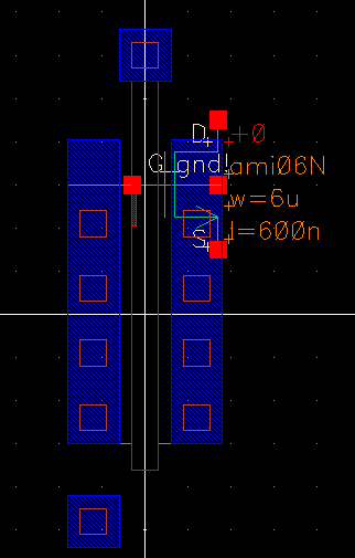
To fix that we'll ave to remove the metal1 rectangle and pin connecting the S to thhe bulk, as seen below:

http://cmosedu.com/jbaker/courses/ee421L/f20/students/caox2/Lab4/pre_05.png


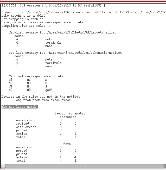
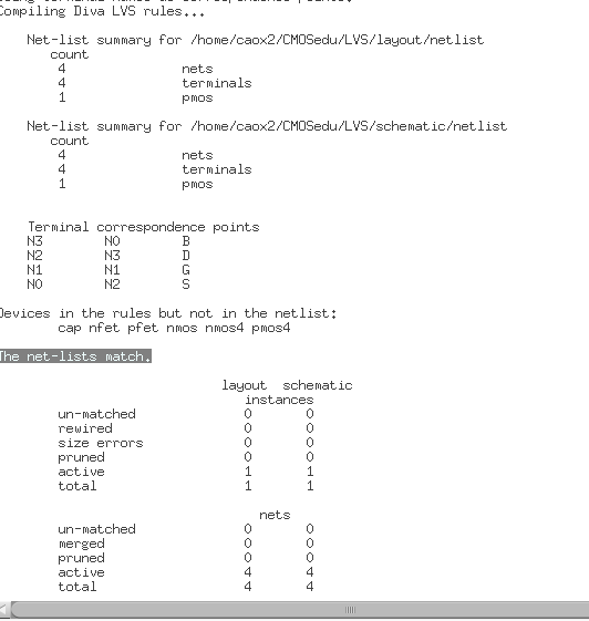
In order to run the LVS, there is one more step left, we need to change the cell name in the schematic from nmos to nmos4. After that, the LVS output is as following:

http://cmosedu.com/jbaker/courses/ee421L/f20/students/caox2/Lab4/pre_15.png

http://cmosedu.com/jbaker/courses/ee421L/f20/students/caox2/Lab4/pre_06.png


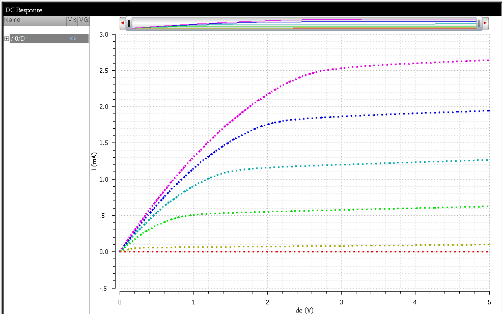
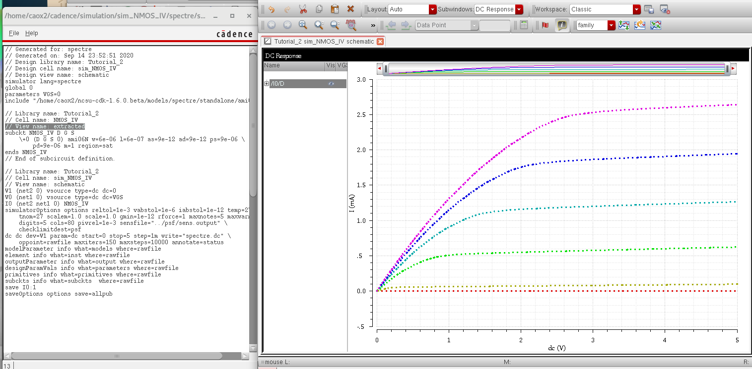
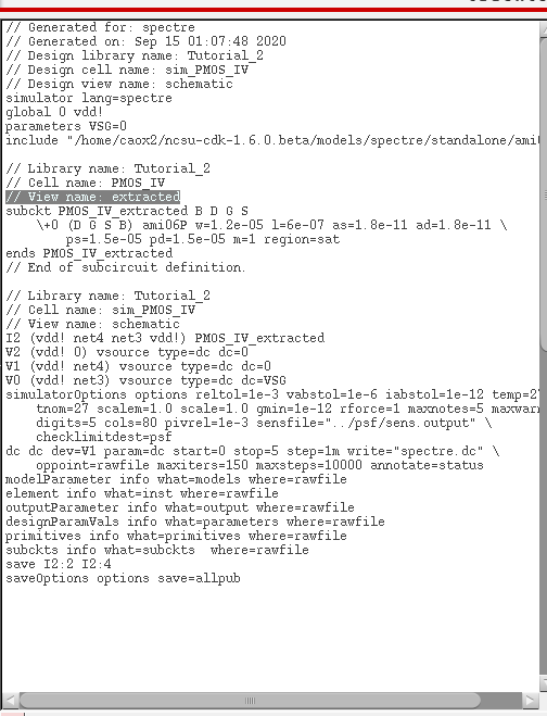
Then we simulate the extracted layout:


http://cmosedu.com/jbaker/courses/ee421L/f20/students/caox2/Lab4/pre_07.png


After finishing the NMOS, We need to do almost identical procedures for PMOS.
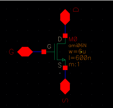
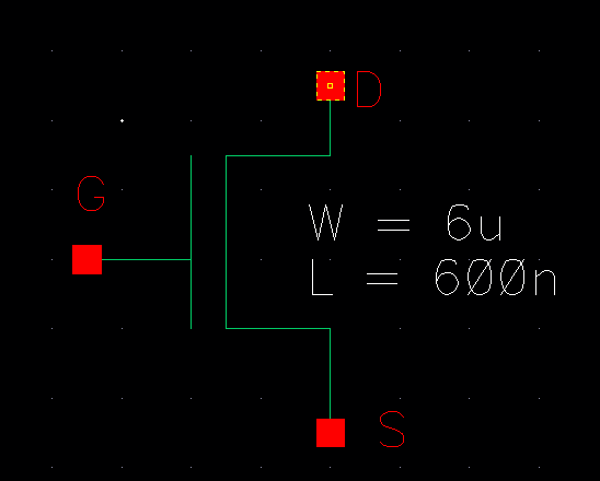
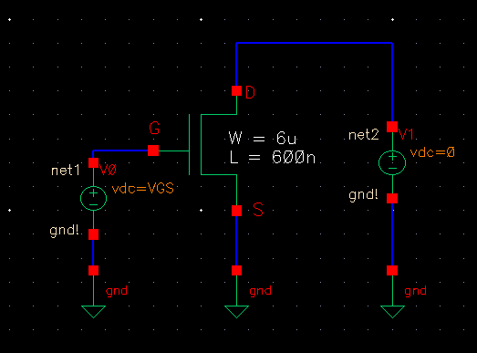
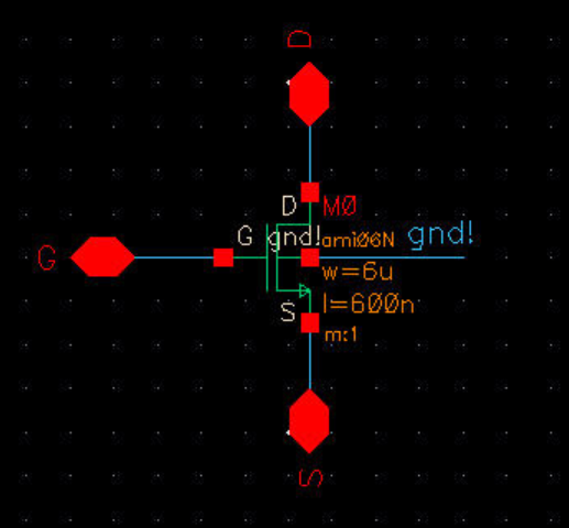
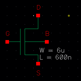
The shematic and the symbol view are seen below:

http://cmosedu.com/jbaker/courses/ee421L/f20/students/caox2/Lab4/pre_08.png    http://cmosedu.com/jbaker/courses/ee421L/f20/students/caox2/Lab4/pre_09.png


Layout for the PMOS:

http://cmosedu.com/jbaker/courses/ee421L/f20/students/caox2/Lab4/pre_10.png


Extract view of the layout:

http://cmosedu.com/jbaker/courses/ee421L/f20/students/caox2/Lab4/pre_13.png

Circuit designed to show the IV characteristic for the PMOS:

http://cmosedu.com/jbaker/courses/ee421L/f20/students/caox2/Lab4/pre_16.png


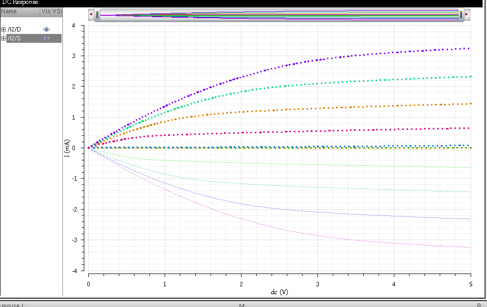
Extracted simulation:

http://cmosedu.com/jbaker/courses/ee421L/f20/students/caox2/Lab4/pre_12.png    

http://cmosedu.com/jbaker/courses/ee421L/f20/students/caox2/Lab4/pre_11.png


Lab description

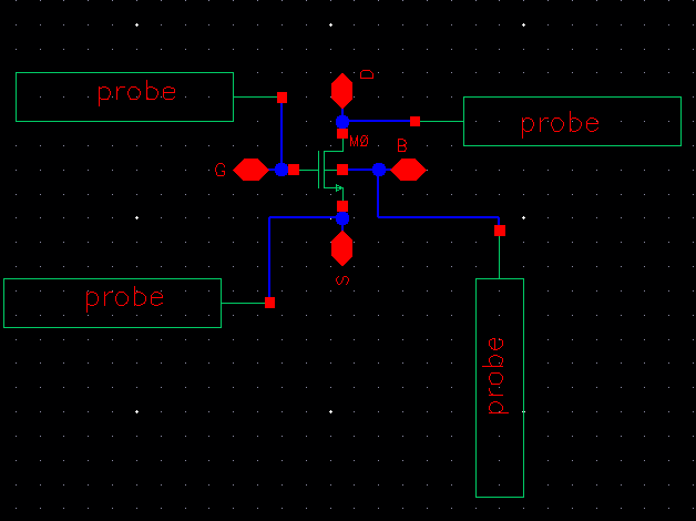
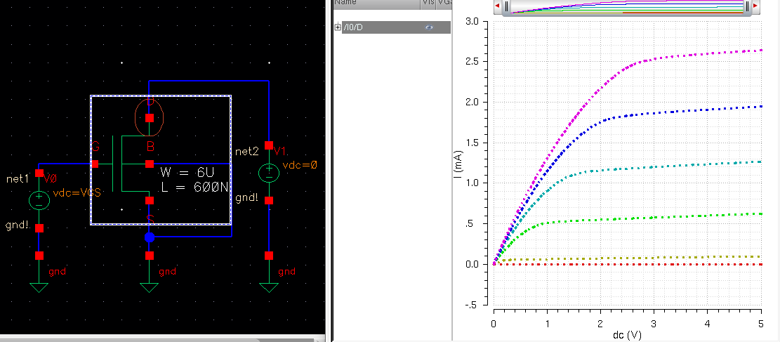
        1. A schematic for simulating ID v. VDS of an NMOS device for VGS varying from 0 to 5 V in 1 V steps while VDS varies from 0 to 5 V in 1 mV steps. Use a 6u/600n width-to-length ratio.

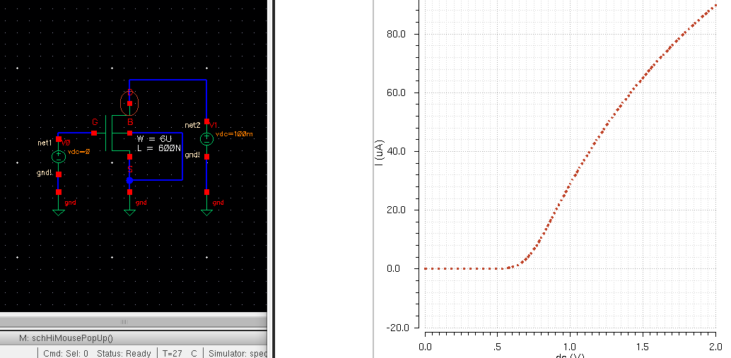
        2. A schematic for simulating ID v. VGS of an NMOS device for VDS = 100 mV where VGS varies from 0 to 2 V in 1 mV steps. Again use a 6u/600n width-to-length ratio. 

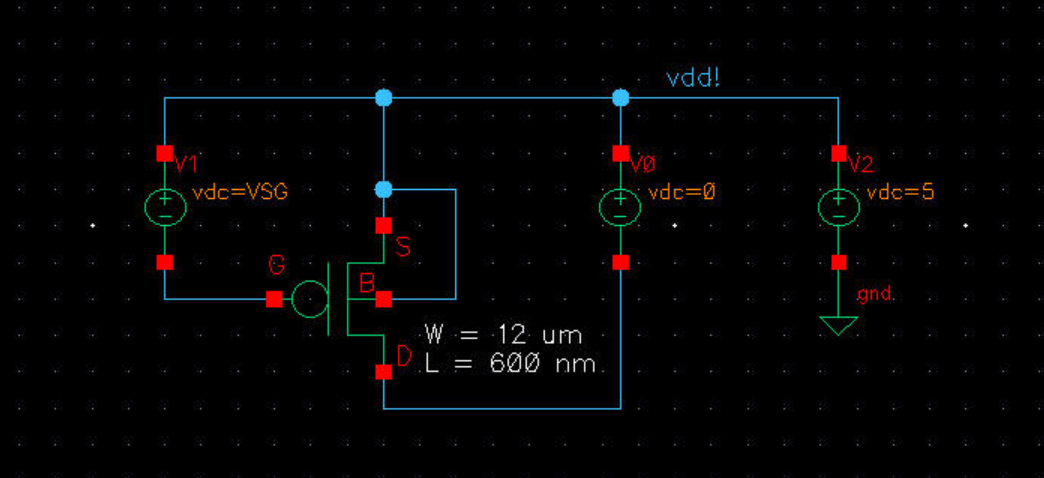
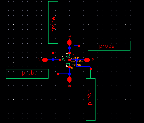
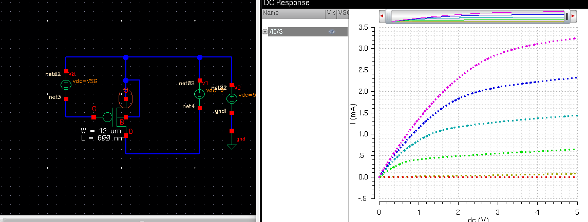
       3. A schematic for simulating ID v. VSD (note VSD not VDS) of a PMOS device for VSG (not VGS) varying from 0 to 5 V in 1 
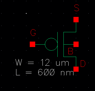
V steps while VSD varies from 0 to 5 V in 1 mV steps. Use a 12u/600n width-to-length ratio.

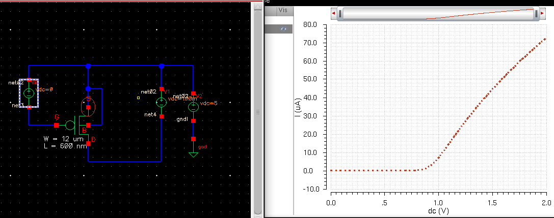
        4. A schematic for simulating ID v. VSG of a PMOS device for VSD = 100 mV where VSG varies from 0 to 2 V in 1 mV steps. Again, use a 12u/600n width-to-length ratio. 

Lab procedure:

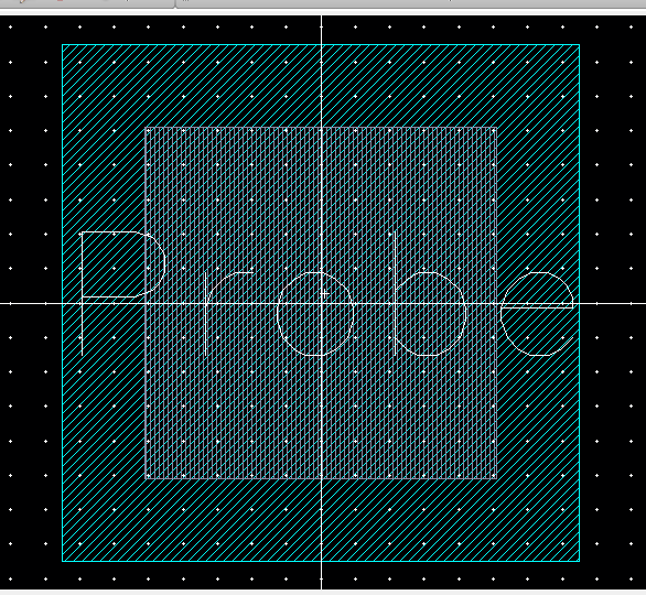
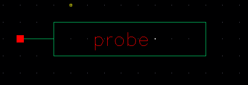
    1) Lay out the Probe pad with metal3 and glass layer, then create a symbol for it.

http://cmosedu.com/jbaker/courses/ee421L/f20/students/caox2/Lab4/snip_01.png    http://cmosedu.com/jbaker/courses/ee421L/f20/students/caox2/Lab4/snip_02.png


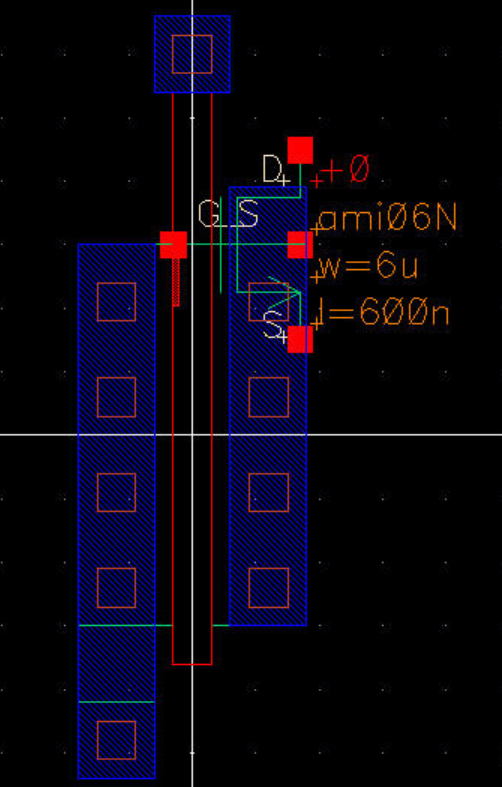
    2) Draw the schematic for a 4 terminals NMOS device and then create a symbol from the cellview.

http://cmosedu.com/jbaker/courses/ee421L/f20/students/caox2/Lab4/snip_04.png    http://cmosedu.com/jbaker/courses/ee421L/f20/students/caox2/Lab4/snip_03.png 


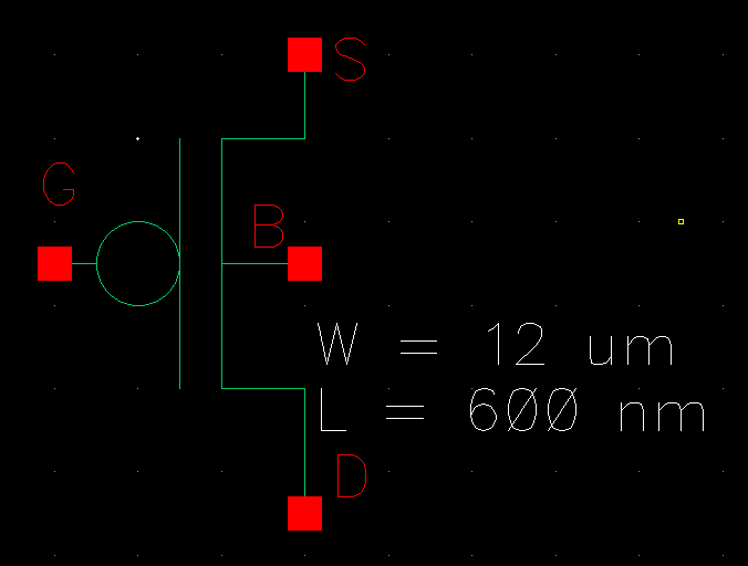
    3) Schematic for a 4 terminals PMOS device and its symbol.

http://cmosedu.com/jbaker/courses/ee421L/f20/students/caox2/Lab4/snip_06.png    http://cmosedu.com/jbaker/courses/ee421L/f20/students/caox2/Lab4/snip_05.png


    4) Simulation of ID vs VDS of an NMOS devices for VGS varying from 0 to 5V in 1V steps while VDS varies from 0 to 5V in 1mV steps.

http://cmosedu.com/jbaker/courses/ee421L/f20/students/caox2/Lab4/snip_07.png


    5) Simulation of ID vs VGS of an NMOS device for VDS = 100mV and VGS varies from 0 to 2V in 1 mV steps.

http://cmosedu.com/jbaker/courses/ee421L/f20/students/caox2/Lab4/snip_08.png


    6) Simulation of ID vs VSD of a PMOS device for VSG varying from 0 to 5 V in 1V steps and VSD varies from 0 to 5V in 1mV steps.

http://cmosedu.com/jbaker/courses/ee421L/f20/students/caox2/Lab4/snip_09.png


    7) Simulation of ID vs VSG of a PMOS device for VSD = 100mV and VSG varies from 0 to 2V in 1mV steps.

 http://cmosedu.com/jbaker/courses/ee421L/f20/students/caox2/Lab4/snip_10.png


    8) Layout of the NMOS device with all 4 terminals connecting to probe pads.

http://cmosedu.com/jbaker/courses/ee421L/f20/students/caox2/Lab4/snip_12.png


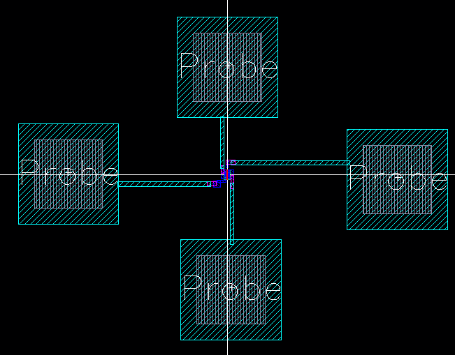
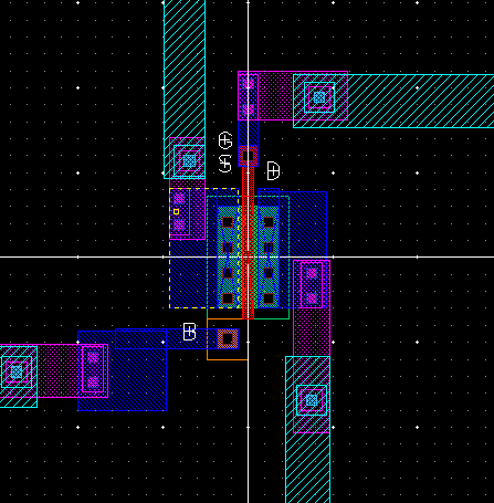
The closer view of the layer connections.

http://cmosedu.com/jbaker/courses/ee421L/f20/students/caox2/Lab4/snip_13.png


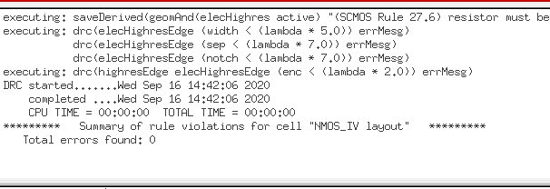
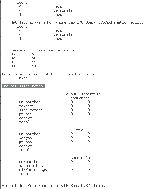
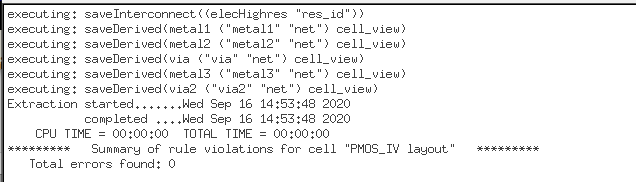
Passed both DRC and LVS check.

http://cmosedu.com/jbaker/courses/ee421L/f20/students/caox2/Lab4/snip_11.png    

http://cmosedu.com/jbaker/courses/ee421L/f20/students/caox2/Lab4/snip_14.png


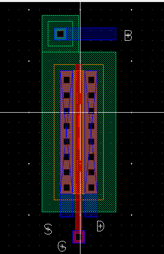
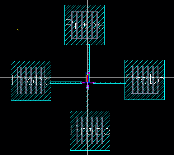
    9) Layout of the PMOS device with all 4 terminals connecting to probe pads.

 http://cmosedu.com/jbaker/courses/ee421L/f20/students/caox2/Lab4/snip_17.png


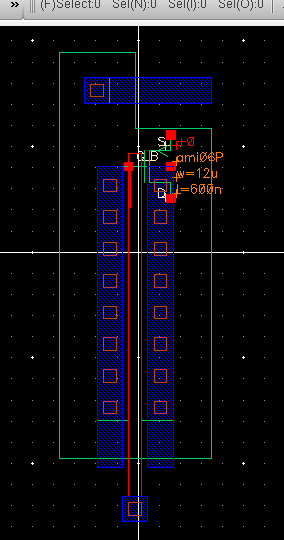
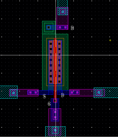
Closer view of the layer connections.

http://cmosedu.com/jbaker/courses/ee421L/f20/students/caox2/Lab4/snip_16.png


Passed both DRC and LVS.

http://cmosedu.com/jbaker/courses/ee421L/f20/students/caox2/Lab4/snip_15.png

http://cmosedu.com/jbaker/courses/ee421L/f20/students/caox2/Lab4/snip_18.png


Backups:

    zipped the library folder and the folder that has all the collected images to the desktop, then upload them into my personal github repository for backups.

http://cmosedu.com/jbaker/courses/ee421L/f20/students/caox2/Lab4/snip_19.png    http://cmosedu.com/jbaker/courses/ee421L/f20/students/caox2/Lab4/snip_20.png


Return to EE421L Labs