Lab 3 - EE421L Fall 2020
Authored
by Xianjie Cao
7 September 2020
Pre-lab:
For
our Pre-lab work, We supposed to back-up all the previous work from
lab, and finish Tutorial 1 that demonstrates how to lay-out a n-well
resistor.
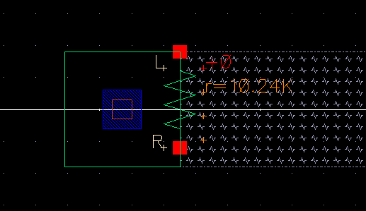
The lay-out and extracted of the 10K n-well resistor:


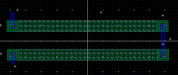
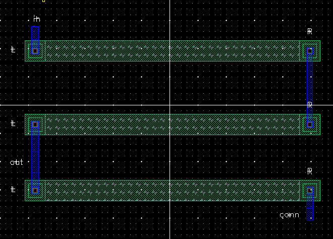
The lay-out of the voltage divider:

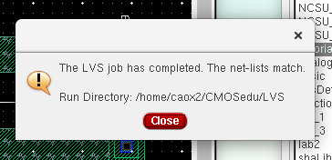
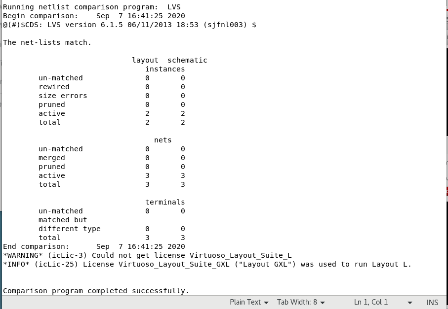
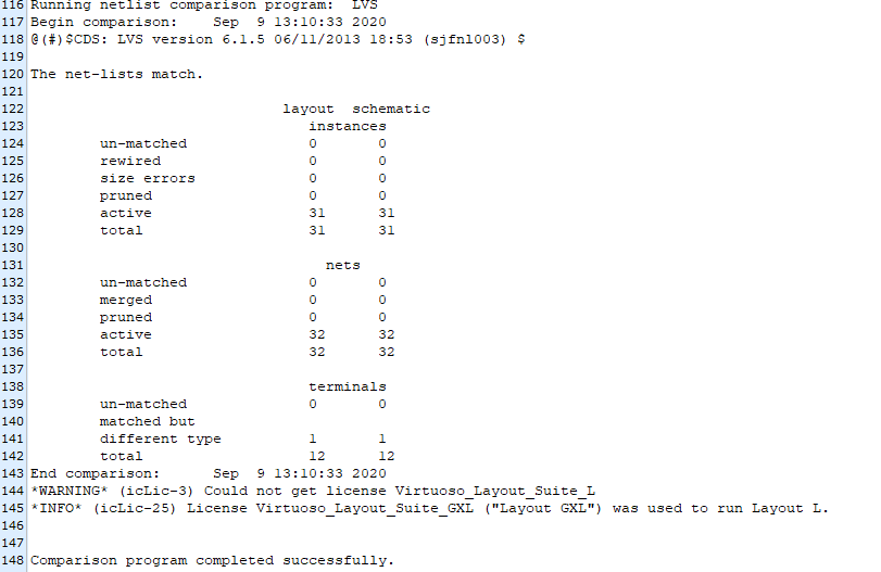
The LVS result showing that net-lists match:


Lab
description
The
Lab focuses on how to layout the 10-bit DAC that we designed in the
Lab2, and how to make sure the layout passes DRC and LVS verification.
Lab procedure:1) Use
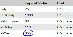
the n-well to layout a 10K resistor. To determine the width, we can
refer to the following pictures, for C5 process, lambda is 0.30um,
and withde is 12 * lambda, which is 12 * 0.30um gives us
3.6um for the width. The sheet resistance for n-well is 855, hence,
length can be calculated using L = R/R_sheet * width, for our case, L =
10K/855*3.6um, approximately, it gives us 42um. For the sake of
simulation, we can choose 45um as our length.


The layout is as shown:

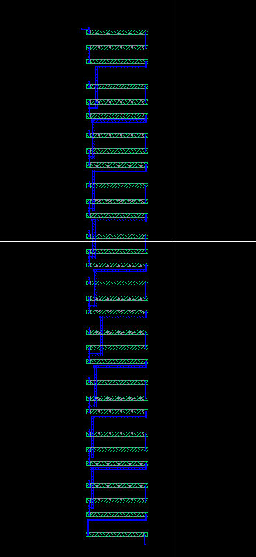
2) Use the resistor layout to layout DAC.

3) The design passed the DRC and LVS check. (Images showing with no error and net-listst match).


Backups:
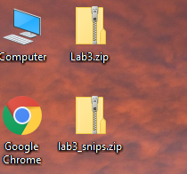
zipped
the library folder and the folder that has all the collected images to
the desktop, then upload them into my personal github repository for
backups.


Return to EE421L Labs

