Lab 2 - EE 421L Fall 2020

Authored by Xiannjie Cao   

1 September 2020


Pre-lab:

     For the pre-lab work,  download the lab2.zip folder from CMOSedu website, which it contains a circuit using an ideal 10-bit ADC and a 10-bit DAC. Run a transient response for the circuit, to understand the relationship between the input voltage, Vin with B[9:0] bus and Vout.


 http://cmosedu.com/jbaker/courses/ee421L/f20/students/caox2/Lab2/snap_1.png


The schematic is as following:


http://cmosedu.com/jbaker/courses/ee421L/f20/students/caox2/Lab2/snap_2.png


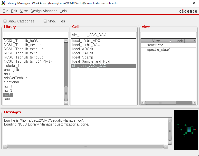
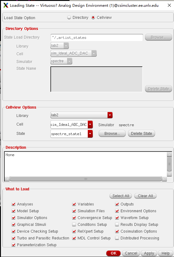
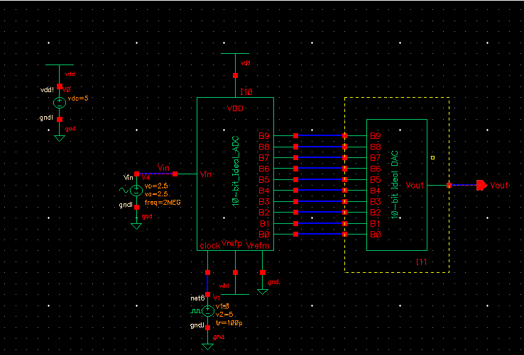
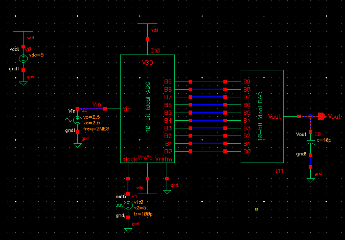
For the simulation purpose, we could just load the state from Cellview as it was given in the lab2.zip folder.


http://cmosedu.com/jbaker/courses/ee421L/f20/students/caox2/Lab2/snap_3.png               http://cmosedu.com/jbaker/courses/ee421L/f20/students/caox2/Lab2/snap_4.png

   
Since the input frequency is 2MEG Hz, 1 us will give us a graph of 2 periods.
   
http://cmosedu.com/jbaker/courses/ee421L/f20/students/caox2/Lab2/snap_5.png
   
From the simulation, we can conclude that the relationship between Vin and B[9:0] is that B[9:0] is the digital interpretation of the Vin through the 10-bit anoalog to digital converter, and the relationship between the Vin and Vout is that Vout is the DAC-processed of the Vin that has previously processed by a 10-bit ADC.

The LSB of the converter is given by http://cmosedu.com/jbaker/courses/ee421L/f20/students/caox2/Lab2/snap_7.png
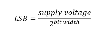
, in our case, bit width is 10, hence LSB = 5V/1024, which is approximately 4.88mV.
   
To better understand the ADC and the DAC, the following graph is obtained from a input voltage with DC offset 2.5V, amplitude 0.01V and frequency 2MEG Hz:
   
http://cmosedu.com/jbaker/courses/ee421L/f20/students/caox2/Lab2/snap_6.png
   
as we can see that first change is from 2.5 to 2.505V, therefore, LSB = 2.505- 2.5 = 5mV which is closer to our solution above.
   
Backups:
 
zipped the library folder and the folder that has all the collected images to the desktop, then upload them into my personal github repository for backups.
http://cmosedu.com/jbaker/courses/ee421L/f20/students/caox2/Lab2/snip_8.png        http://cmosedu.com/jbaker/courses/ee421L/f20/students/caox2/Lab2/snip_9.png


Lab description:

In this Lab, we'll replace the DAC from the pre-lab ADC-DAC circuit with our own designed DAC, which is implement by using 10k n-well resistors as seen below.


http://cmosedu.com/jbaker/courses/ee421L/f20/students/caox2/Lab2/snip_10.png


Lab procedure:

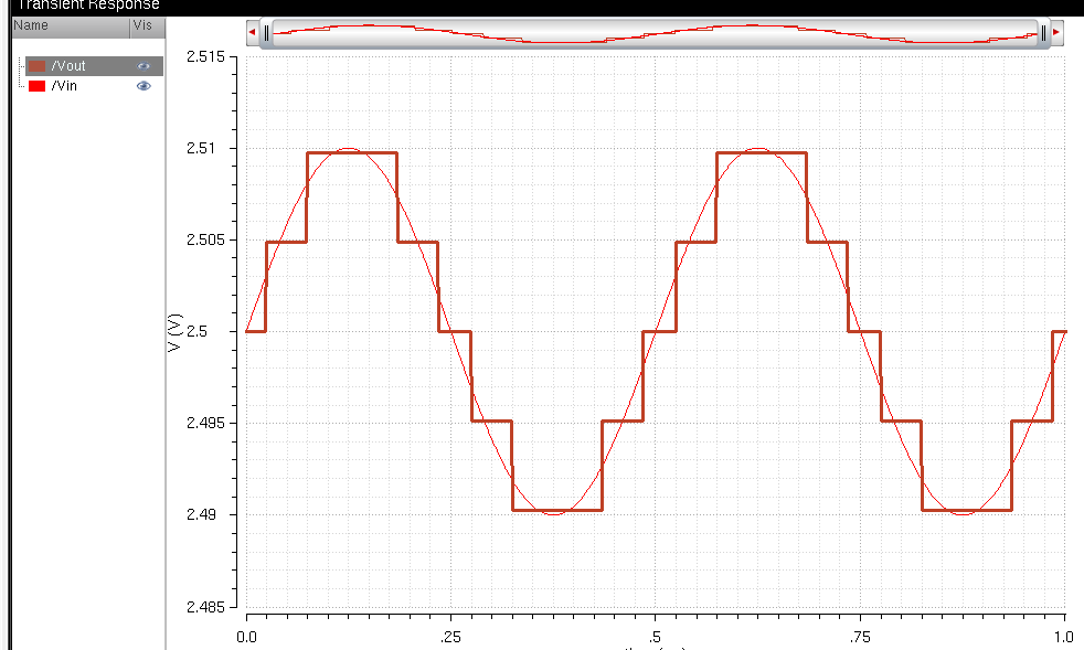
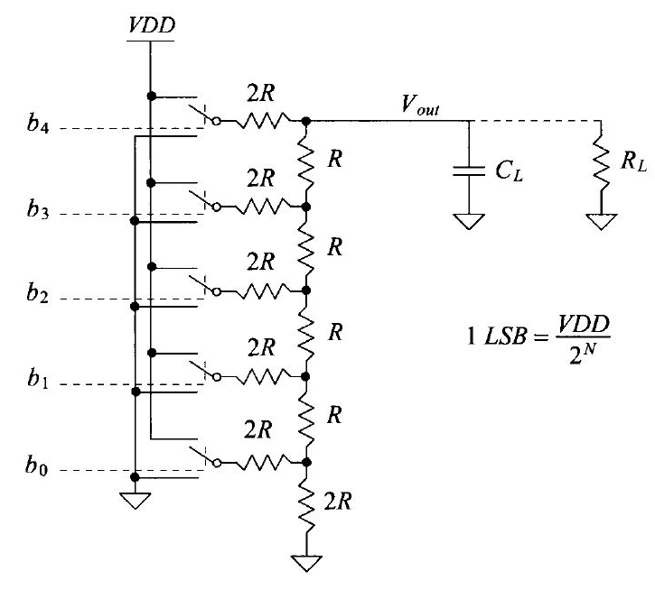
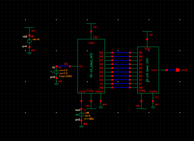
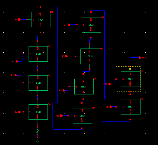
 1) As we saw from the above image, the controlling input bits are connect to a voltage divider; therefore, make a symbol for the voltage divider would be helpful.


http://cmosedu.com/jbaker/courses/ee421L/f20/students/caox2/Lab2/lab_snip_1.png         http://cmosedu.com/jbaker/courses/ee421L/f20/students/caox2/Lab2/lab_snip_2.png


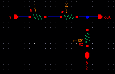
To determine the output resistance, we can combine the resistors, starting from very bottom, 2R || 2R which just R, then we add to the resistor in series, we now have 2R||2R again. By continue the same process, we will get the output resistance, in our case, just R (10K).


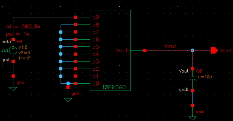
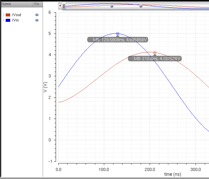
2) The Delay of thhe DAC when driving a 10 pF load can be calculated as 0.7RC, that is 0.7(10K)(10pF) = 70ns. To verify the correctness of the calculation, we can ground all DAC inputs, but with B9 connnnect to a pulse(0 to VDD). It should be as the following:


http://cmosedu.com/jbaker/courses/ee421L/f20/students/caox2/Lab2/snip_11.png    http://cmosedu.com/jbaker/courses/ee421L/f20/students/caox2/Lab2/snip_12.png


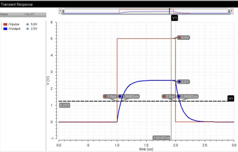
From the simulation, when Vout is at 1/2 of the maximum voltage, that is 1.25V, the delay is 1.069us - 1us = 69ns. Hence, delay verified. 


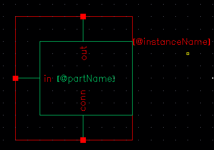
3) Creating our own symbol and schematic for the DAC.


http://cmosedu.com/jbaker/courses/ee421L/f20/students/caox2/Lab2/lab_snip_3.png    http://cmosedu.com/jbaker/courses/ee421L/f20/students/caox2/Lab2/lab_snip_4.png

4) To verify DAC functions correctly, we should simulate the DAC with different load.

Simulation under no load:


http://cmosedu.com/jbaker/courses/ee421L/f20/students/caox2/Lab2/lab_snip_5.png


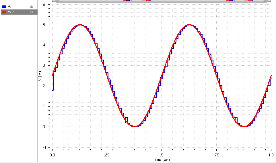
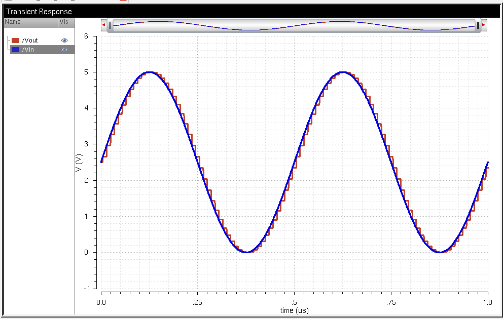
With no load, the Vout has the same amplitudes of the Vin, in fact, this is to be expected.


Simulation under 10K resistive load:


http://cmosedu.com/jbaker/courses/ee421L/f20/students/caox2/Lab2/lab_snip_6.png    http://cmosedu.com/jbaker/courses/ee421L/f20/students/caox2/Lab2/lab_snip_7.png


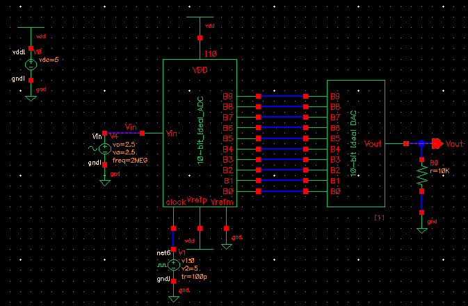
As we calculated at step 2, the output resistance is 10K when no load, hence, with the 10K resistive load, it forms a voltage divider, as result of this, Vout is going to be half of Vin.


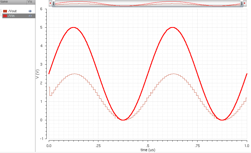
simulation under 10p capacitive load:


with the 10 pF caapacitor, it smooths the output waveform, but it also introduces the delay to the output.


simulation under 10K and 10pF load:

        http://cmosedu.com/jbaker/courses/ee421L/f20/students/caox2/Lab2/lab_snip_11.png
http://cmosedu.com/jbaker/courses/ee421L/f20/students/caox2/Lab2/lab_snip_10.png


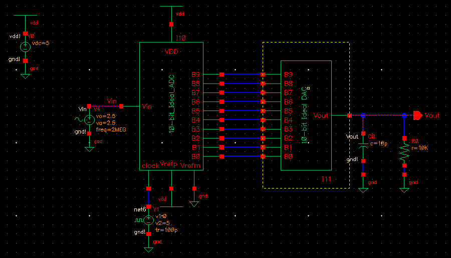
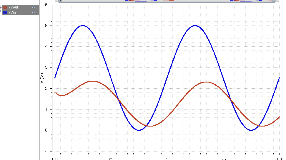
With both resistive and capacitive load, the output will still be lagging the input and half of the Vin amplitude.


5) Discuss what happens if the resistance of the switches isn't small compared to R.


If the switches' resistance isn't much smaller than R, then the output resistance of the DAC would be different, as result of this, it will affect the performance of the DAC.


Backups:

    zipped the library folder and the folder that has all the collected images to the desktop, then upload them into my personal github repository for backups.


Return to EE421L Labs