Lab 4: IV Characteristics and Layout of NMOS and PMOS Devices
EE 421L Digital Integrated Circuit Design
By Bryan Callaway- Email: callab2@unlv.nevada.edu
Last edited: 9/18/2020
Lab
description: In this lab we learned about laying out NMOS and PMOS
devices in ON's C5 process and obtaining the IV characteristic curves
for MOSFETs through simulation.
Prelab:
In the prelab, we laid out an NMOS and PMOS device in ON's C5 process.
For the NMOS, we started by laying out a design and creating a symbol for it:


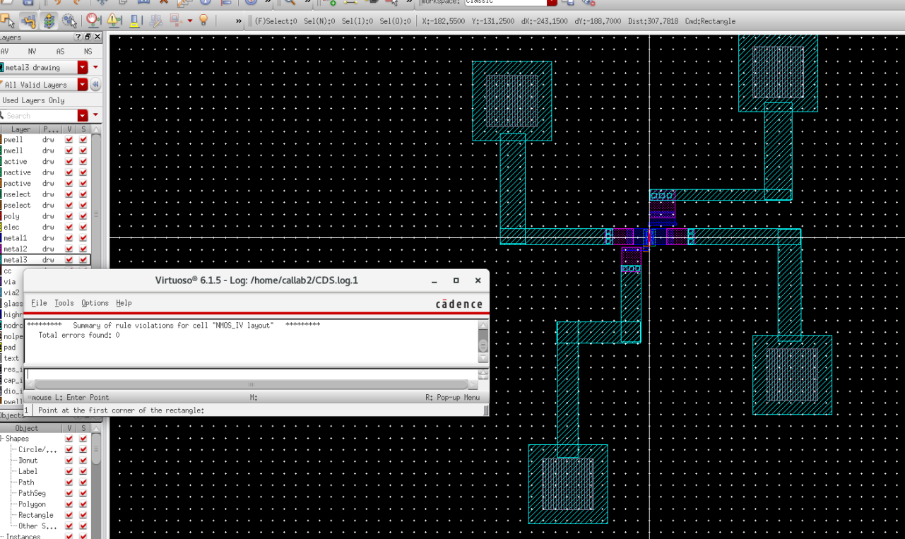
Next, we created a layout for out design and DRC our layout:

Then, we extracted our design and and did an LVS:

We then tested out extracted NMOS device:


We completed a similar process for the PMOS:


Lab:
ID v. VDS of an NMOS device for VGS varying from 0 to 5 V in 1 V steps while VDS varies from 0 to 5 V in 1 mV steps:


ID v. VGS of an NMOS device for VDS = 100 mV where VGS varies from 0 to 2 V in 1 mV steps:


ID v. VSD (note VSD not VDS) of a PMOS device for VSG (not VGS) varying from 0 to 5 V in 1 V steps while VSD varies from 0 to 5 V in 1 mV steps:


ID v. VSG of a PMOS device for VSD = 100 mV where VSG varies from 0 to 2 V in 1 mV steps:


NMOS Layout:


PMOS Layout:


Return...