Lab 2 - EE 421L
Author: Edgar Amalyan
Email: amalyane@unlv.nevada.edu
Date: 09/09/2020
Goals:
This lab focuses on the understanding of a 10-bit ADC and DAC circuit.
Additionally, we will implement our own DAC.
Prelab
Setup
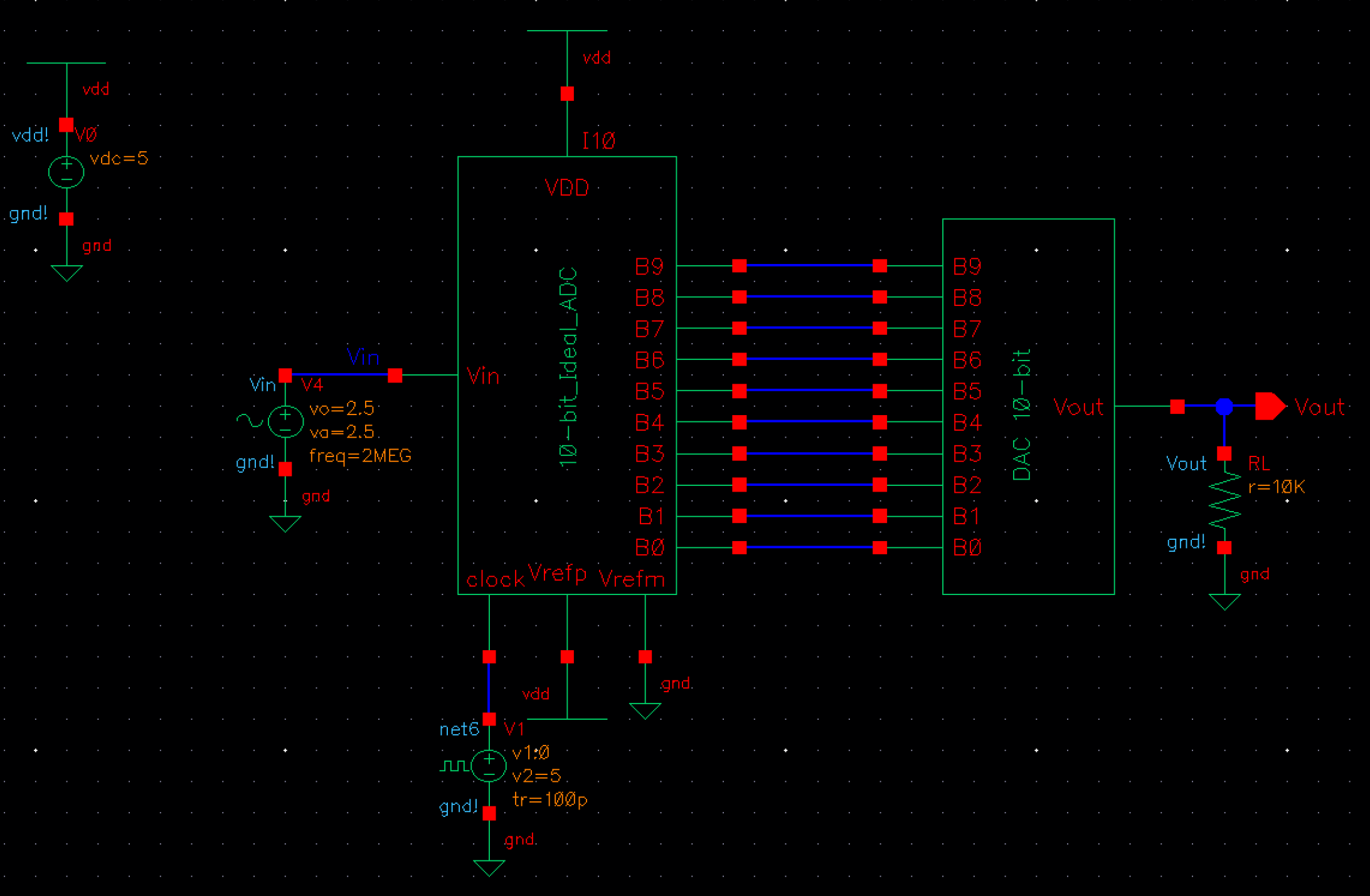
Provided
for us are certain Cadence schematics and simulations for the circuits and
components used in this lab. After importing these files into our
library, we open the sim_Ideal_ADC_DAC schematic.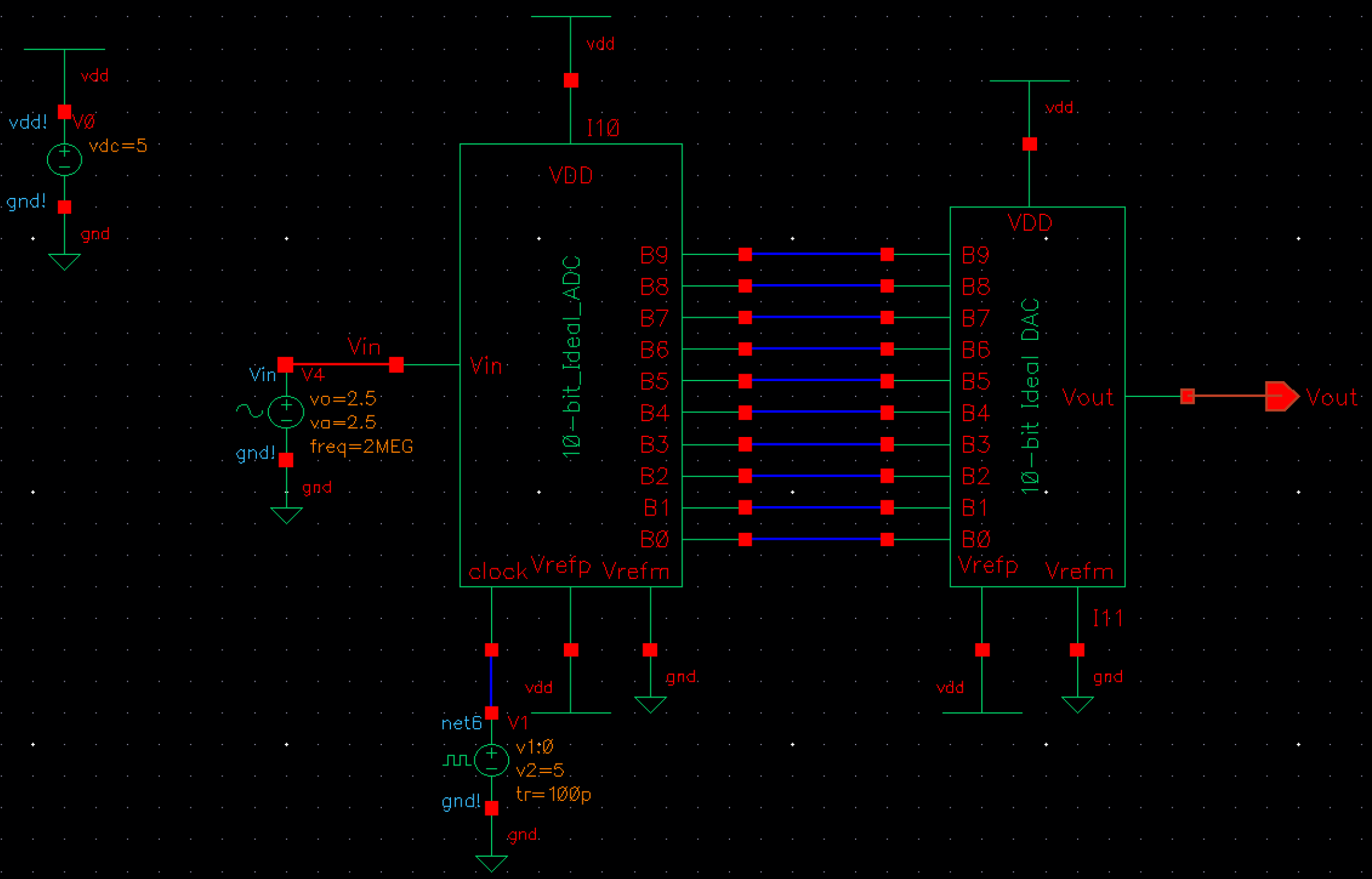
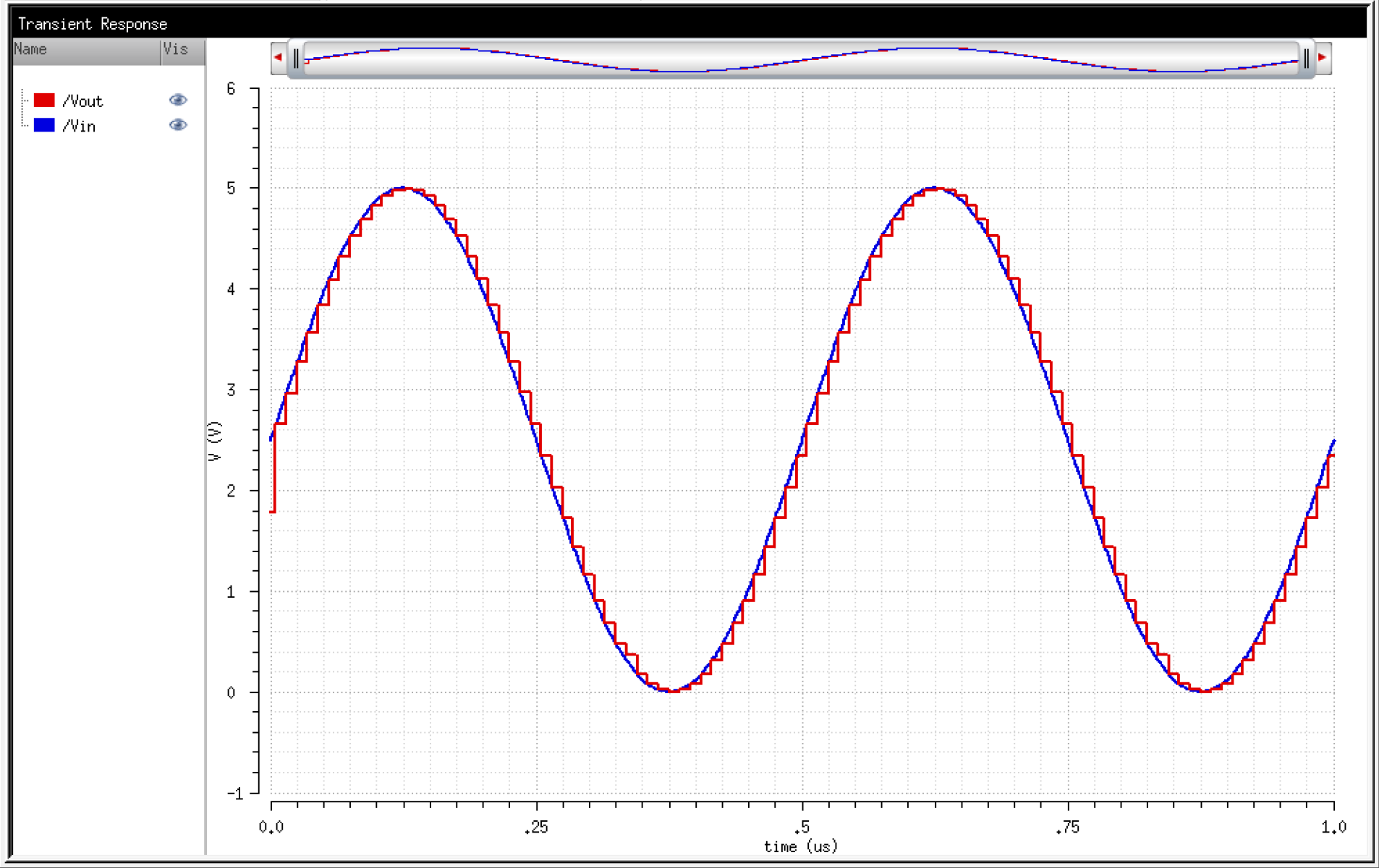
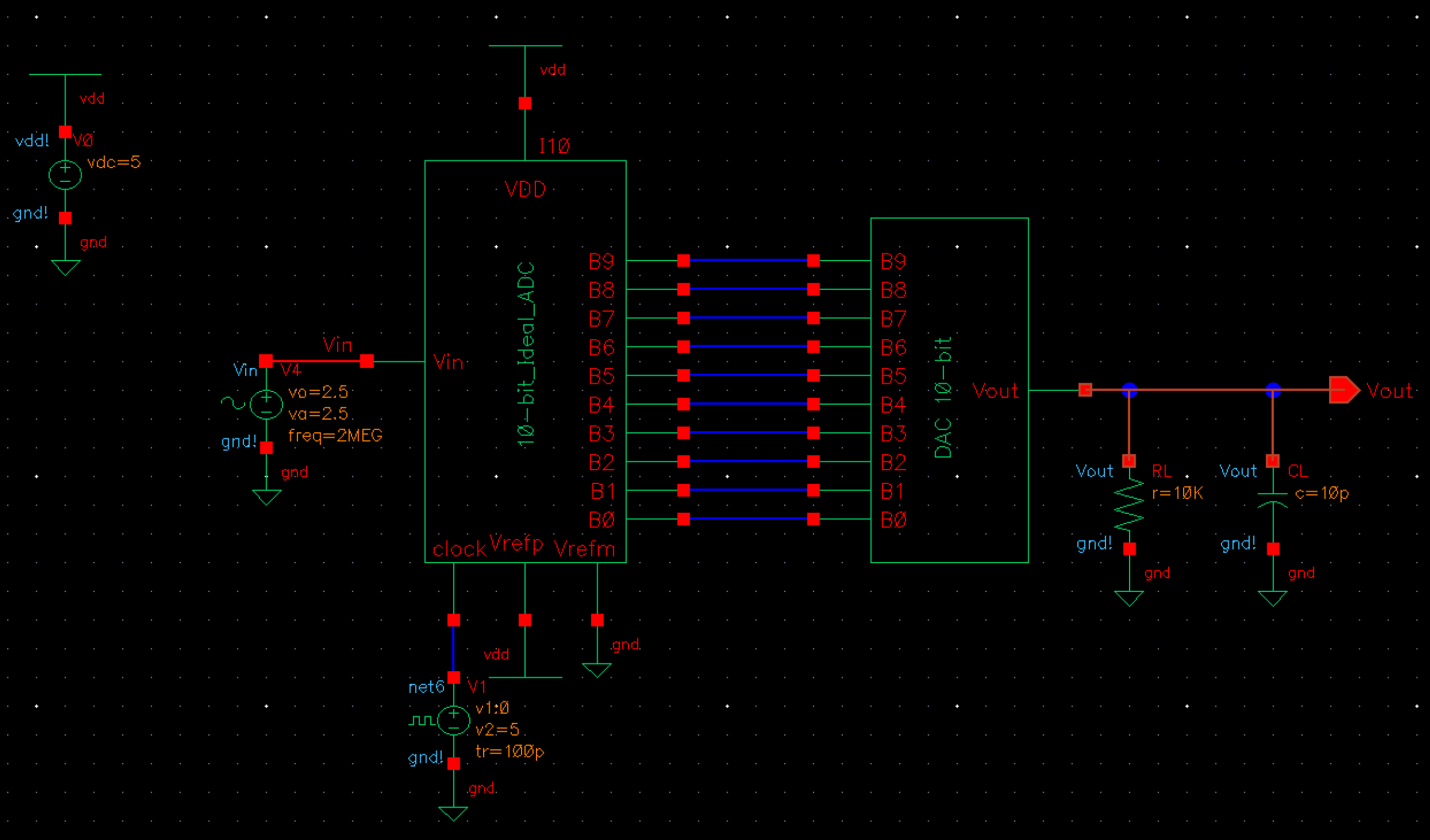
The
circuit takes in an analog input, Vin, into an ADC. The ADC outputs a
digital signal. The signal is fed into the DAC, which then converts it
back into an analog signal.
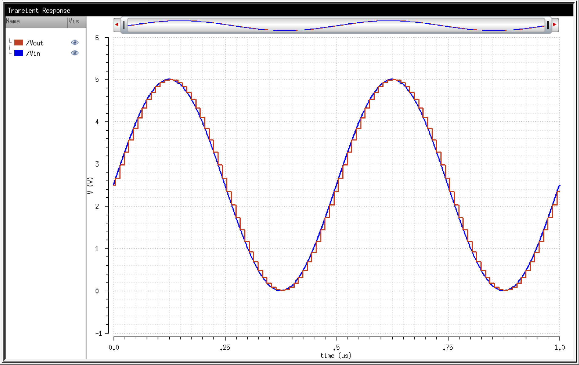
We expect Vout to be equal to Vin.
The simulation settings are provided to us, so we load them and run it.
Question: How is Vin related to B[9:0] and Vout?
B[9:0]
is a 10-bit bus representing the current value (in time) of Vin. The
bits are created by the ADC. B0 is the LSB and B9 is the MSB.
These
bits are then taken into the DAC and a resultant analog output is
generated. This analog output, Vout, is essentially the same (in both
magnitude and phase), as Vin.
The stair casing is a consequence of the limited bit depth of the DAC (as well as bit depth and sample rate of the ADC).
Determining the LSB
The
LSB is equal to VDD / 2^N, where N is the resolution of the DAC. In
our circuit, VDD is 5V. Since we are using a 10-bit DAC, our LSB = [5V / 2^10] = [5V / 1024] =~ 4.88mV.
Note
that a smaller VDD would be more
appropriate for small signals, and a larger VDD would be more
appropriate for larger signals. As VDD becomes
smaller, the range in which you can measure decreases, but the
precision increases. As VDD becomes larger, the precision decreases,
but the range increases. Since our circuit is essentially ideal, all
the parameters can be adjusted
to perfectly fit the situation. Of course practically, there are drawbacks and limitations.
One way of demonstrating the LSB in simulation is to use an input signal amplitude less than the LSB.
For
example, we can set the amplitude to 2mV. The DC offset is set to
2.44mV. The main point of the DC offset is to fit the AC waveform in
the appropriate range. Since VDD is 5V, any value of AC above 5V will
be clipped. On the other hand, since our circuit does not implement
two's complement, negative numbers cannot be represented, so the AC
should not fall below 0.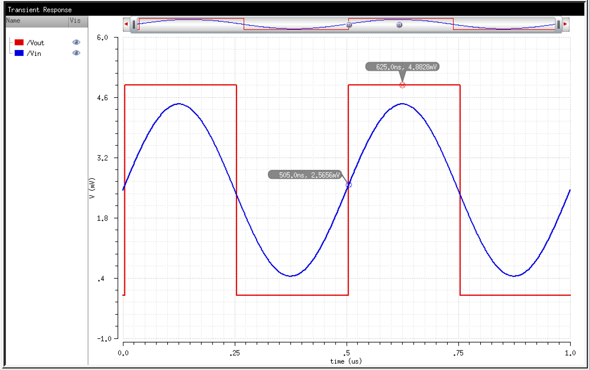
As seen, when the input reaches 2.56mV,
the output jumps to 4.88mV. The minimum voltage that can be reported by
the DAC (and ADC) is 4.88mV. Note that the trigger
point is a function of many variables, including the input amplitude,
offset, frequency, and sampling rate. In this example, an output is
generated around half of the LSB, but this will not be the case if the
listed values are changed.
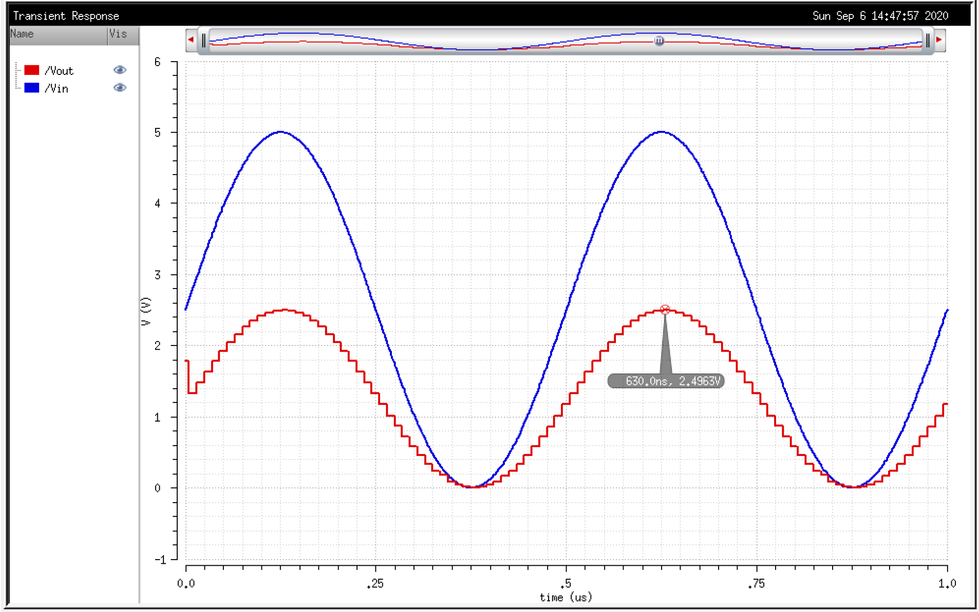
Understanding of the ADC & DAC
The other important parameter with regards to ADCs and DACs is the sampling rate. In
our circuit, the DAC has an infinite sample rate, as it just passes the
input to the output using a voltage divider. The ADC however has a
clock. In our circuit, the clock is set to a period of 10ns, so 200MHz.
Since our input signal is 2MHz, we sample at a frequency 100x the
maximum input frequency. This is enough to accurately reconstruct the
sine wave.
Let's
now change the input frequency to 50MHz. This is exactly half of our
sample rate, otherwise known as the nyquist frequency.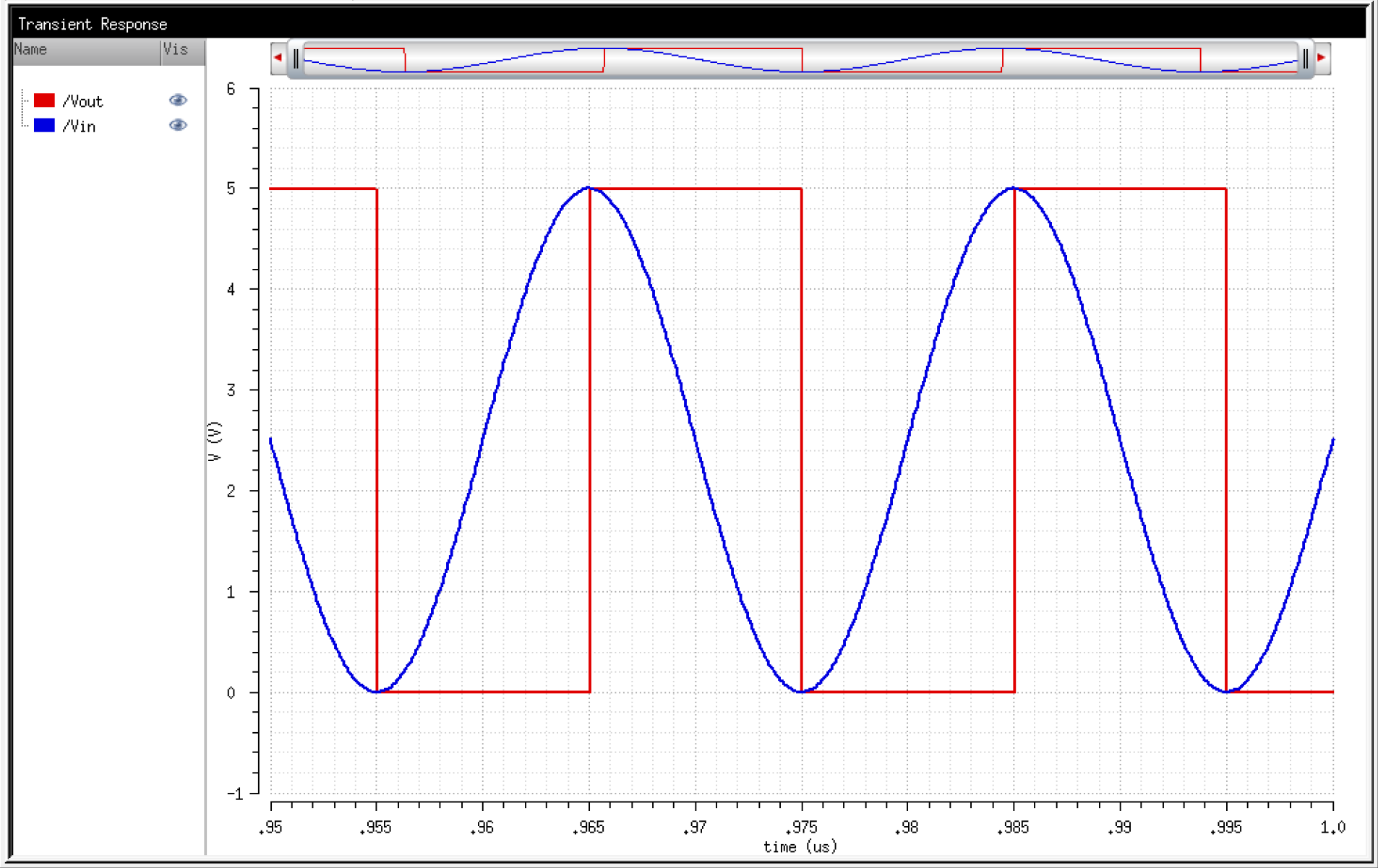
As
can be seen, at the nyquist frequency, the frequency and amplitude of
the original signal can be reconstructed. Note that 2x the sample rate
is not enough to create an identical replica, as the input is a sine wave, and the output is a square wave!
Lab
Design - Schematics, Symbols, Simulations
Here we will design our own 10-bit DAC based on the voltage-mode model presented in the book.
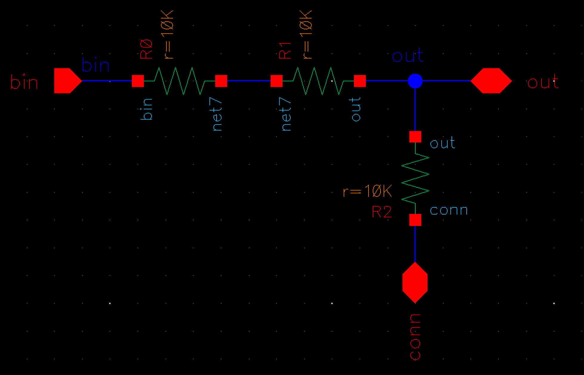
We
start by creating a 1-bit DAC. This is essentially a 1/3 voltage
divider. Since we are only running simulations, generic 10k resistors
can be used. In Lab 3, we will use custom 10k n-well resistors created
for the ON 0.5um process.
The connections are:
bin - the binary output from the ADC
out - the output of the 1-bit DAC
conn - used to connect to the next 1-bit DAC.
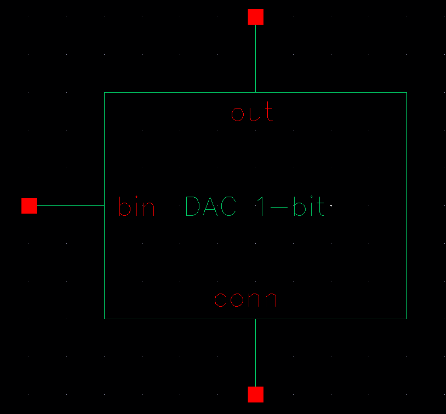
Since we are going to use ten of these 1-bit DACs, we should create a symbol to allow for a cleaner schematic.
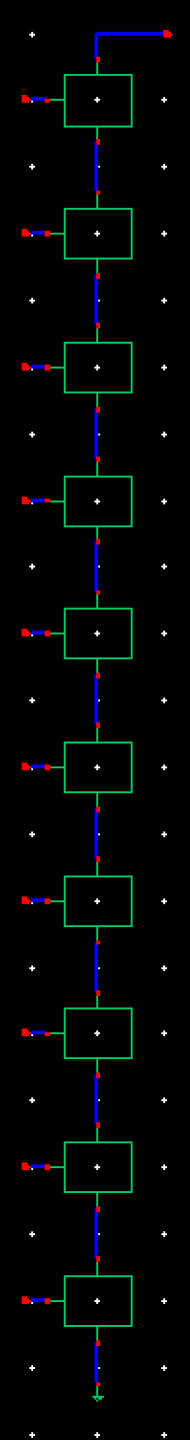
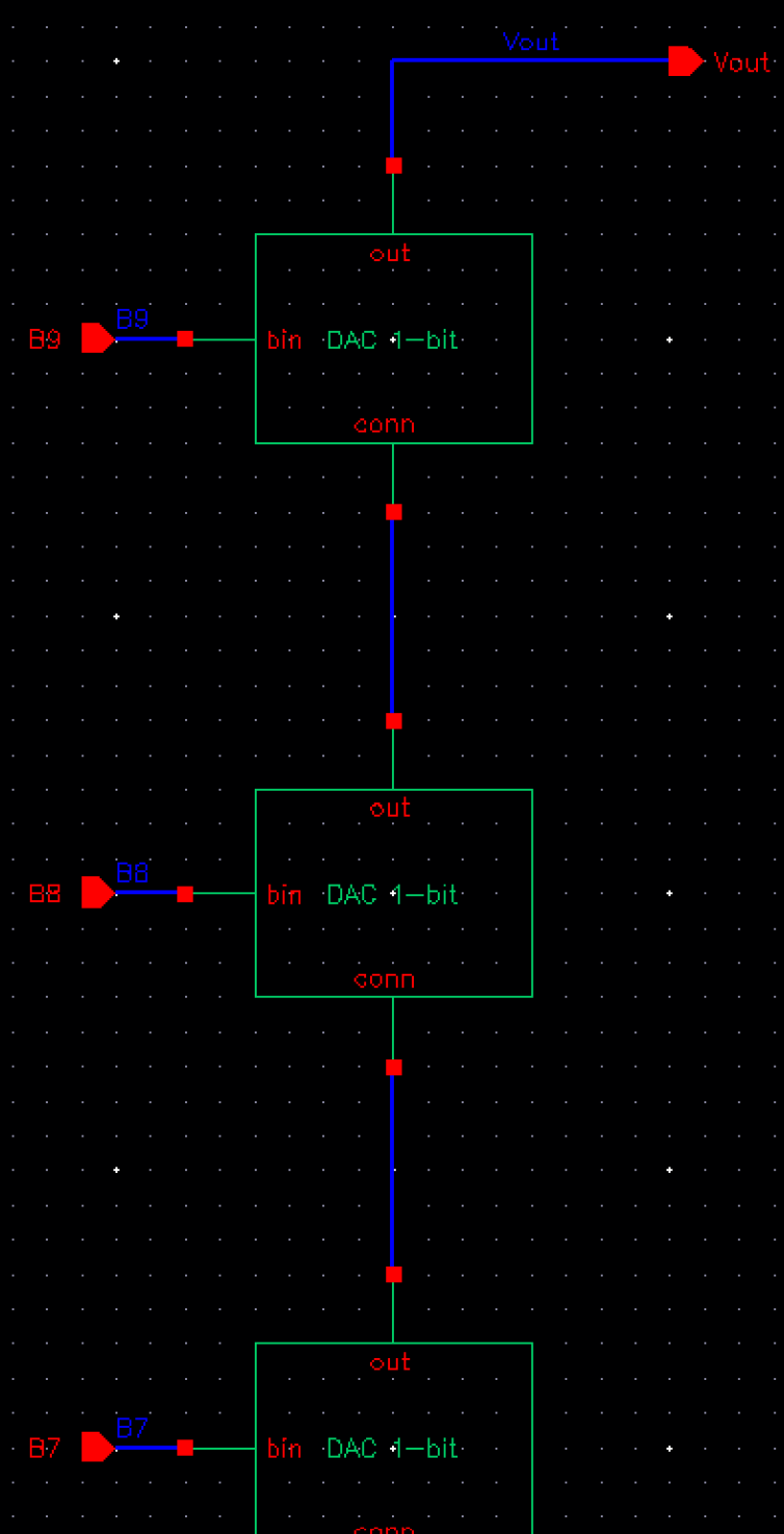
Next, we instantiate ten 1-bit DACs to create a 10-bit DAC. A close up can be seen to the right.
Since we will be using the 10-bit DAC in another circuit, we should make one more symbol for a more concice schematic.
Note
that this hierarchical structure is very useful for complicated
designs, designs with many components (the same or different), and
overall layered schematics in where one or more circuits are the
building blocks of another.
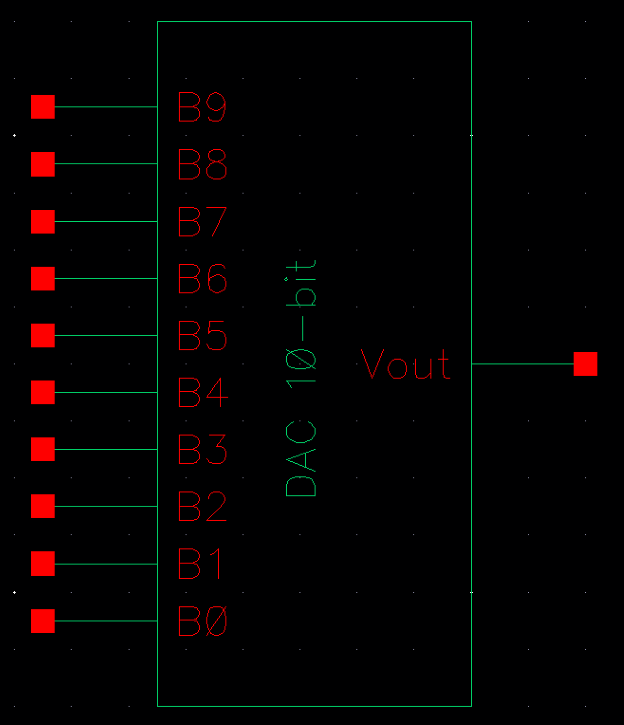
As for the symbol itself, we make sure it matches the footprint of the DAC provided to us.
We can now replace the existing DAC in the provided schematic with our new DAC and simulate.
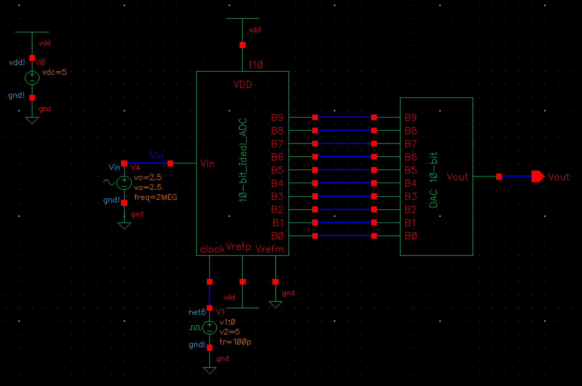
Note
here that some simulation parameters can result in early terminations
or convergence problems. To fix this, we can change the max step in the
transient options and set the relative tolerence in the AC simulation
options to 1e-2.
This will allow for the simulation to complete, remove convergence problems, and eliminate trapezoidal ringing in the
output waveform.
Determining DAC Output Resistance
The
output resistance of the DAC can be calculated using an equivalent
thevenin circuit. We have 2 equivalent resistors in series in parallel
with another equivalent resistor. This yields a total resistance of R.
Since the DAC is built using these 1-bit circuits, this thevinizing procedure can be repeated until the final output
resistance, R, or in our case, 10k, is reached.
Driving a Capacitive Load and Delay
If
the DAC is driving a load with a capacitance of 10pF, the delay can be
calculated using 0.7RC. Since we just calculated R to be 10k, we see
that the delay is equal to 0.7 * 10k * 10pF = 70ns.
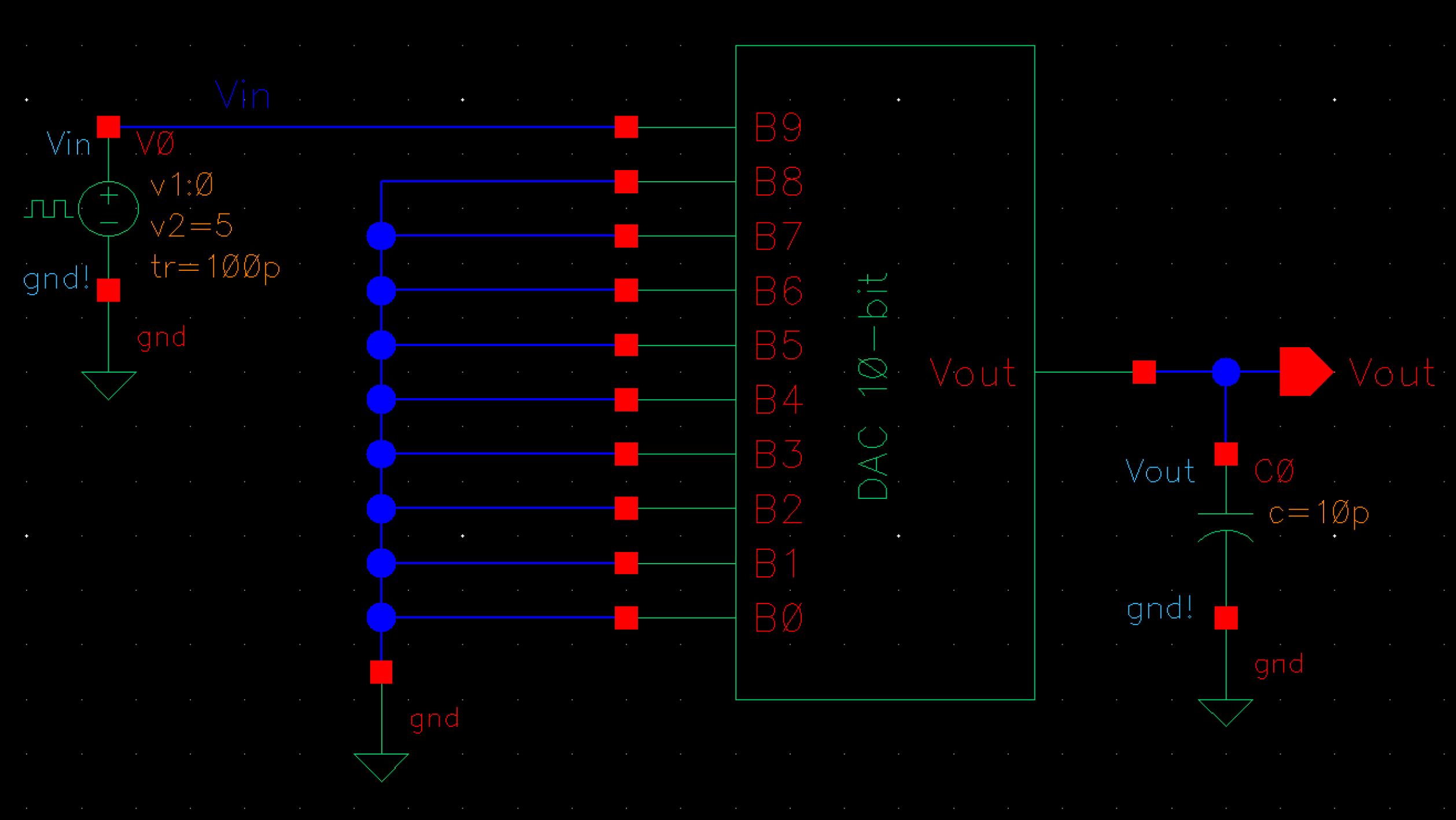
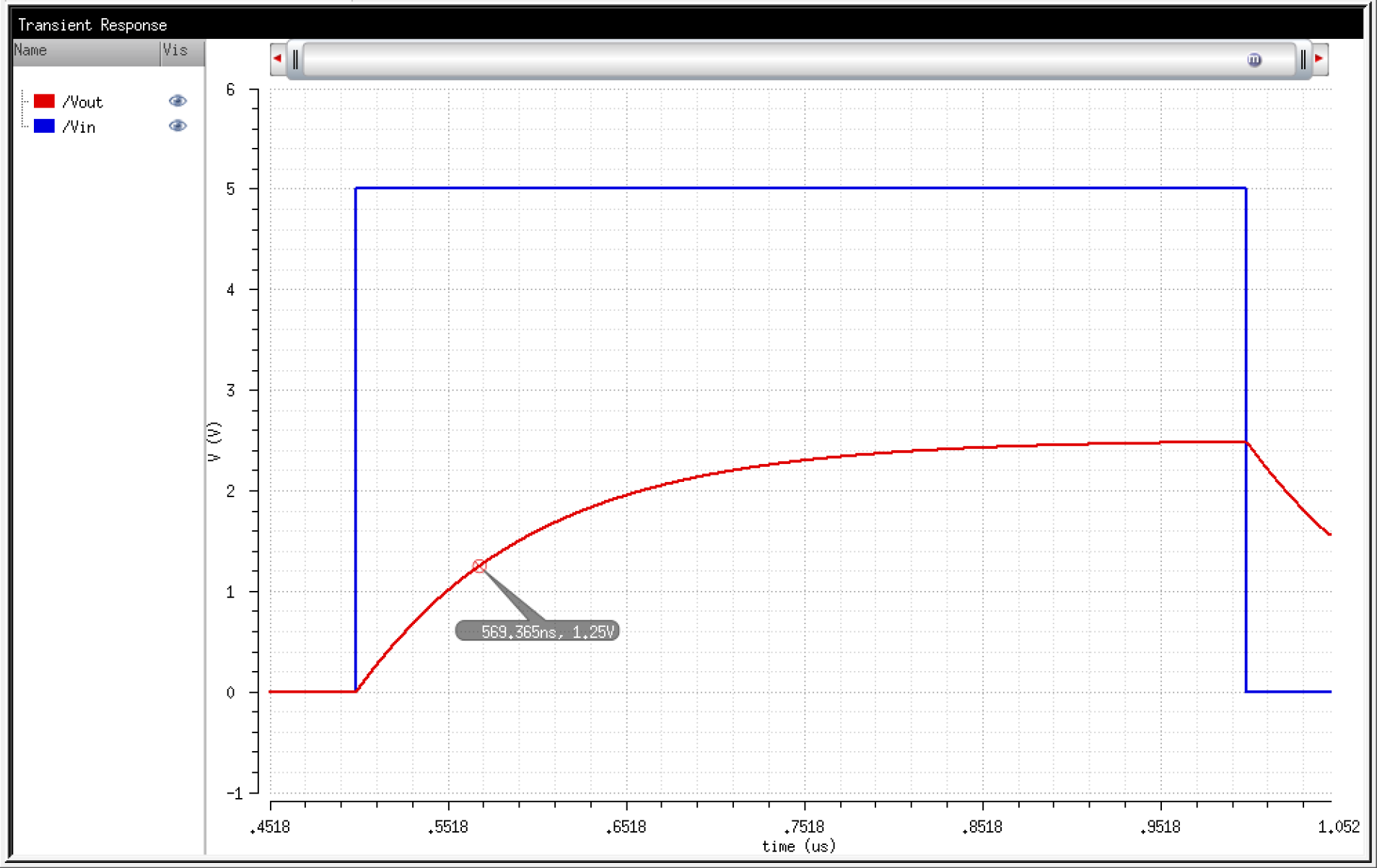
Here
we can see that the time it takes to reach 1/2 of the input pulse, or
the maximum voltage on the capacitor, is 569.365ns - 500ns =~ 70ns.
Simulations of Functionality
Back to the ADC and DAC circuit. We will simulate the circuit with a resistor, a capacitor, and then with both.
R:
We can see what happens when the DAC drives a 10k resistive load.
As expected, the voltage is halved, as a 10k load in series with the 10k output resistance creates a 1/2 voltage divider.
C:
Next we can see what happens when the DAC drives a 10pF capacitive load.
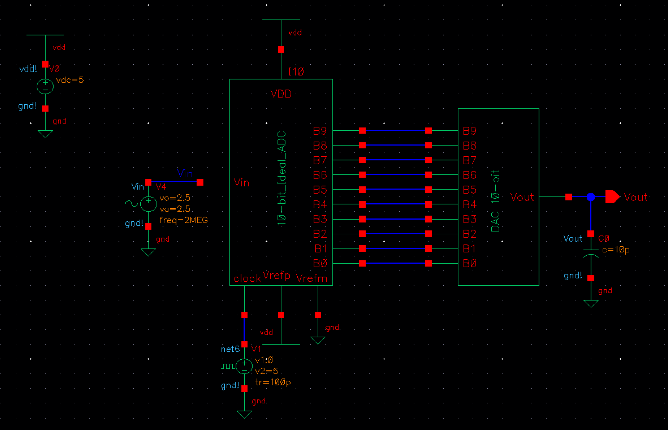
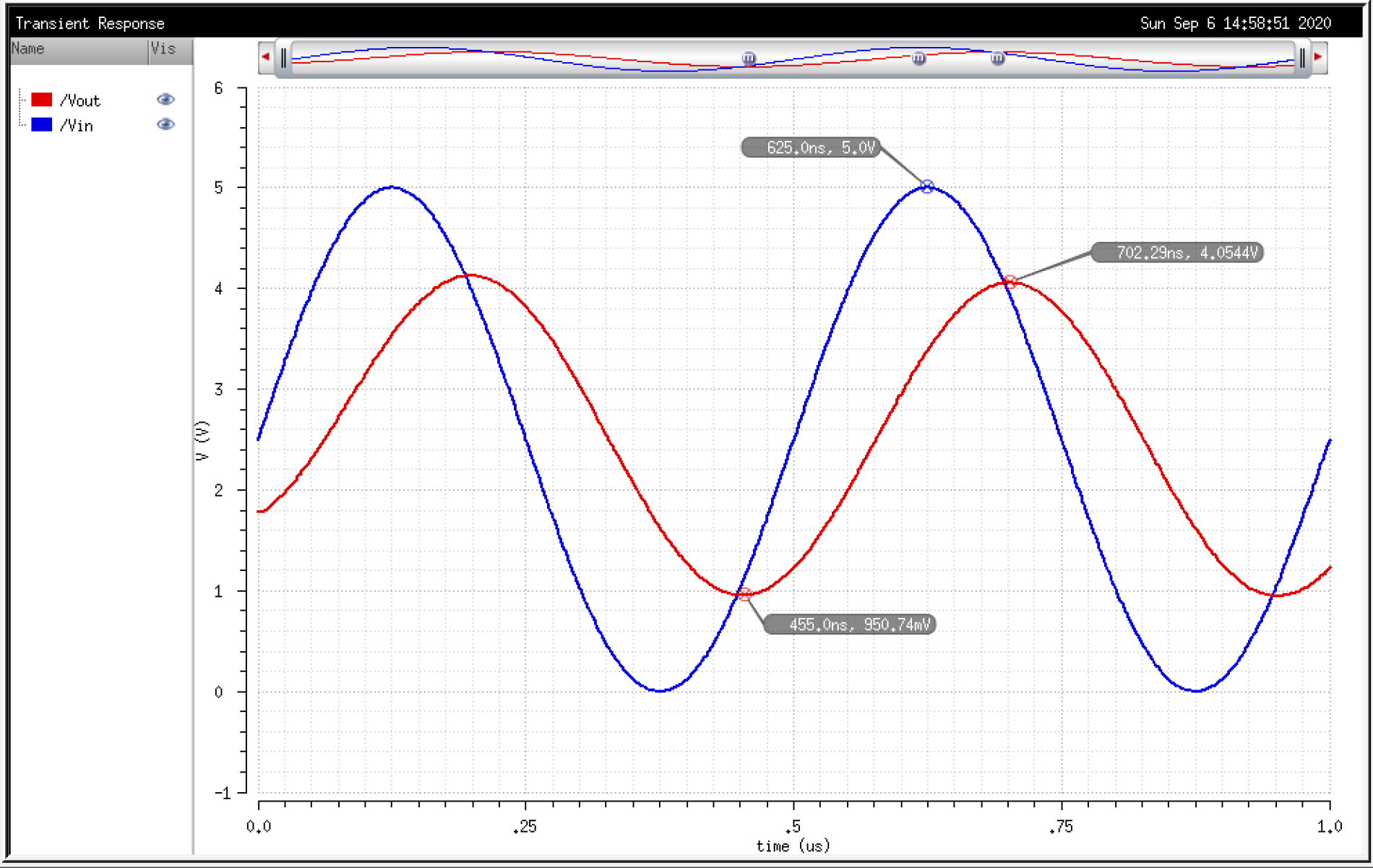
The
output is slightly smoother (not as many jagged edges). Vout lags Vin
by around 75ns due to the RC time constant. The Vpp of the output is
about 3.1V. So 3.1 / 2 = 1.55 + 0.950 =~ 2.45 positive DC bias.
RC:
Finally, we can simulate with both the resistor and the capacitor.
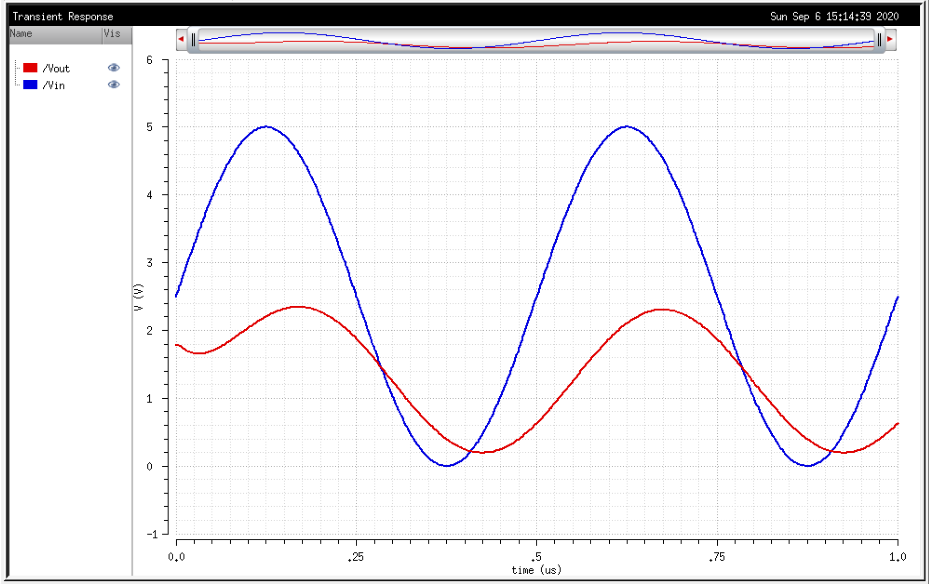
The
effects of both the resistor and capacitor come into play now. To
calculate the result (assuming steady state), we can find the equivalent impedence of the
resistor and capacitor and perform a voltage divider with the 10k
output resistance of the DAC.
The
resulting voltage is about half the input with a delay, albeit smaller
than the one with just the capacitor, as the resistor in parallel
lowers the impedance.
Question/Discussion:
What happens if the resistance of the switches isn't small compared to
R, for example in a real circuit in which the ADC outputs are MOSFETs?
The
outputs of the ADC in our circuit are zero resistance wires. If these were implemented
using transistors, then the output impedence of the DAC would change.
Recalculations would be necessary to match the output with connected
loads.
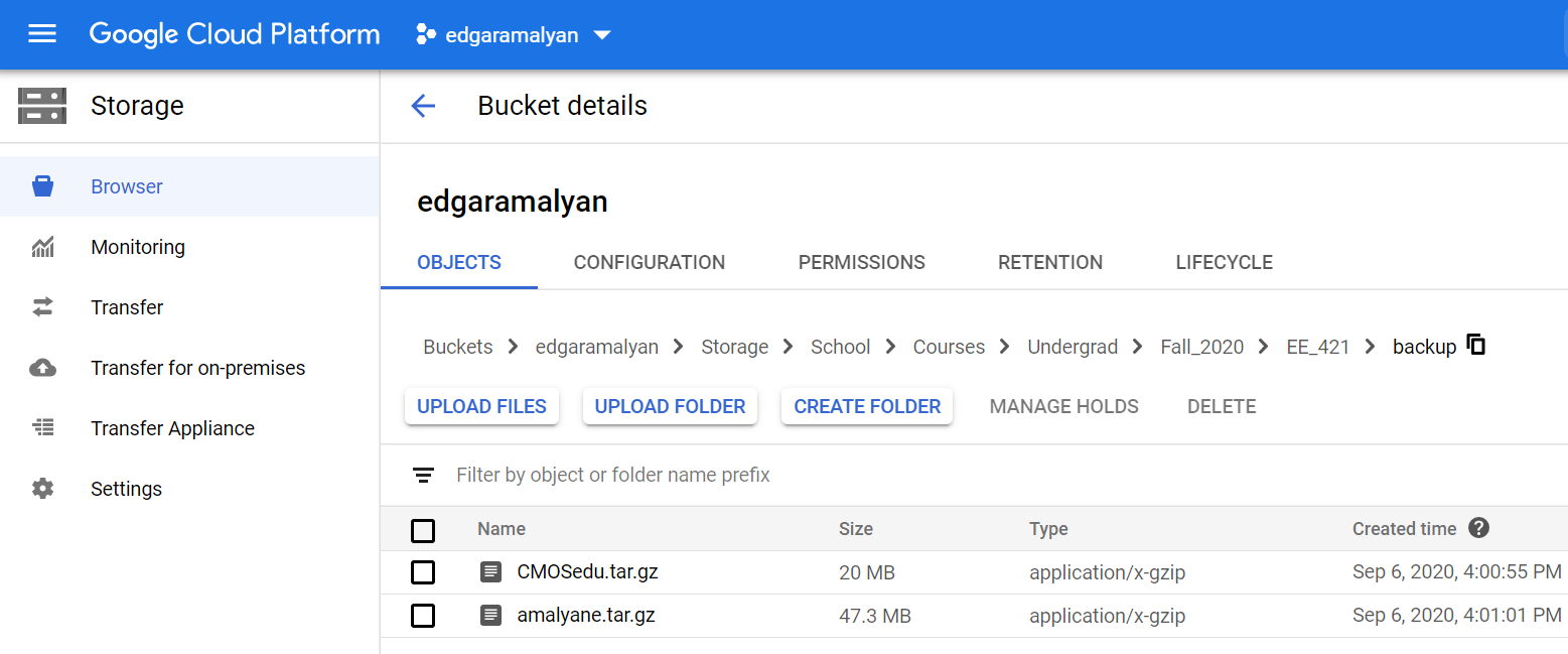
Backups:
As
demonstrated in Lab 1, I run ./backup.sh from the Cadence server and
download the 'Backup' folder containing the compressed archives of my
CMOSedu and entire home directories.
All files pertaining to this lab report already exist and are directly edited from another folder that also gets synced.
I run sync_to_gcp.bat from my computer which makes my GCP Storage bucket identical to my local directory.
Return to EE 421L Labs