Final Project - EE 421L
Email: alvara6@unlv.nevada.edu
November 18,
2020
Lab Project Description
Tasks
·
Project (not a group effort,
each student will turn in their own project) – design, layout, and simulate a
digital receiver circuit that accepts a
high-speed digital input signal D and Di (a
differential pair connected to your circuit from, for example, a twisted pair
of wires such as in an
Ethernet cable). D and
Di are complements so, for example, if D is 5V then Di is 0V and output = 1.
Another example, when D is 1V and Di is 2V
then output = 0. At
high-speeds and long distances the voltages received aren't full digital logic
levels (i.e., 5V and 0V), hence the need to design,
and use, a
high-speed digital receiver circuit. Ideally, when D > Di the
receiver outputs a 1. When D < Di the receiver outputs a 0.
Base your
design on
the topology seen in Fig. 18.23. Try to design for high-speed and
low-power. Characterize your design (in sims) and the trade-offs.
For example, show that
you get higher-speed if you use more energy (burn more power). See if you can
get, in this 500 nm process, 250 Mbits/s
(a bit width of 4 ns)
with an input voltage difference of, for example, 250 mV (with D and Di
swinging back and forth between 2.75V and 3V,
for one of many
examples, your circuit outputs the correspondingly correct values). Note that
while Fig. 18.23 shows one inverter on the output
you may find, for
example, that two inverters work better (at the cost of power). Use a
table to summarize your design's performance.
Schematic(s)

Figure 1 –
N-TYPE Self Biasing Diff Amp

Figure 2 –
P-TYPE Self Biasing Diff Amp

Figure 3 –
Final Schematic used in which P and N-TYPE Self Biasing Diff Amp are connected
in parallel.
I decided to
have two inverters in my design to give a cleaner and more precise output
waveform. In exchange for
Better outputs
it uses more power.

Figure 4 – A
symbol was made for the final schematic and this is the circuit that I have
used to test for different parameters.
In this figure
you will see the symbol made, 2 voltage pulses (two voltages swinging back and
forth i.e. = 2.75V – 3V), and a VDD.
Results Table
|
Testing at Different Widths for PMOS and NMOS (Lengths left
@ 600n) |
|
|
1. PMOS =
12u, NMOS = 6u Time Delay = 756ps |
|
|
2. PMOS = 6u, NMOS = 3u Time Delay = 769ps |
|
|
3. PMOS = 3u, NMOS = 1.5u Time Delay = 841ps |
|
|
Conclusion about this Test: Since this project was done using the 500nm process I decided to keep
the lengths of 600n (minimal length in the 500nm). To test for different
delays I changed the top PMOS and the bottom NMOS of the schematic because
these are the components of the ciircuit that control the circuit. I decided
to test three different widths for the PMOS/NMOS that are: 12u/6u, 6u/3u,
3u/1.5u. What I concluded is that the smaller the values were than the higher
the delay got. When wanting to get a faster delay we should be increasing the
widths and decreasing the lengths. The sims verify this theory. I ended up
choosing the 12u/6u widths for the PMOS/NMOS because I wanted my design to
work very fast. |
|
|
|
|
|
Testing at Different Frequencies |
|
|
4. Bit Width = 4 ns Rise Time Delay = 761ps |
|
|
5. Bit Width = 4 ns Fall Time Delay = 739ps |
|
|
6. Bit Width = 2ns Rise Time Delay = 752ps |
|
|
7. Bit Width = 2ns Fall Time Delay = 747ps |
|
|
8. Bit Width = 1ns Rise Time Delay = 746ps |
|
|
9. Bit Width = 1ns Fall Time Delay = 735ps |
|
|
Conclusion about this Test: I ran the 12u/6u PMOS/NMOS schematic at different bit widths which were
4ns (1 / 4ns = 250 Mbits/s), 2ns (1 / 2ns = 500 Mbits/s), 1ns (1 / 1ns = 1
Gbits/s). What I noticed about running this test is that my cicuit reacted
very well to running fast frequencies. For all three frequencies the rise and
fall delay times were around 700ps. In my opinion this is very well, because
all of these delay times were faster than 1ns. One side note about this test
is that when freqeuncy is increased the bit widths start to get more rounded.
|
|
|
|
|
|
Testing Power at Different Frequencies |
|
|
10. P_AVG = 9.005mW Bit Width = 4 ns |
|
|
11. P_AVG = 9.532mW Bit Width = 2 ns |
|
|
12. P_AVG = 10.18mW Bit Width = 1 ns |
|
|
Conclusion about this Test: After running this test I saw that faster frequency, also means that
more power is being used up. This is one of the tradeoffs of my design, is that although this circuit works very
well for fast frequencies (as demonstrated above), it also uses more power. The equation that was used to figure
out average power: P_AVG = VDD *
I(AVG) = C(Tot) * VDD ^2 * f(clk). There are two ways on Cadence to solve
for average power. The first is to plot the I(VDD) and then in the calculator
use the function average and multiply by VDD. The second way is to go to
results in the ADE (analog design environment) window and open the “psf” file
and click and plot the pwr. Later then just avergage this number by using the
average function in the calculator. I chose the latter, but both give the
same results! |
|
|
|
|
|
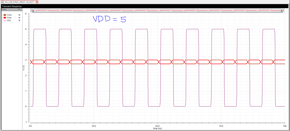
Testing at different VDDs |
|
|
13. VDD = 5V |
|
|
14. VDD = 4V |
|
|
15. VDD = 3V |
|
|
16. VDD = 2V |
|
|
Conclusion about this Test: I ran simulations where I changed VDD from 5V to 2V. At VDD = 5V the circuit
is working fine and this will be the control of this test. As I changed the
VDD to 4V we can see that the output wavefrom is reduced by one volt so
instead of 0-5V, it now outputs 0-4V. For the next simulation VDD is changed
to 3V and the simulation shows that the ouput is not correct now starting
from 2.95V to ending up at 3V. The final sumlation run is when VDD = 2V, as
the simulation shows this VDD does not work and now the output voltage does
not switch at the VSP (switching points), but instead it is a constant 2V. We
can conclude for this schematic that the best VDD voltage is 5. For VDD = 4V
it does not output full logic level, and for VDD 3 and 2 the output is wrong. |
|
|
|
|
|
Testing of different temperatures using parametric anaylsis |
|
|
17. 0° to 100°Celsius |
|
|
Conclusion about this Test: After runnning this circuit from 0° to 100°Celsius we can see that
the delay increases when the temperature increases. The images above show the
menu for the parametric analysis where we choose the variable “temp” and run
this linearly from 0 to 100 Celsius. To show this waveform I zoomed in on the
window to show how the temperature effects this circuit. |
|
|
|
|
|
Testing of different Vinm and Vinp |
|
|
18. Vin(1)
= 3V Vin(2)
= 2.75V |
|
|
19. Vin(1)
= 3V Vin(2)
= 2.8V |
|
|
20. Vin(1)
= 3V Vin(2)
= 2.85V |
|
|
21. Vin(1)
= 3V Vin(2)
= 2.9V |
|
|
22. Vin(1)
= 3V Vin(2)
= 2.95V |
|
|
23. Vin(1)
= 3V Vin(2)
= 2.96V |
|
|
24. Vin(1)
= 3V Vin(2)
= 2.97V |
|
|
25. Vin(1)
= 3V Vin(2)
= 2.98V |
|
|
26. Vin(1)
= 3V Vin(2)
= 2.99V |
|
|
Conclusion about this Test: The final test that I ran was having different voltage differnces
between Vinm and Vinp. My conclusion is that the circuit works fine when the difference
between voltages is greater than .10 V because the delays are under 1 ns and
the output are still full logic levels. A voltage difference smaller than .10
V has to large of a delay which is greater than 1ns.The volatge differences
of .02V and .01V do not output full logic levels. This is great that this circuit works so well, it is because we
are using buffers in parallel which complementary nature results in a buffer
that is robust and works over a wide range of operating voltages. |
|


Layout(s)
For the layouts I broke up
the final circuit into two parts to make it easier for me. The first part was
the N-TYPE circuit with 2 inverters attached,
The second part was the
P-TYPE circuit. I LVS’d
and DRC’d the layouts for the new schematics to make
sure they worked and matched. This ultimately saved me a lot of time
because for the final
layout I just had to add two metal 3 wires.
N-TYPE Schematic, Layout, and LVS + DRC

Figure 5 –
Schematic for the N-TYPE self-biasing diff amp connected to 2 inverters.

Figure 6 –
Layout of the N-TYPE self-biasing diff amp

Figure 7 – LVS
verification

Figure 8 – DRC
verification
P-Type Schematic, Layout, and LVS + DRC

Figure 9 -
Schematic for the P-TYPE self-biasing diff amp

Figure 10 –
Layout of the P-TYPE self-biasing diff amp

Figure 11 -
LVS verification

Figure 12 -
DRC verification
Final Schematic, Layout, and LVS + DRC

Figure 13 -
Schematic for the cascaded self-biasing diff amp

Figure 14 –
Layout of the cascaded self-biasing diff amp

Figure 15 -
LVS verification

Figure 16 -
DRC verification
Backing Up Work
As seen by the snips above these were the steps that I used to
back up my work. First, I found the folder in my CMOSedu folder
in the MobaXTerm.
After finding where the folder was, I downloaded the folder to the
desktop and later sent it to a compressed zipped folder.
After making a ZIP file I uploaded them to my google drive with
the date in the title. This should complete my backup process.
This concludes the Final Project of the High
Speed Digital Receiver.