Lab 7: EE 421L
Using buses and arrays in the design
of word inverters, muxes, and high-speed adders
Authored by: Kaylee Spencer
Email: spenck3@unlv.nevada.edu
Due: 11/06/2019
Lab Description: This lab is meant to teach us how to design, layout, and simulate word inverters, muxes, and high-speed adders using buses and arrays.
Prelab
Part 1
For the prelab, we needed to go through Tutorial 5. Below I have added a few images from the tutorial.

(ring oscillator schematic)

(ring oscillator layout)

(ring oscillator extracted layout)

(ring oscillator simulation schematic)
Lab
Part 1
First, we began by creating a more concise 4-bit inverter symbol by using an arrayed name (I0<3:0>). We then connect buses (wide-wire) to the input and output of the concise 4-bit inverter schematic (inv4), then create a new symbol.

(4-bit inverter symbol)

(concise 4-bit inverter symbol)

(CMOS inverter schematic)
Part 2
We then created a simulation schematic for the 4-bit inverter, naming it sim_inv4. As you can see below, all four of the inverters’ inputs are tied together to an input pulse source. The out<0> is not connected to a load while out<3> is connected to a 100fF load. The out<1> is connected to a 1 pF load while out<2> is connected to a 500 fF load.

(4-bit inverter simulation schematic)
Below you can see the graph of the outputs, as well as the input, of the 4-bit inverter simulation. Notice that the delay of the RC rise and fall times increase as the capacitive load increases at the output. However, we want our outputs to have sharp edges on the rise and fall.

(4-bit inverter simulation output graph)
Part 3
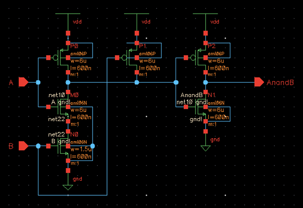
Next, we needed to create schematics and symbols for an 8-bit input/output array of a NAND gate, AND gate, NOR gate, OR gate and inverter.

(8-bit input/output NAND symbol)

(8-bit input/output schematic)

(CMOS NAND schematic)

(8-bit input/output AND symbol)

(8-bit input/output AND schematic)

(CMOS AND schematic)

(8-bit input/output NOR symbol)

(8-bit input/output NOR schematic)

(CMOS NOR schematic)

(8-bit input/output OR symbol)

(8-bit input/output OR schematic)

(CMOS OR schematic)

(8-bit input/output inverter symbol)

(8-bit input/output inverter schematic)

(CMOS inverter schematic)
Below I added the 8-bit simulation schematics for the NAND gate, AND gate, NOR gate, OR gate and inverter.

(8-bit NAND simulation schematic)

(8-bit NAND simulation output graph)

(8-bit AND simulation schematic)

(8-bit AND simulation output graph)

(8-bit NOR simulation schematic)

(8-bit NOR simulation output graph)

(8-bit OR simulation schematic)

(8-bit OR simulation output graph)

(8-bit inverter simulation schematic)

(8-bit inverter simulation output graph)
Part 4
We then needed to examine the schematic of a 2-to-1 DEMUX/MUX (de-multiplexing and multiplexing). We created our own 2-to-1 DEMUX/MUX schematic and symbol.

(DEMUX/MUX schematic)

(DEMUX/MUX symbol)

(MUX simulation schematic)

(MUX simulation output graph)

(DEMUX simulation schematic)

(DEMUX simulation output graph)
Part 5
Next we needed to create an 8-bit wide word 2-to-1 DEMUX/MUX schematic and symbol. It was required to include and inverter in our design so the cell only needs one select input, S.

(DEMUX/MUX with inverter schematic)

(8-bit DEMUX/MUX with inverter symbol)

(8-bit DEMUX/MUX schematic)

(8-bit DEMUX/MUX symbol)

(8-bit MUX operation simulation schematic)

(8-bit MUX operation simulation output graph)

(8-bit DEMUX operation simulation schematic)

(8-bit DEMUX operation simulation output graph)
Part 6
We needed to draft the schematic of the full-adder seen in Fig. 12.20 using 6u/0.6u devices, both NMOS and PMOS. We first created a single full-adder schematic, symbol and layout, which we had previously done in Lab 6.

(single full-adder schematic)

(single full-adder symbol)

(single full-adder layout)

(single full-adder extracted layout)
Next, we drafted a schematic, symbol, layout and extracted layout for an 8-bit full-adder, showing that they DRC and LVS.

(8-bit full-adder schematic)

(8-bit full-adder symbol)
![]()

(8-bit full-adder layout)

(8-bit full-adder extracted layout)
Finally, we created an 8-bit full-adder operation simulation schematic and displayed the output graph below.

(8-bit full-adder operation simulation schematic)

(8-bit full-adder operation simulation output graph)
Now that we have finished the lab, I backed up my work to my Google Drive.