Lab 8 – Generating a Test Chip Layout for Submission to MOSIS
EE 421L Digital IC Design
Lab Date: 11/27/19 Due: 12/04/19
By David
Santiago – Email: santid4@unlv.nevada.edu
// By Mohammed
Islam – Email: islamm1@unlv.nevada.edu
Last Edited on
12/04/19 at 3:26 using Word
David Santiago
-Provided Boost SPS
-Layout
-Lab Report
Bryan Kerstetter
-Provided Clock Multiplier
-Chip Layout
-Aided in Lab Report
Muhammed Islam
-Aided in layout of voltage divider
and ring oscillator. Joined another group.
In this lab,
we will be taking layouts and placing them on a 40-pin pad frame that will be
fabricated by MOSIS.
Prelab:
We will be
using the Tutorial Libraries created from CMOSedu.com.
Starting by
copying Tutorial 5 into a new library, Tutorial 6:

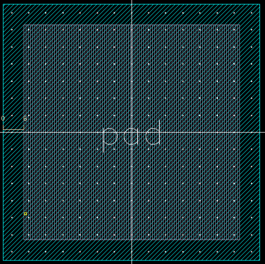
Creating a new
layout, “pad_75u”, with a metal3 75μm square, and glass 63μm square,
with 6μm distance of separation:


Creating an
input/output metal3 pin, “pad”, on top of the entire pad.
For the big 40 pin layout, we will have a max size of 1.5mm on any
side, and 10 squares per side (plus 2 for the corners).
Therfore, 1.5mm / 12 =
125μm cell size. So, let’s create a text layer (ignored in MOSIS ruleset),
of 125μm x 125μm:

Pad DRC:

Creating a new
layout cell, “padframe”, and instantiating the pad, and then applying an
input/output pin “pin<1>” on metal3:

Doing the
whole square:

We see the
textboxes really helped with setting the distances between the squares.
Go back to the
original single pad, and delete the textbox. Check and
save.
After that,
relabel every pin on the square to “pin<1>,pin<2>,
…pin<40>”


DRC of the
padframe:

Creating a pad schematic and padframe schematic (Use Check ->
Find Marker to ignore the floating pin):
Schematic for
a single pad:

Symbol for
single pad:

Schematic of
the padframe:

Symbol of the
padframe:

Creating a
schematic cell, “chip”:

Check and
Save:

There are
unused pins in the padframe. This is ok. We will ignore these warnings by
clicking Check -> Find Markers, and hit Ignore:

Alternative (if you have
problems with the DRC not accepting the ignore requests):
Instantiate a
cell, “noConn”, from the basic library:

In this part,
I will organize my noConn connections based on the
array sizes.
For the first
array (pin<2:3>), instantiate an array of noConn
connections, I#<2:3> (where “#” is a number) by pressing q and doing the
following:

Creating
busses and following this pattern:

Laying out everything
(Focusing on just getting everything to LVS):

Connections at
Ring Oscillator:

NAND:

Inverter:

PMOS:

NMOS:

R_div:

Ring
Oscillator:

Final Layout:

Grand DRC:

Grand Extracted:

Grand LVS:


--------------------------------------------------------
Lab Schematic:
For this lab,
we will place many components into a schematic, and then place the layouts into
a padframe.
Creating a
Cadence Library, “Chip1_f19”, with “Chip1_f19” as the main layout and schematic
cell.
After that,
looking at a cell that is instantiated in a different Library, and copying the highest hierarchy with the
following settings:

This will then
copy everything that was needed for the main hierarchy cell:

The other main
thing that will be useful is a buffer that is able to drive an off-chip
capacitance from a scope probe.
Here is the
buffer system:

With this
system, we have a 2-stage inverter which will “buff” the signal going through
the buffer all the way to a heavy 30pF Off-Chip Capacitive load.
The diodes at
the output will protect the output and let the current run into the diodes, and
not into the output.
David S’s Boost Switching Power
Supply:

Pins used:
|
Chip Pin # |
Pin
Description |
Comments |
|
32 |
VDD_DS |
Power
Supply DS |
|
33 |
Out_DS |
Boost
SPS DS (NMOS) |
|
34 |
Vout_DS |
Boost
SPS DS (Sense) |
|
35 |
gnd! |
Ground
|
|
36 |
gnd! |
Ground |
|
37 |
VDD_DS |
Power
Supply DS |
How to test:
1. Connect VDD_DS
together to a power supply. Ground can be common to other components in the
circuit.
2.
Pin<33> will be connected to an Inductor (65μH to 85μH) that is
connected to VDD_DS and the Anode of a Schottky diode (1N5711 or 1N5819 will
work).
3.
Pin<34> will be connected to the Cathode of the Schottky diode, as well
as a capacitor (5μF-30μF) and a 375Ω resistor. The voltage at
Pin<34> will be around 7.5V, and the current load can range from
0mA-20mA. A 2mA load is 3.75kΩ.
4. If done
correctly, there will be a ripple voltage of around 3mV-10mV.

------------------------------------------------------------------
Bryan’s x4 Clock Multiplier

|
Chip Pin # |
Pin
Description |
Comments |
|
22 |
In |
4x Clock
Multiplier |
|
19 |
S1 |
|
|
21 |
S2 |
|
|
23 |
Ain |
|

-----------------------------------------------------------------------------
31-Stage Ring Oscillator

Pins used:
|
Chip Pin # |
Pin
Description |
Comments |
|
38 |
Osc_out |
This is the
output of the Ring Oscillator, connected to a buffer with ESD protection. |
Hand Calcs:

We ended up
using the same size inverters (12/6), and increased the number of stages to 5,
with a multiplier of 4.
This will be
enough to drive a 20pF load.
How to test:
1. The output
of the Ring Oscillator will be connected to pin<38>.
2. The power
supply of the ring oscillator will come from an internal global vdd! while the grounding of the oscillator will come from
pin<20>.
3. The
frequency will be around 500KHz, at VDD = 5V.
Simulation
Result:

Frequency =
500kHz
-------------------------------------------------------------------------------
NAND Gate

Pins used:
|
Chip Pin # |
Pin
Description |
Comments |
|
1 |
A NAND B |
The Output
of the NAND Gate |
|
40 |
B |
Input B to
the NAND Gate |
|
2 |
A |
Input A to
the NAND Gate |
How to test:
1. Connect one
input, A, to pin<2>, and the other input, B, to pin<40>.
2. The output
of the NAND gate will be on pin<1>.
3. The power
supply and grounds are connected internally to the chip.
4. The output
will be the truth table to the NAND gate.

NOR Gate

|
Chip Pin # |
Pin
Description |
Comments |
|
5 |
A |
Input A to
the NOR Gate |
|
4 |
A NOR B |
Output of
the NOR Gate |
|
3 |
B |
Input B to
the NOR Gate |
How to test:
1. Connect one
input, A, to pin<5>. Connect the other input, B, to pin<3>.
2. The output
of the NOR gate will be on pin<4>.
3. The power
supply and grounds are connected internally to the chip.
4. The output
will be the truth table to the NOR gate.

--------------------------------------------------
The Inverter

Pins used:
|
Chip Pin # |
Pin
Description |
Comments |
|
7 |
A |
Input of the
Inverter |
|
6 |
Ai |
Output of
the Inverter |
How to test:
1. Connect one
input, A, to pin<7>.
2. The output,
Ai, will be connected to pin<6>.
3. The power supply
and grounds are all internally connected to the rest of the circuit.
------------------------------------------------------
NMOS

Pins used:
|
Chip Pin # |
Pin
Description |
Comments |
|
11 |
Source NMOS |
General-Purpose
6μ/600n NMOS, Body tied to GND! |
|
12 |
Gate NMOS |
|
|
13 |
Drain NMOS |
How to test:
1. Connect Source
pin<11> to a low potential voltage, such as ground (gnd!).
2. Connect
Drain pin<13> to a high potential voltage, such as VDD or some other
resistive input.
3. To connect
to the gate of the NMOS, use pin<13>.
4. The body of
the NMOS is automatically tied to GND!
-------------------------------------------------------------------------------
PMOS:

Pins used:
|
Chip Pin # |
Pin
Description |
Comments |
|
26 |
Gate PMOS |
General-Purpose
6μ/600n PMOS. |
|
27 |
Drain PMOS |
|
|
24 |
Body PMOS |
|
|
25 |
Source PMOS |
How to test:
1. First, tie
Source pin<25> to a high voltage, such as VDD!
2. Tie Body
pin<24> to a high voltage, such as VDD!
3. Connect
Drain pin<27> to a low potential, such as GND! or a resistor.
4. To control
the PMOS, connect to pin<26> to control the gate of the PMOS.
----------------------------------------------------------------------
Voltage Divider:

Pins used:
|
Chip Pin # |
Pin
Description |
Comments |
|
8 |
In_25k |
Input/output
of the voltage divider |
|
9 |
In_10k |
Output/input
of the voltage divider |
|
10 |
Attenuator
out |
Node between
10kΩ and 25kΩ |
How to test:
1. For a 10/35
voltage divider, connect pin<9> to GND!
2. Now add the
source voltage to pin<8>. To view the output, probe at pin <10>.
-----------------------------------------------------------------------
25kΩ Resistor:

Pins Used:
|
Chip Pin # |
Pin
Description |
Comments |
|
8 |
In_25k |
Input/output
of the voltage divider |
|
10 |
In_10k |
Output/input
of the voltage divider |
How to test:
1. Use
pin<10> to input a voltage.
2. Do not
connect anything to pin<9>.
3. Use
pin<8> as the other side of a 25kΩ resistor.
Complete
Schematic:

Layout:

LVS:

-------------------------------------
|
Pin |
Pin Value |
Grouping |
|
1 |
A NAND B |
|
|
2 |
NAND Input A |
|
|
3 |
NOR Input B |
|
|
4 |
A NOR B |
|
|
5 |
NOR Input A |
|
|
6 |
Inverter Out |
|
|
7 |
Inverter In |
|
|
8 |
in_25k |
|
|
9 |
in_10k |
|
|
10 |
attenuator_out |
|
|
11 |
NMOS Drain |
|
|
12 |
NMOS Gate |
|
|
13 |
NMOS Source |
|
|
14 |
No Connect |
|
|
15 |
||
|
16 |
||
|
17 |
vdd! |
|
|
18 |
Clock Multiplier Out |
|
|
19 |
Clock Multiplier S1 |
|
|
20 |
gnd! |
|
|
21 |
Clock Multiplier S2 |
|
|
22 |
Clock Multiplier In |
|
|
23 |
Clock Multiplier Ain |
|
|
24 |
PMOS BodyZ |
|
|
25 |
PMOS Source |
|
|
26 |
PMOS Gate |
|
|
27 |
PMOS Drain |
|
|
28 |
No Connect |
|
|
29 |
||
|
30 |
||
|
31 |
||
|
32 |
VDD_DS |
|
|
33 |
Out_DS |
|
|
34 |
Vout_DS |
|
|
35 |
gnd! |
|
|
36 |
gnd! |
|
|
37 |
VDD_DS |
|
|
38 |
No Connect |
|
|
39 |
Ring Oscillator Out |
|
|
40 |
AND Input B |
|
Old Layout:
