Higher level of abstraction of our overall X4 clock frequency schematic
Lab Project - EE 421L
---------------------------------------------------------------------------------------------------------------------------------------------------------------------
For this project, we were assigned the task of designing a circuit that takes a 9-11 MHz clock signal and generates a 36-44 MHz clock signal (X4 clock multiplier). We also were to assume a 50% duty cycle.
---------------------------------------------------------------------------------------------------------------------------------------------------------------------
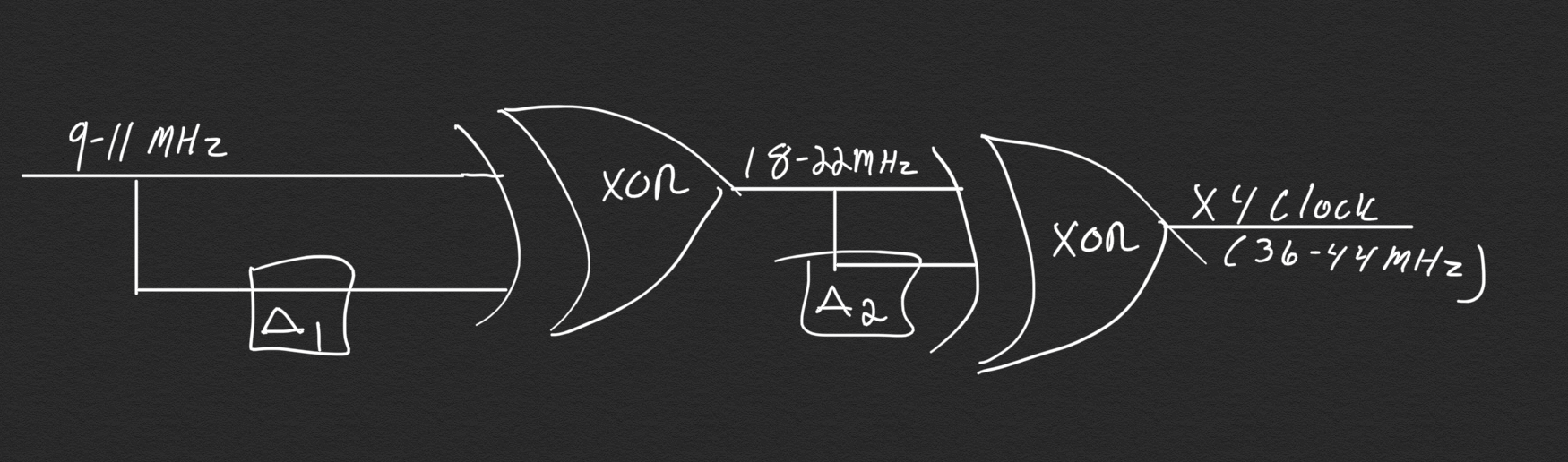
As seen below, we have our desired, higher level of abstraction schematic. We first input a 9-11 MHz clock signal into the first XOR gate in-series. In the second input of the first XOR gate, we have the delayed signal of the original 9-11 MHz clock signal. The output of the first XOR gate is a clock signal at 18-22 MHz. We take that output, and we delay it into the second input of the second XOR gate in-series. The overall desired result is a clock signal that is four times (36-44 MHz) the frequency of the original signal (9-11MHz).
Higher level of abstraction of our overall X4 clock frequency schematic |
|
| The fundamental equations used in our X4 frequency design | 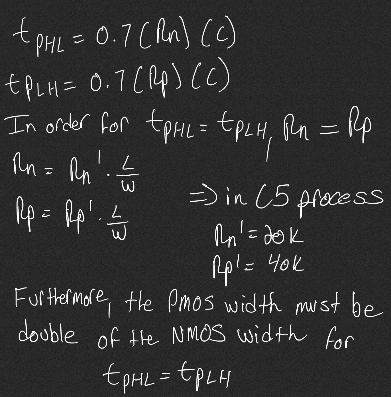 |
| Fundamental concept in designing the inverter widths and lengths to accomodate proper delays throughout our entire project | 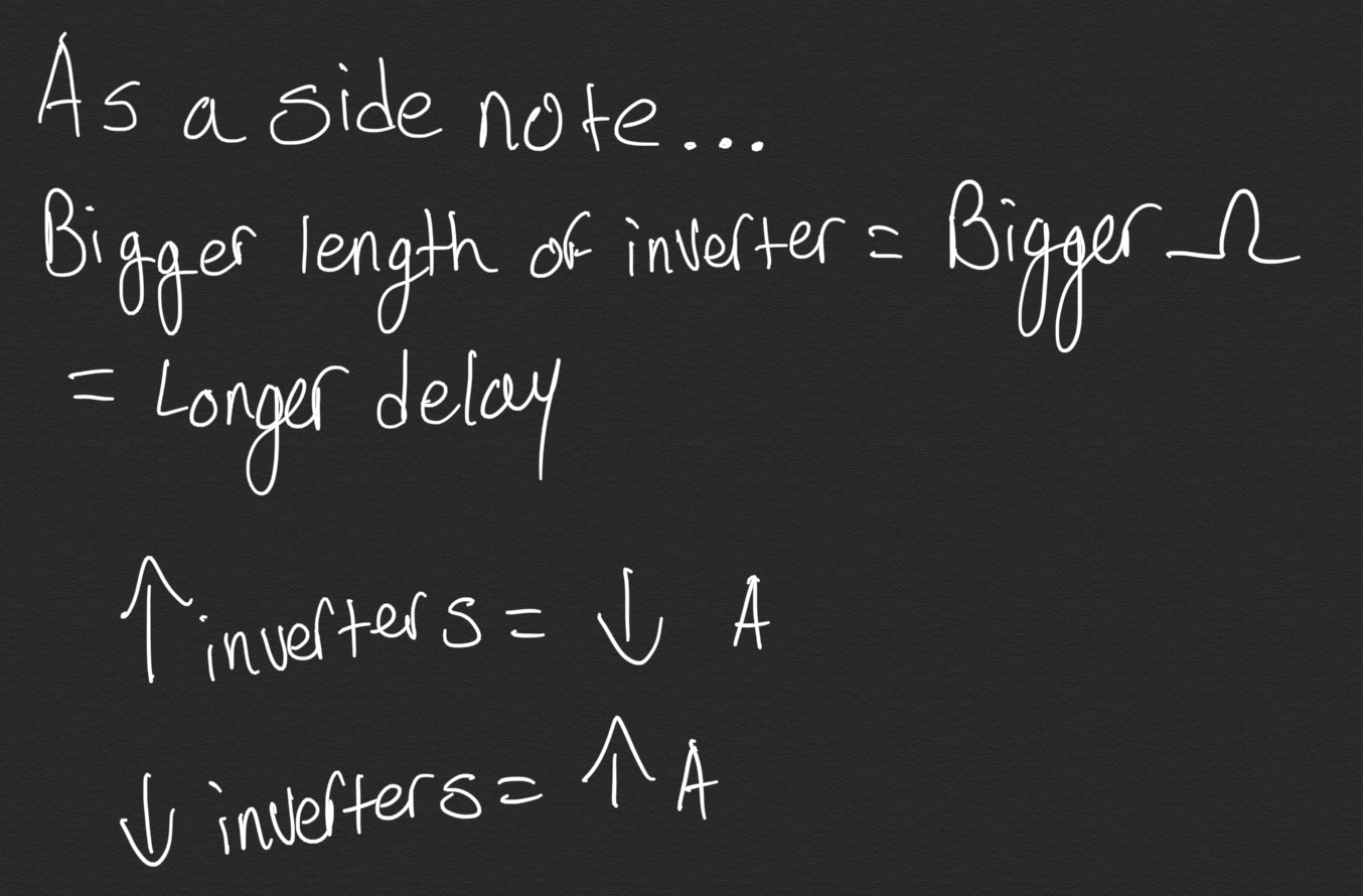 |
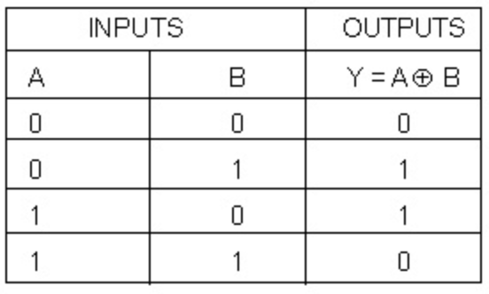
| An XOR gate should operate as seen below in the truth table |
|
Given we will be utilizing XOR gates throughout this project, we instantiated the XOR cell view into our lab project library. Below, we have the schematic for our XOR gate. | 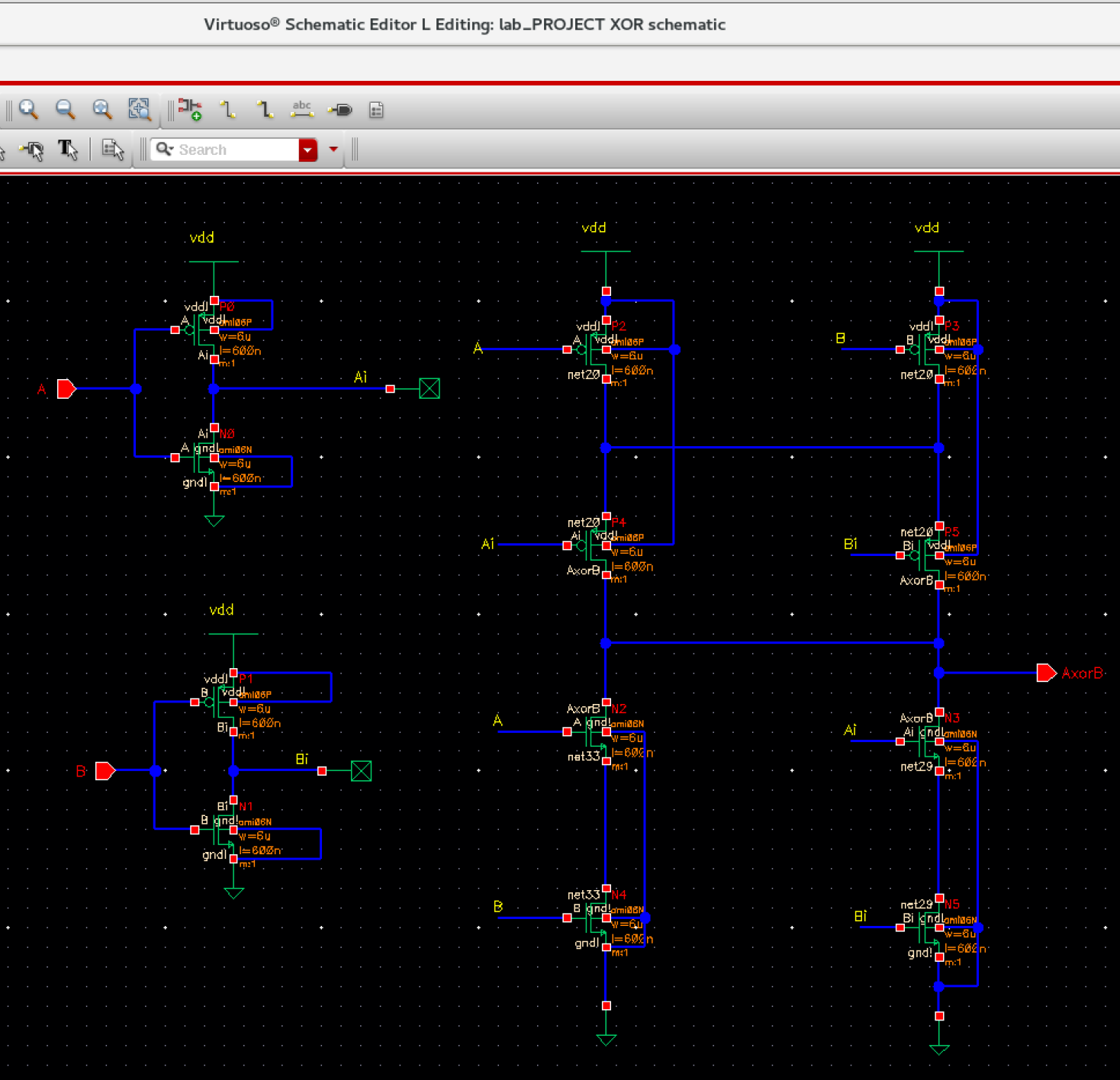 |
| This is our symbol for our XOR gate | 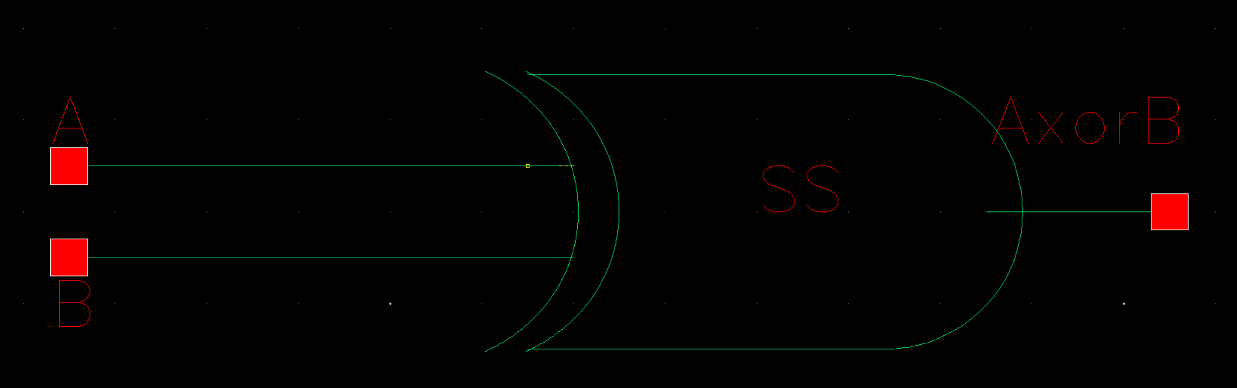 |
| This is our simulation schematic for our XOR gate utilizing pulse signals | 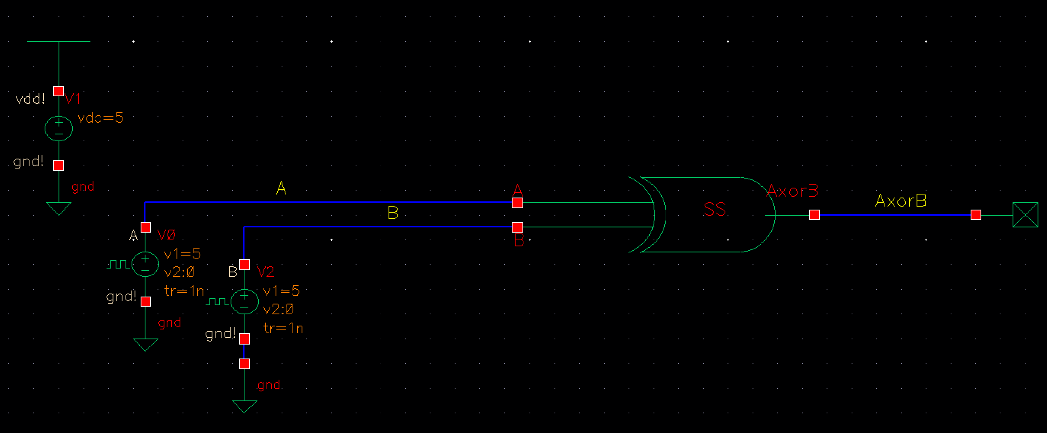 |
| This is our simulation results of our XOR gate utilized in our project | 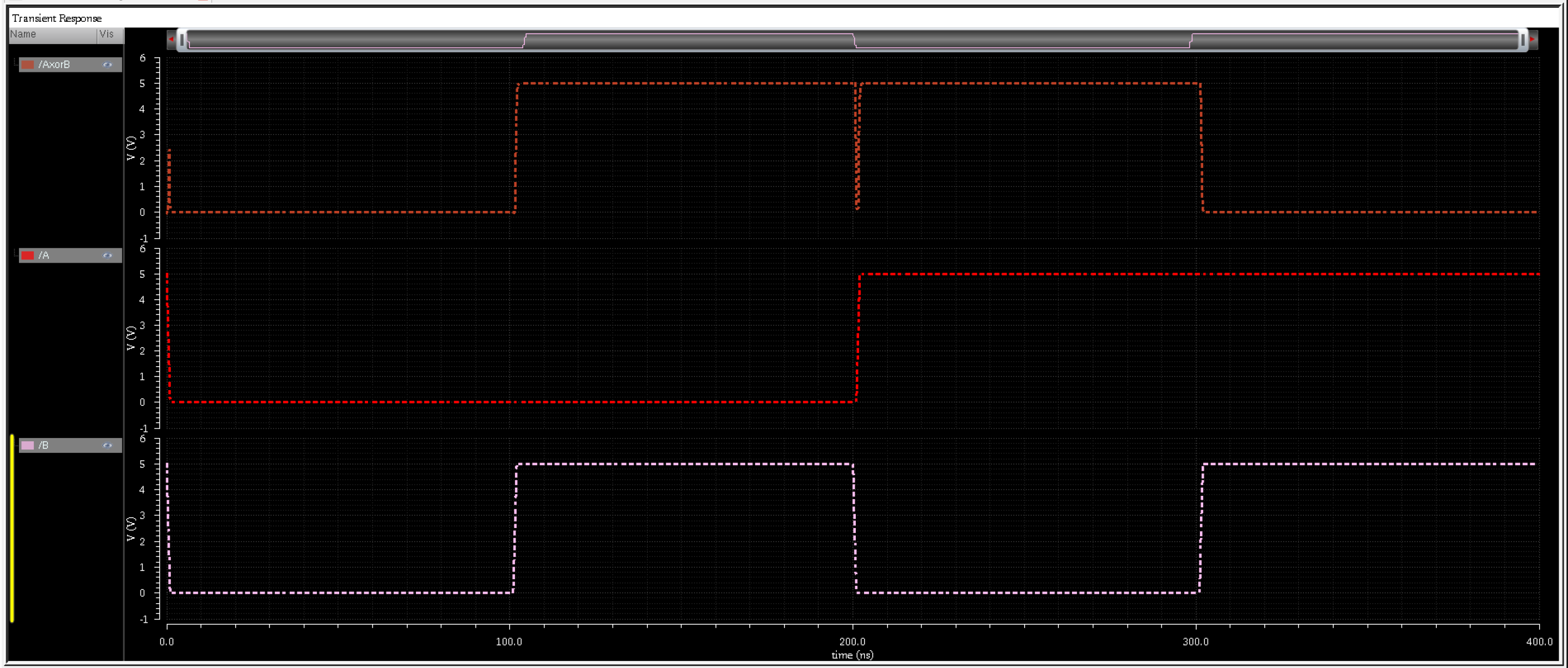 |
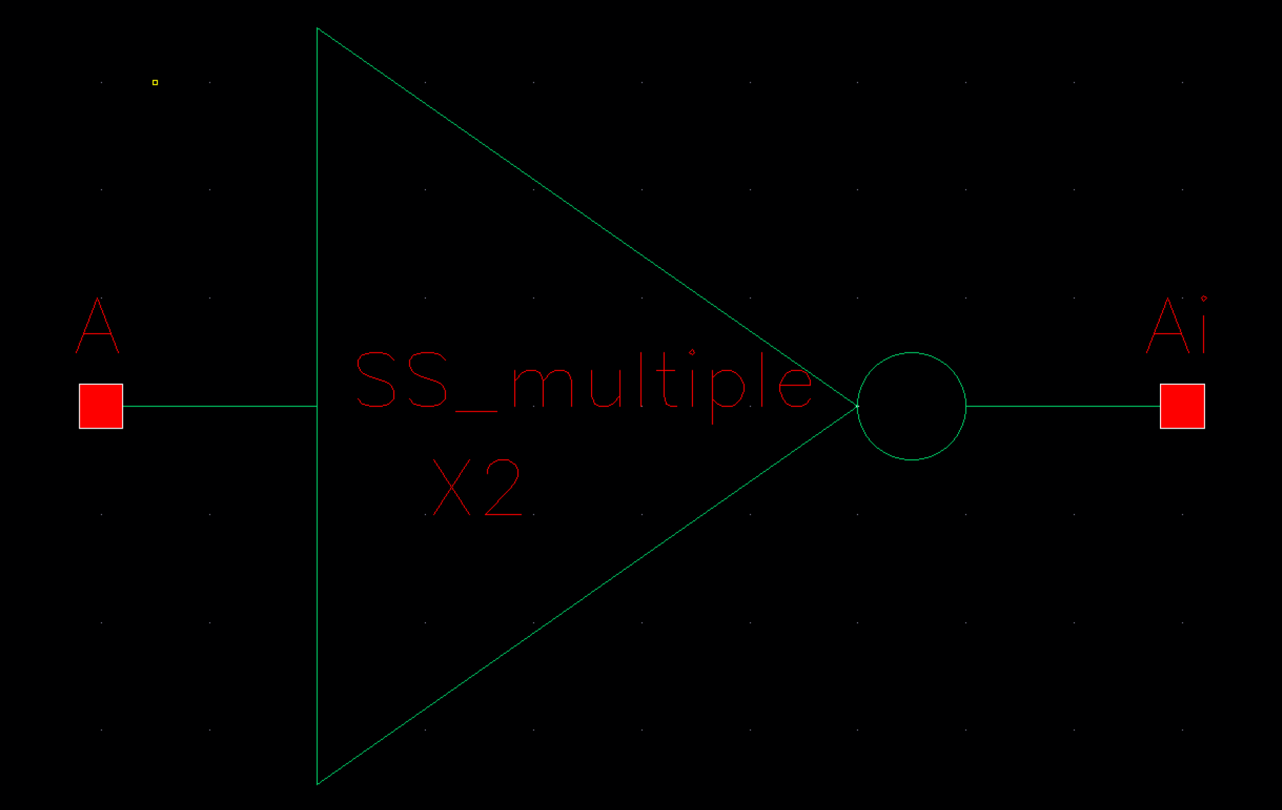
| Here is the symbol view for our X2 clock inverter string |
|
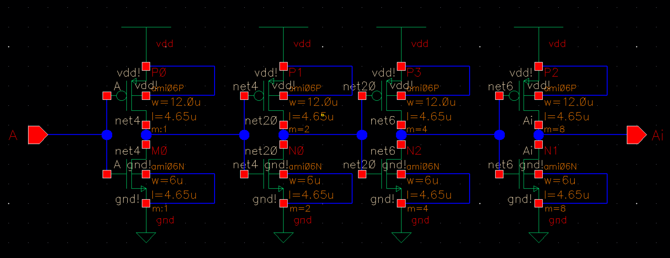
Here is our schematic view for our X2 clock inverters |
|
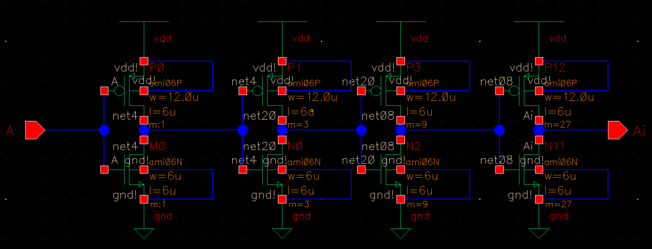
Here is our symbol view for our X4 clock inverters string | 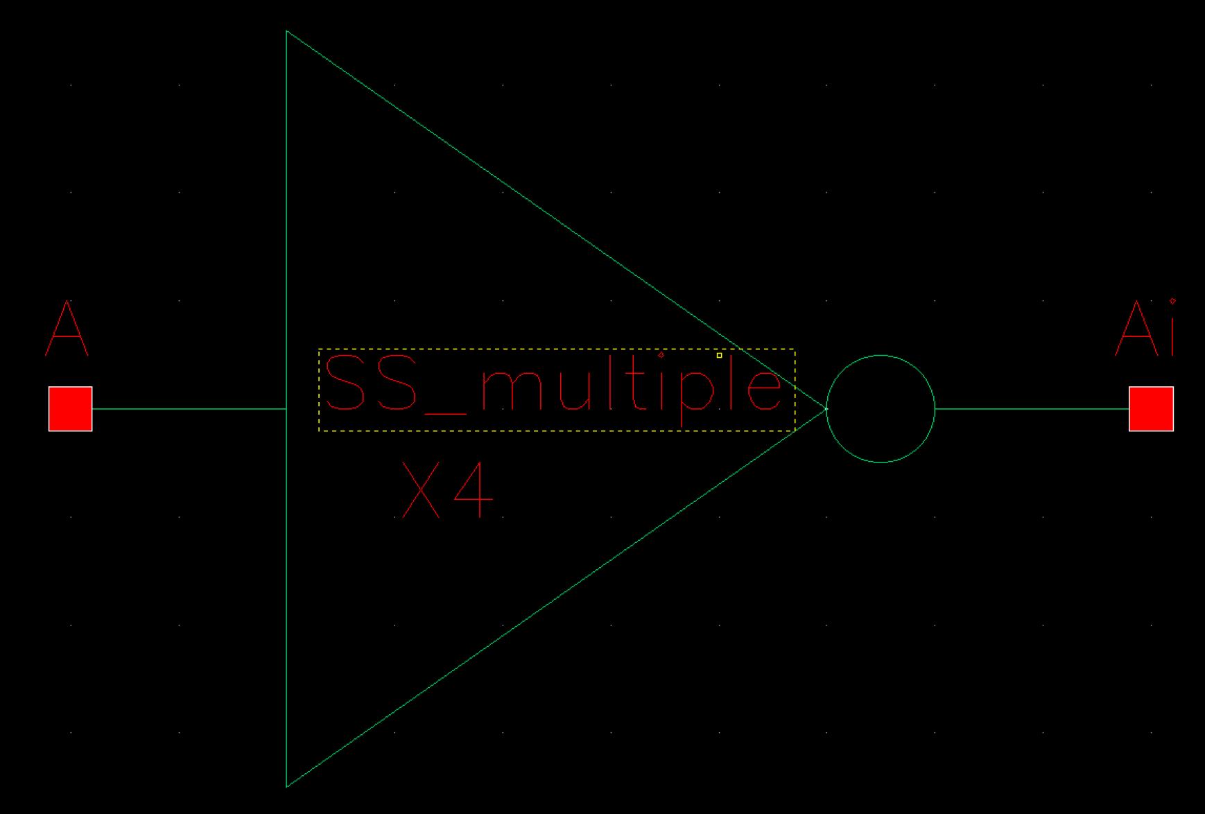 |
This is our schematic for our X4 clock inverters string |
|
Here is our symbol for our square-up inverters | 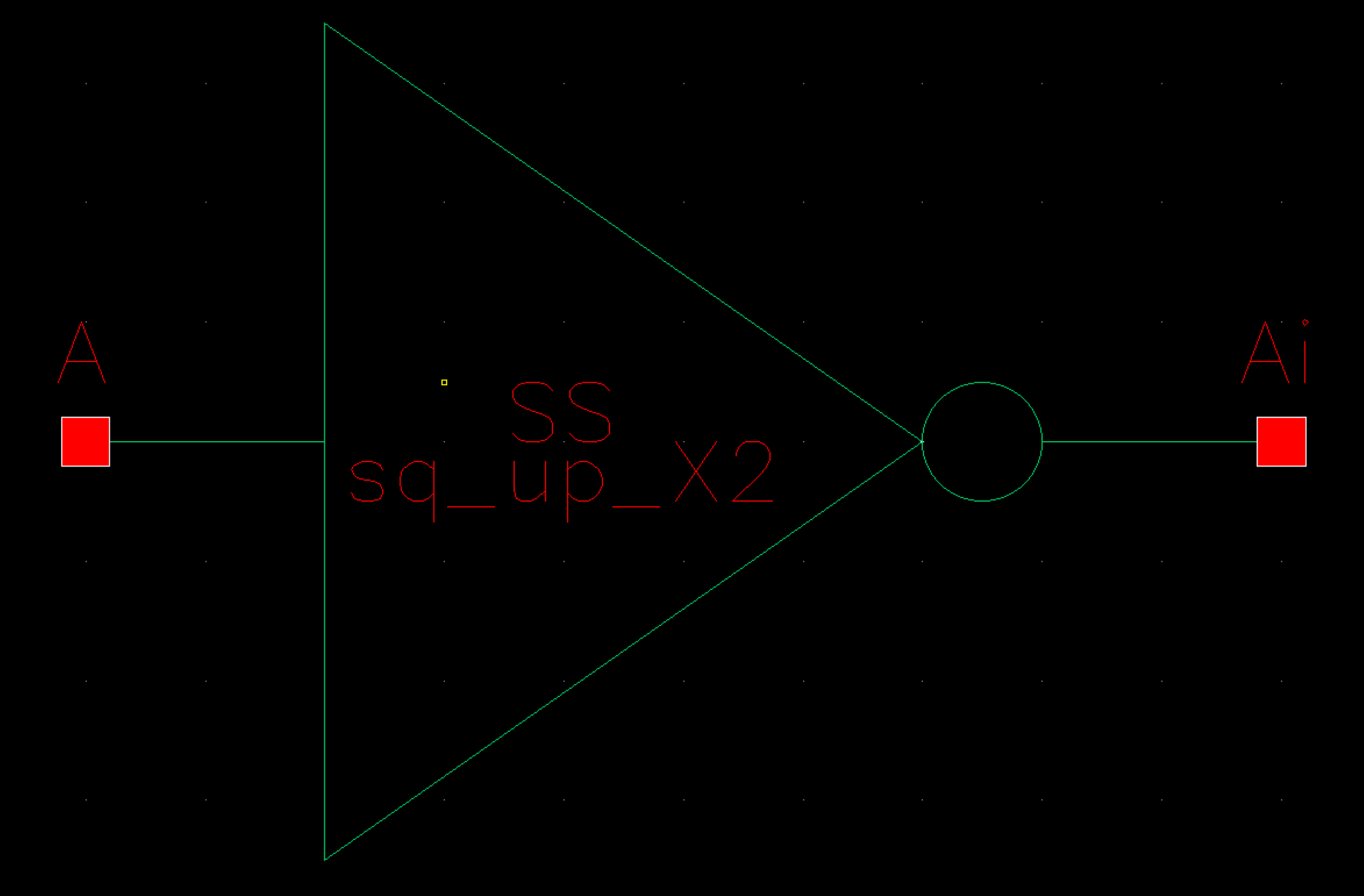 |
Here is the schematic for our square-up inverters that are used to make our signals have a sharper edge | 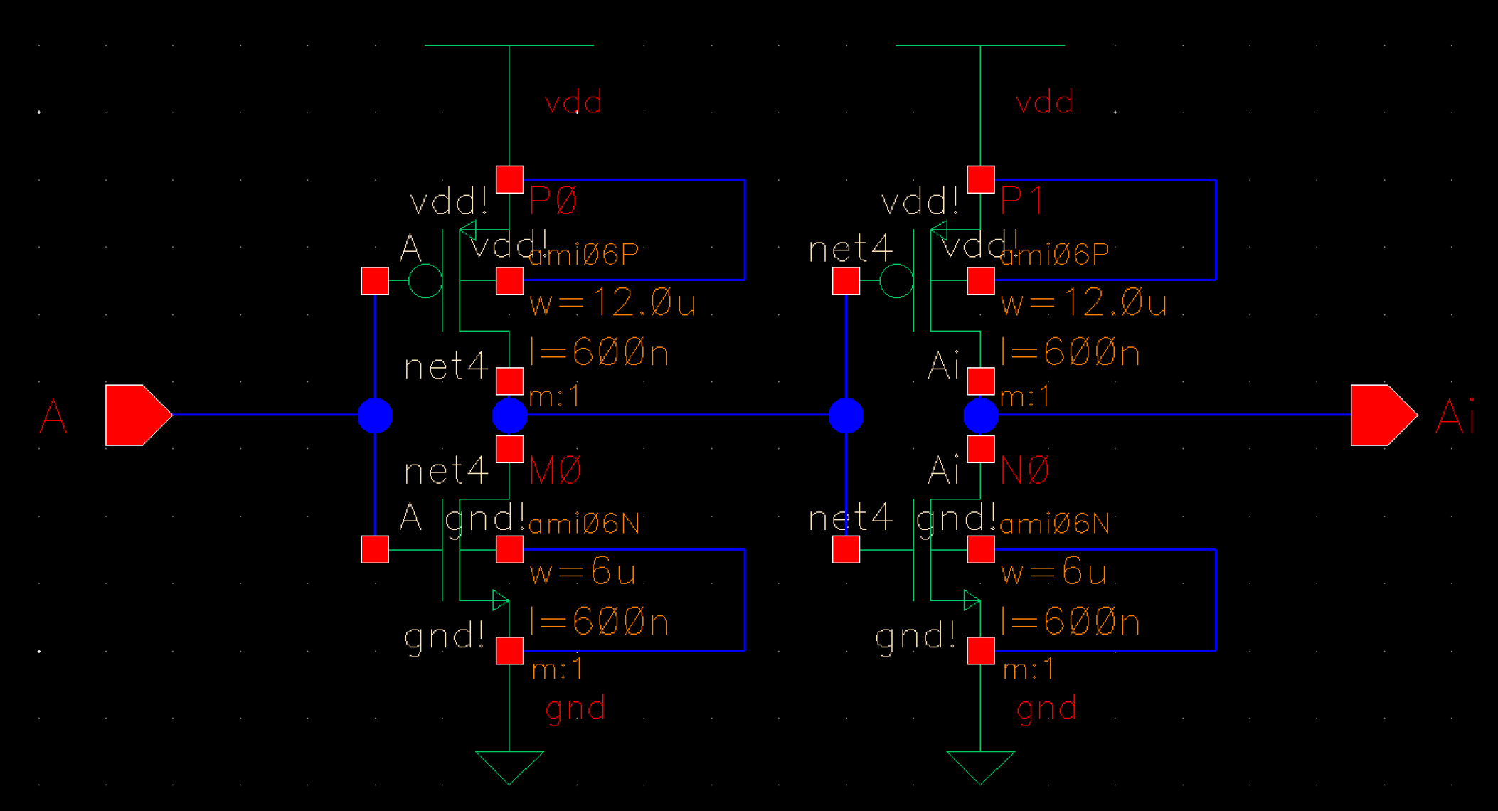 |
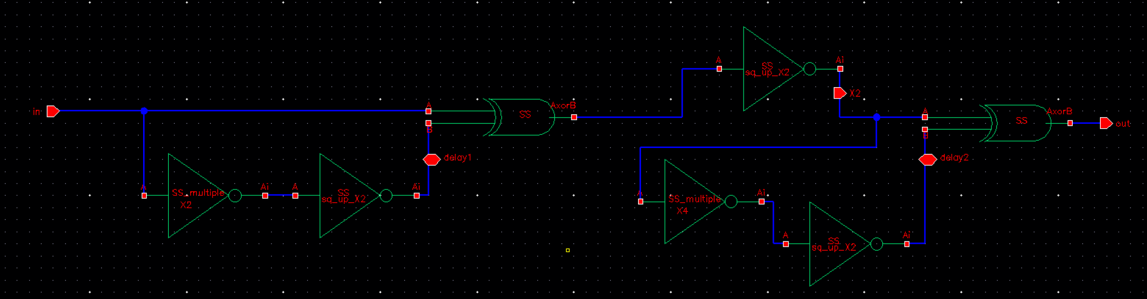
Overall final schematic of our X4 Clock multiplier |
|
Running our simulations at different VDC and frequency values
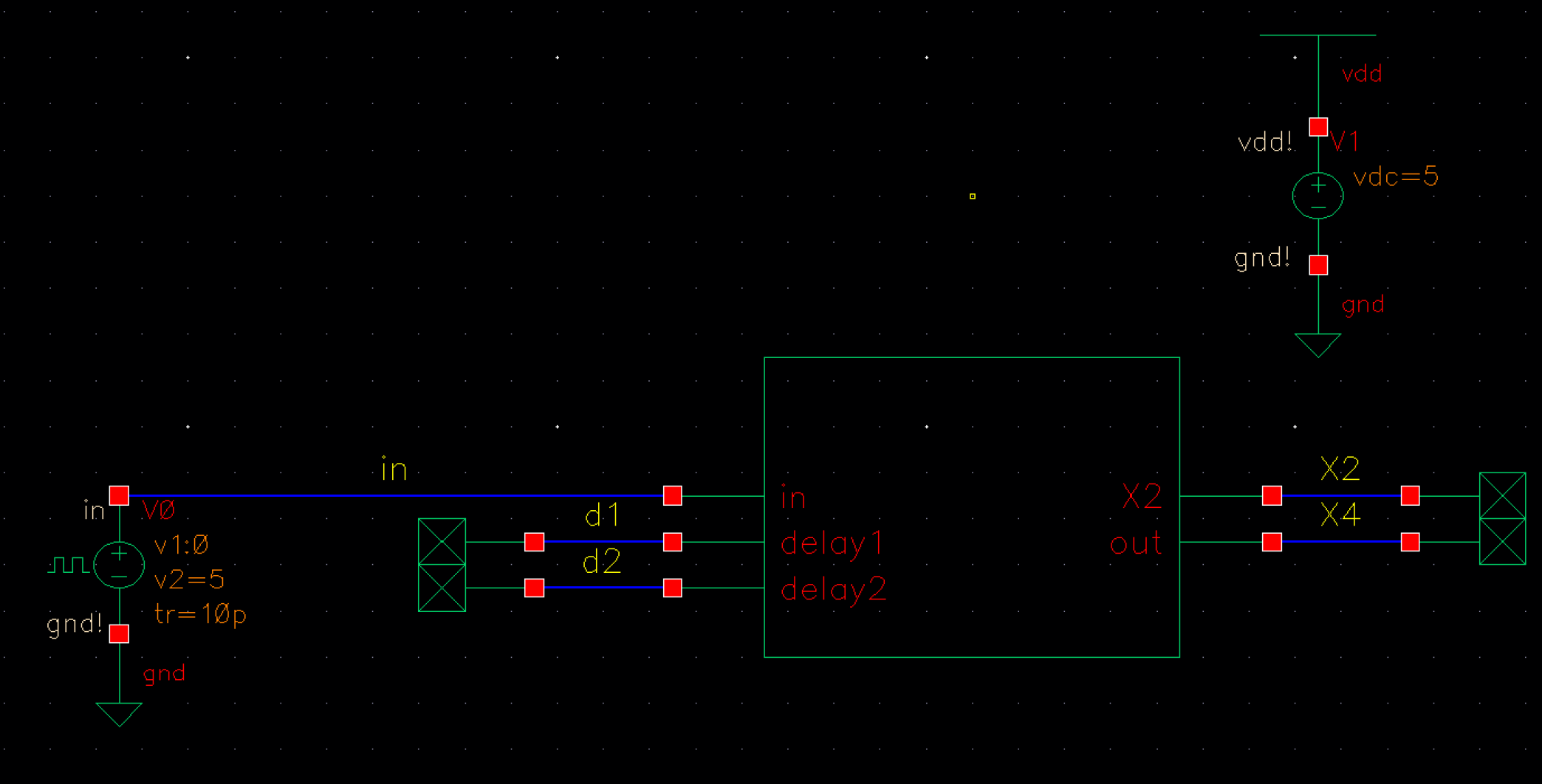
Here, we have our overall simulation schematic of our overall X4 clock multiplier. From this view, we are at a higher level of abstraction of our overall scheamtic (black box representation). Notice our pulse signal, VDD, delay 1/2, and X2/X4 pins below. |
|
| 9MHZ @ 4VDC | 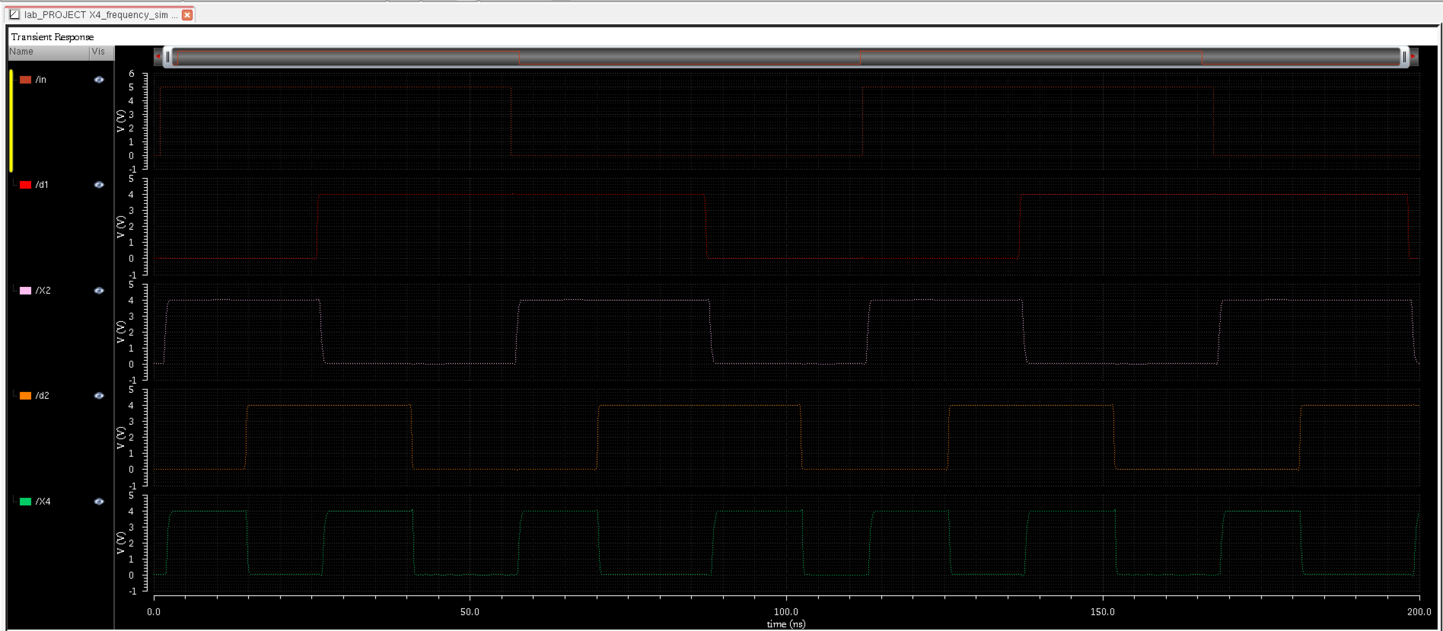 |
| 9MEG @ 5VDC | 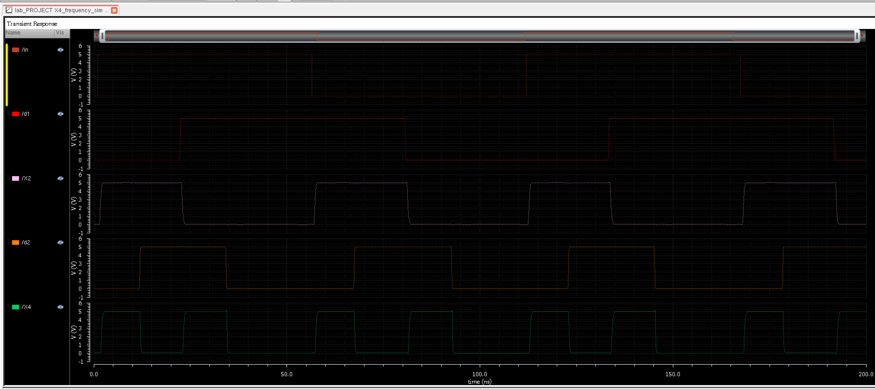 |
| 9MEG @ 6VDC | 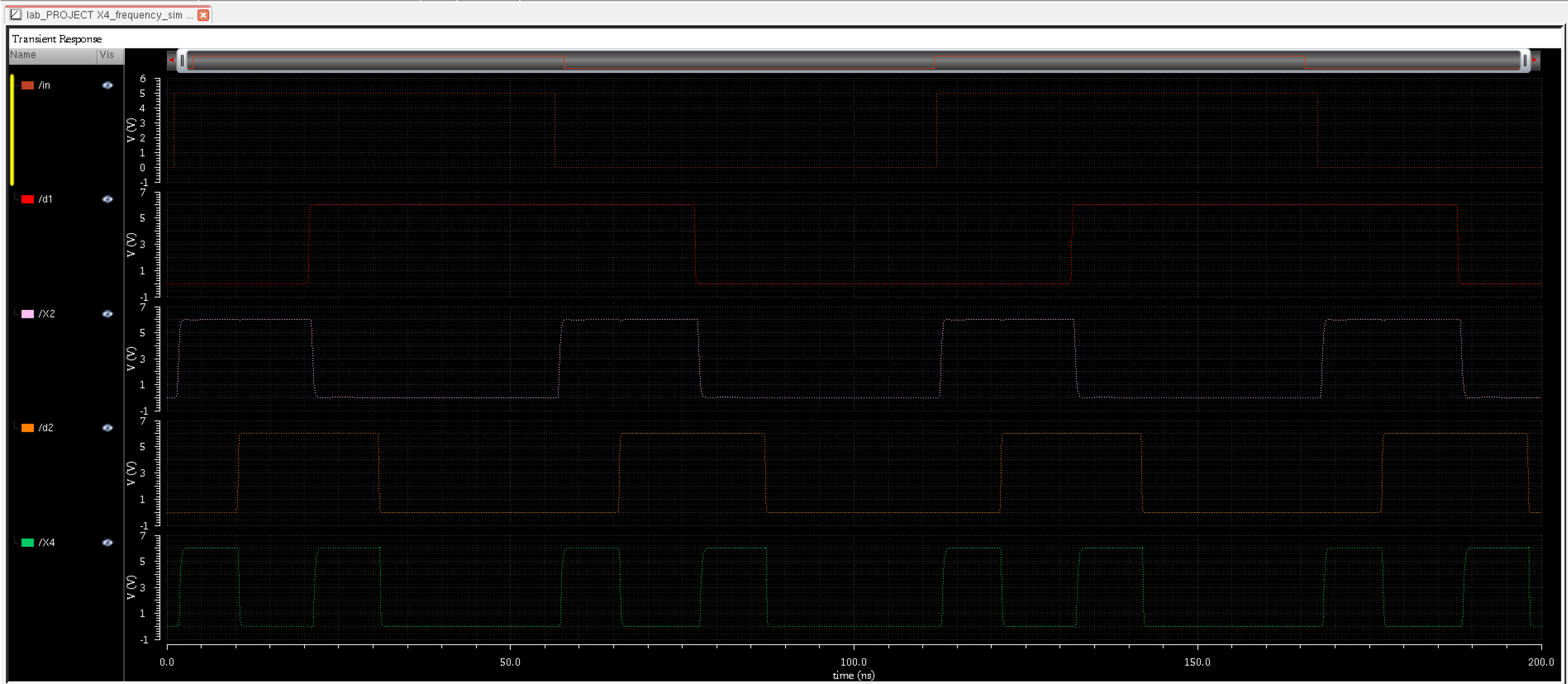 |
| 10MEG @ 4VDC | 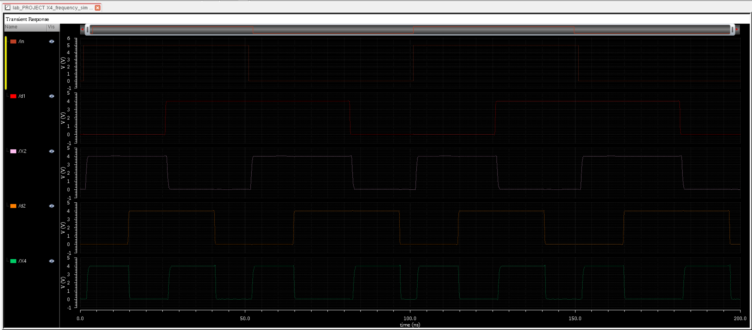 |
10MEG @ 5VDC | 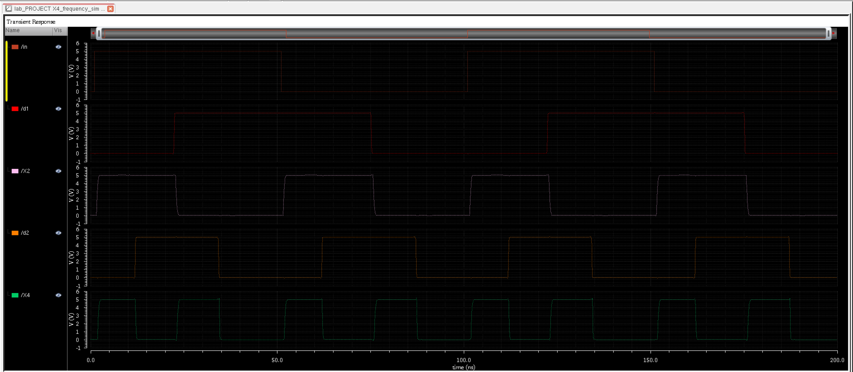 |
| 10MEG @ 6VDC | 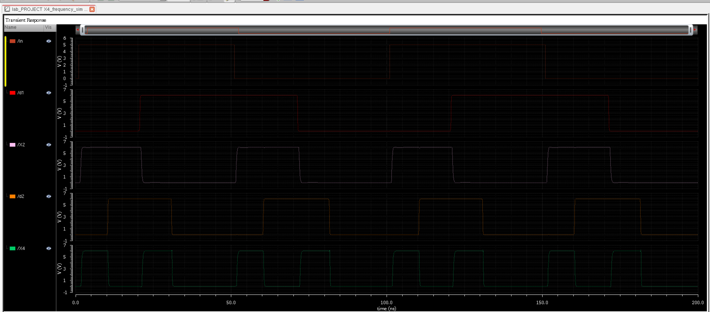 |
| 11 MEG @ 4VDC | 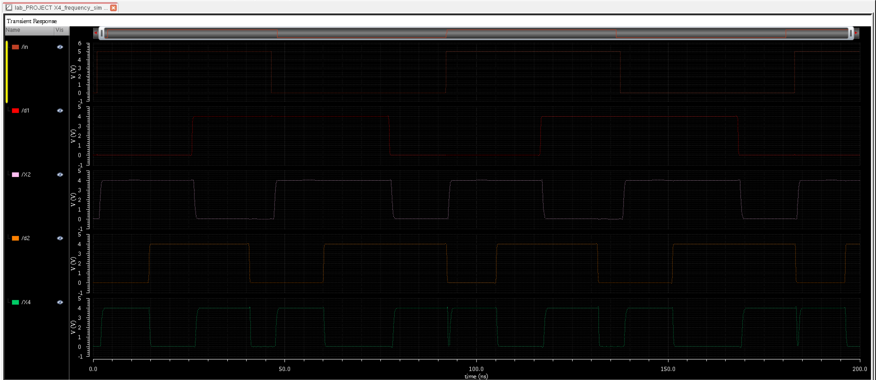 |
| 11 MEG @ 5VDC | 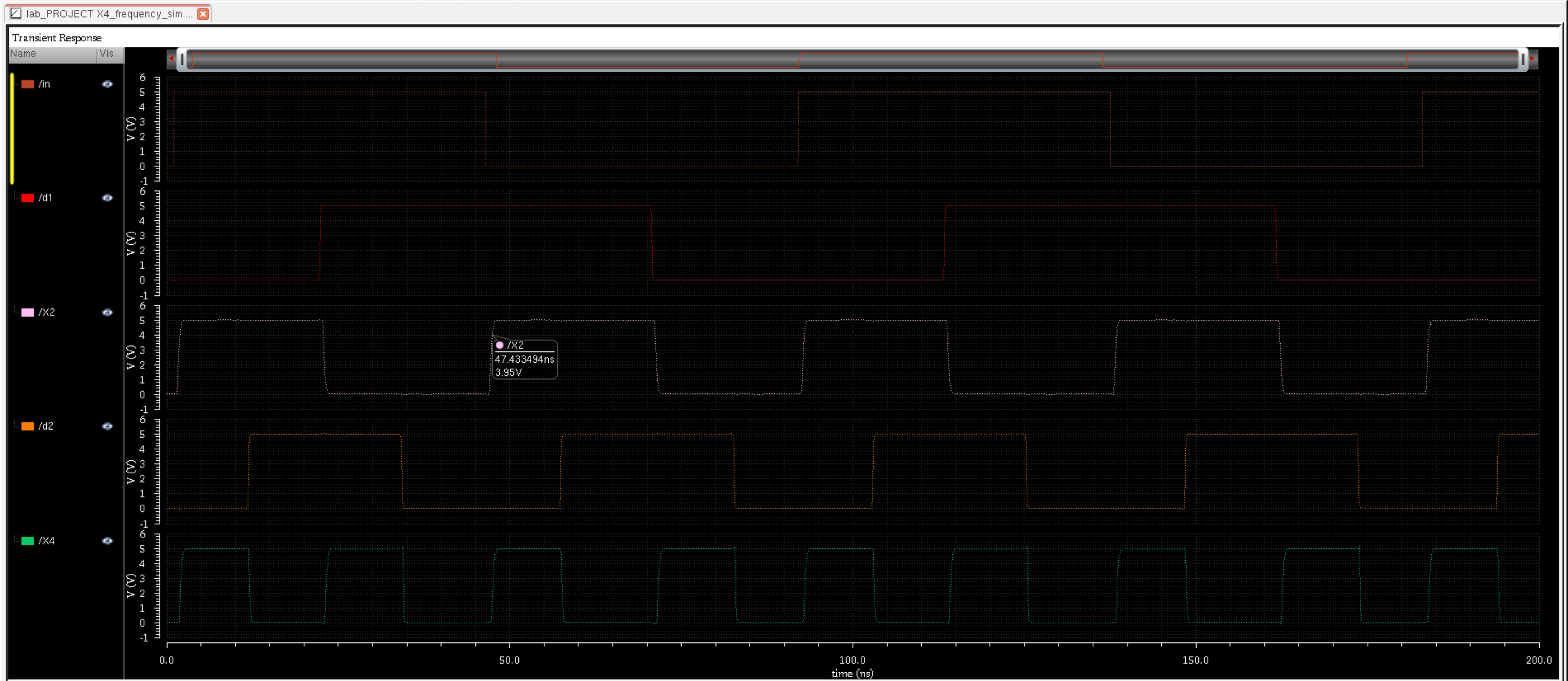 |
| 11 MEG @ 6VDC | 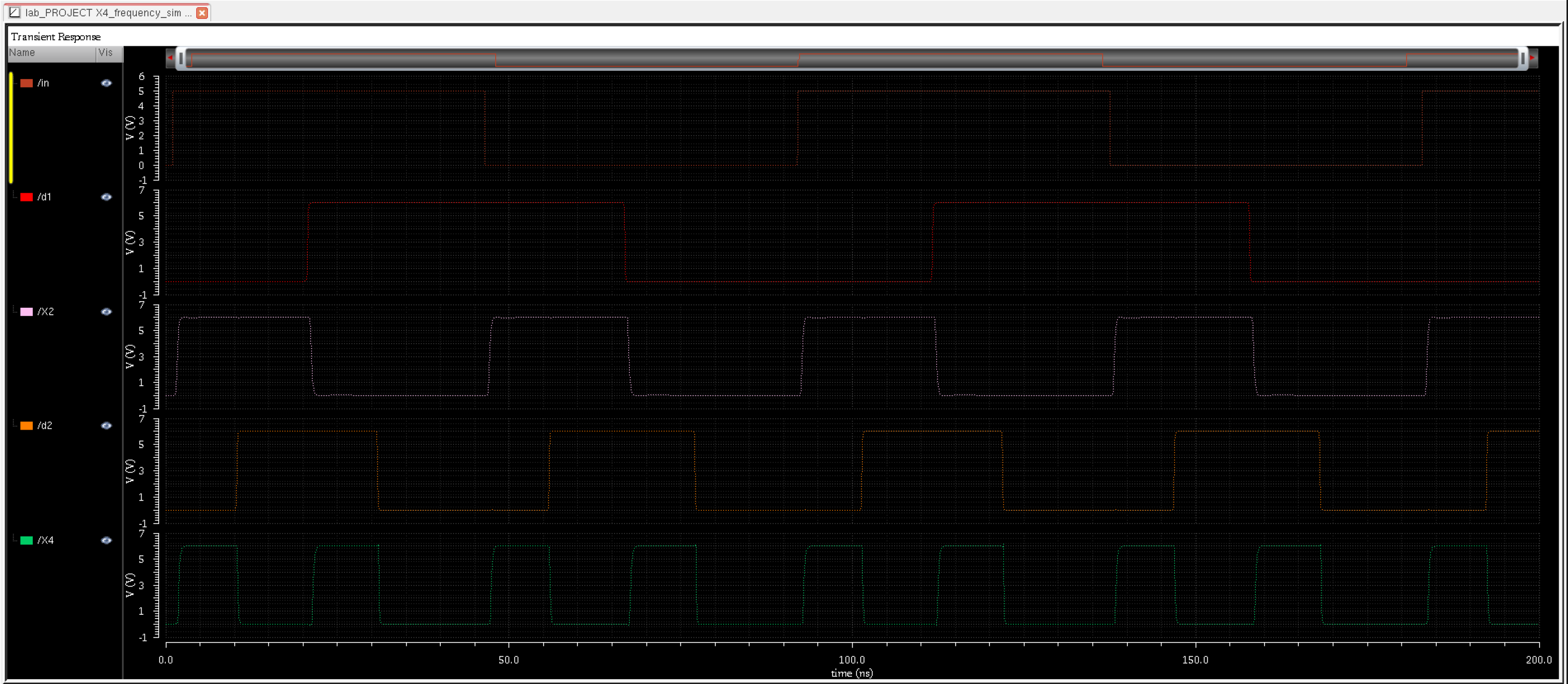 |
| XOR Layout Cell View | 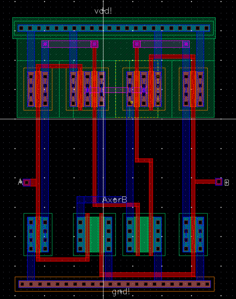 |
| Our XOR gate underwent DRC check nicely | 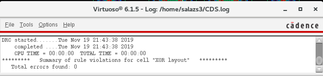 |
| Our XOR gate extracted view with LVS verification in the cell view | 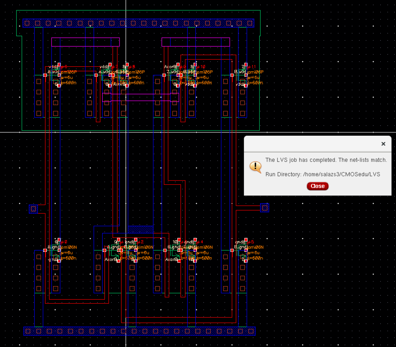 |
| Additional verification that our XOR gate layout cell view underwent LVS with a proper net-list check | 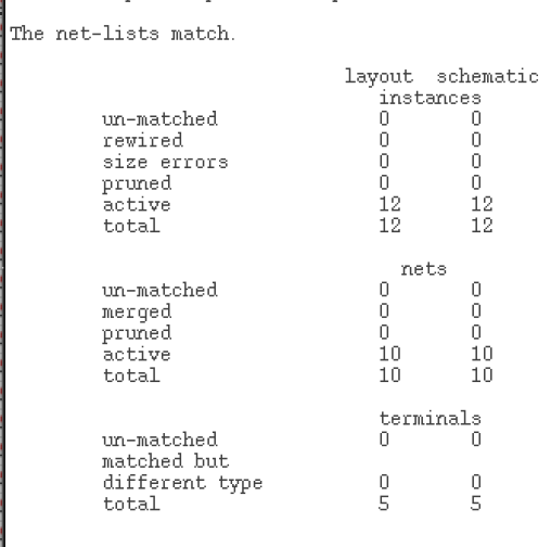 |
| Here is our layout view for our inverters used to "square-up" our internal signals | 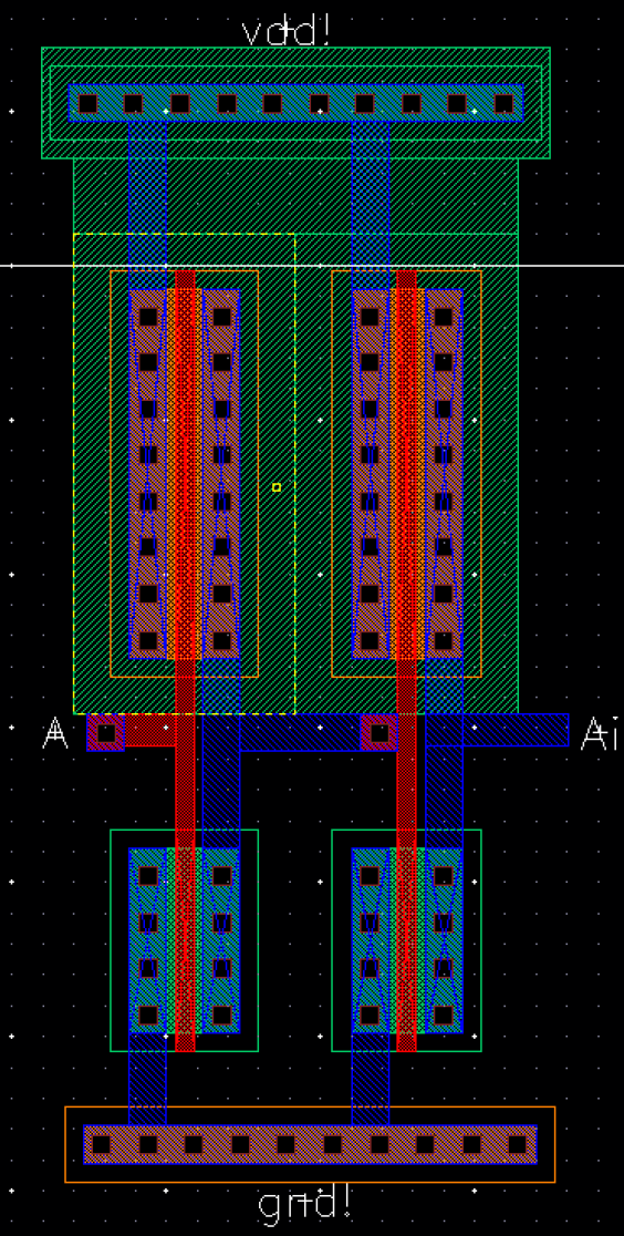 |
| This shows our "square-up" inverter layout cell view underwent DRC check nicely... | 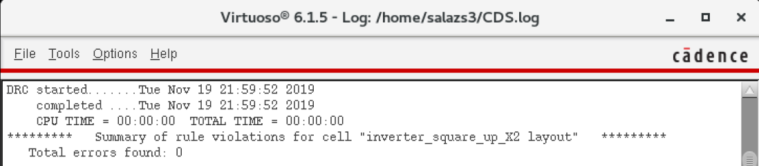 |
| Here is our extracted view of our "square-up" inverters with accompanying LVS verification for safe measures... | 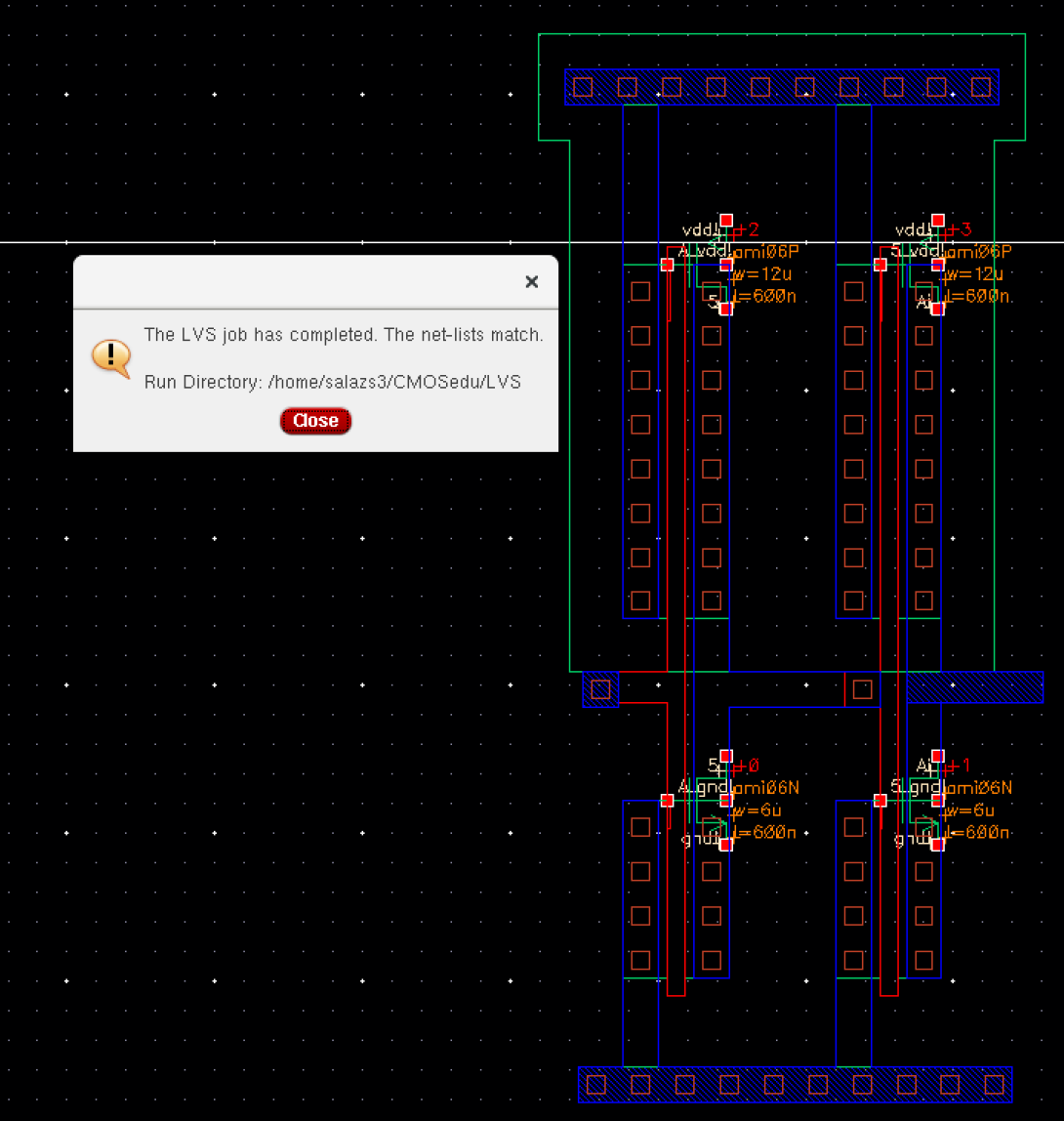 |
| Additional net-lists verifications of our "square-up" inverters | 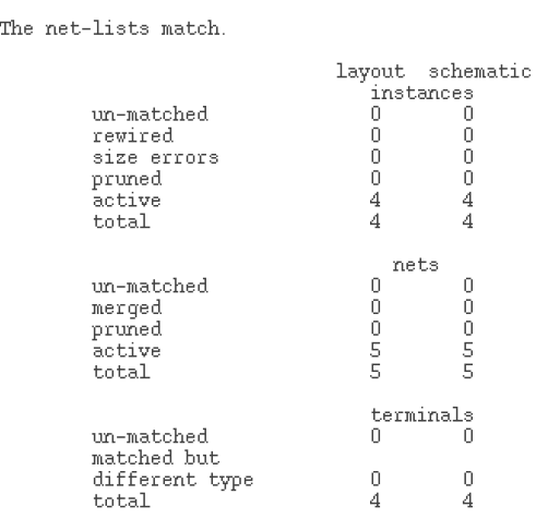 |
| Overall layout of our inverter multiple X2 frequency cell view | 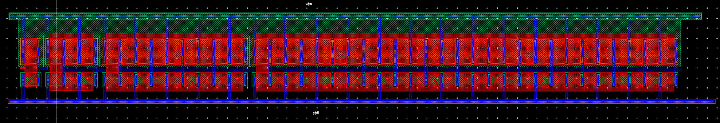 |
| Zoomed-in view of the extreme right-side of the layout of the X2 frequency inverter string | 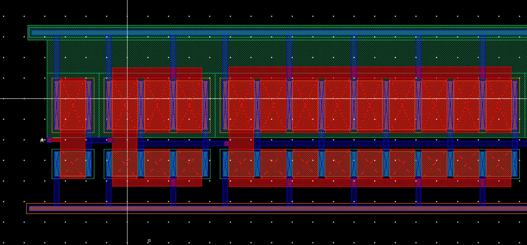 |
| Zoomed-in view of the extreme left-side of the layout of the X2 frequency inverter string | 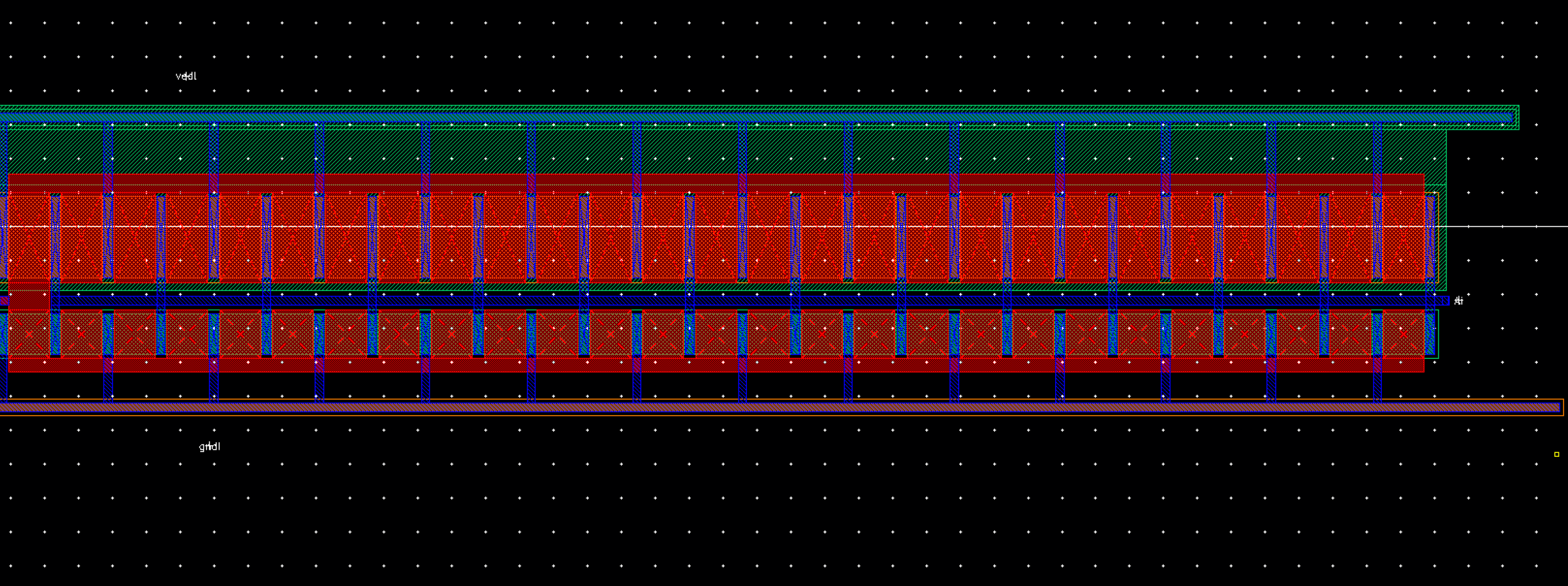 |
| We made sure this layout underwent DRC nicely.. | 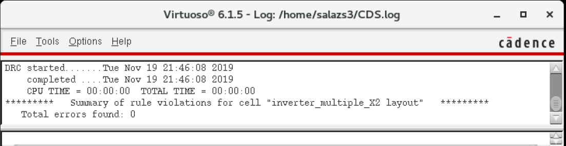 |
| Extracted cell view of our X2 frequency inverter string also verifying LVS | 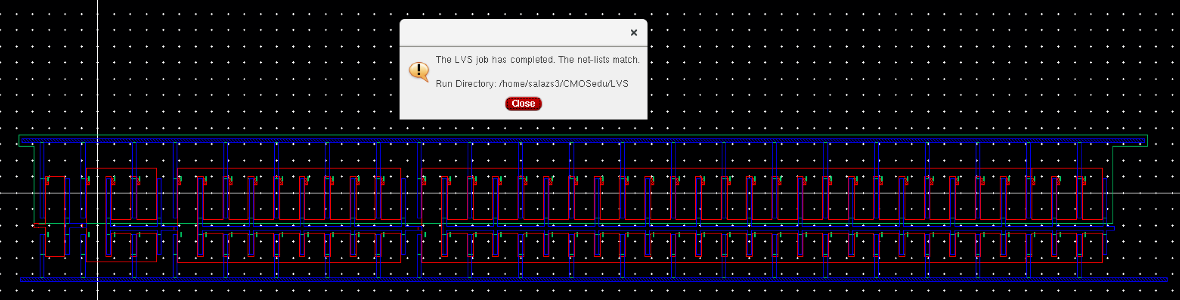 |
| Additional LVS verification of our X2 frequency inverter string | 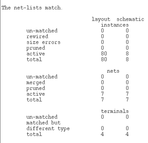 |
| Here is the X4 frequency inverter string layout cell view | 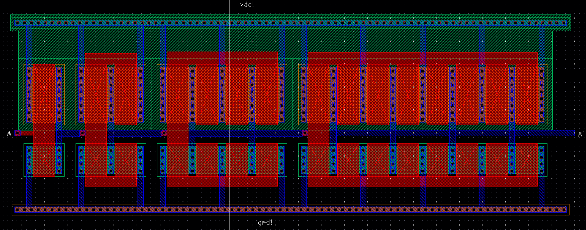 |
| Here is the DRC verification of our X4 frequency inverter string | 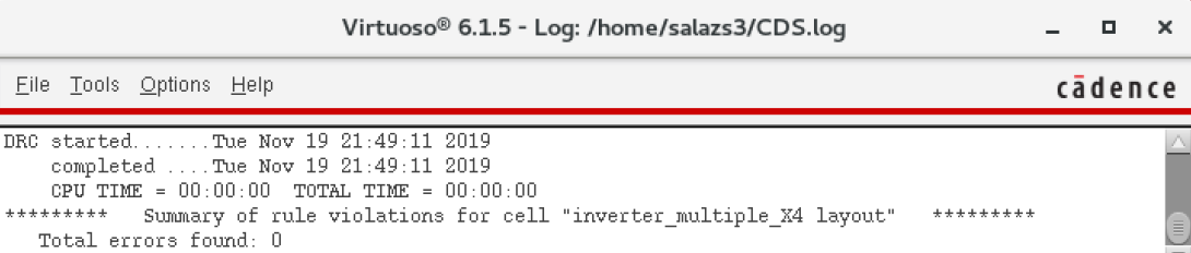 |
| Here is the extracted view/LVS verification of our X4 frequency inverter string | 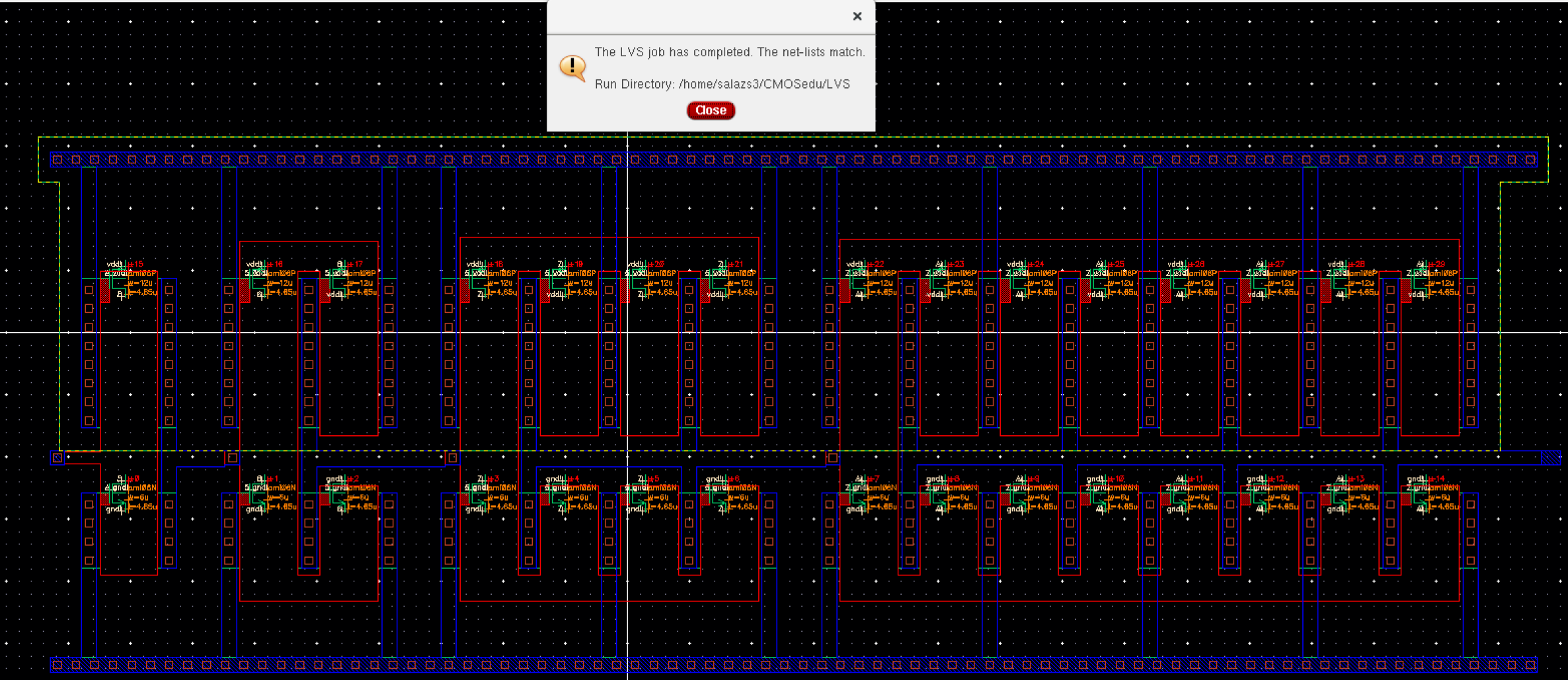 |
| Here is the additional LVS verification of our X4 frequency inverter string | 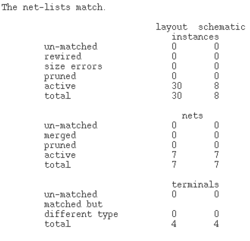 |
| Overall layout of our X4 frequency design | 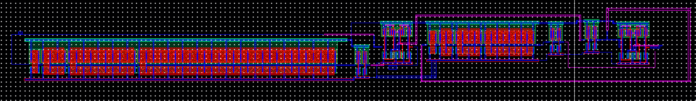 |
| DRC verification of our X4 frequency layout | 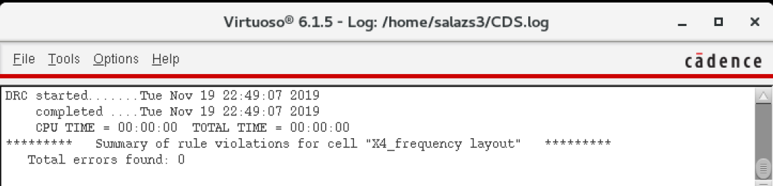 |
| Left zoomed-in side (X2 string inverters) of overall X4 frequency layout | 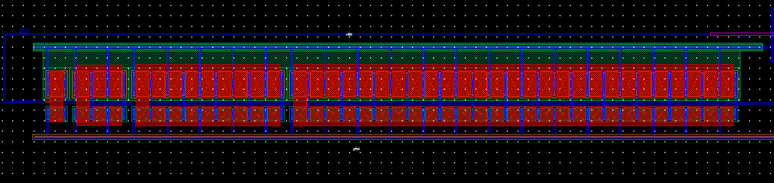 |
| Square-up inverters and first XOR gate (left to right) of X4 frequency layout | 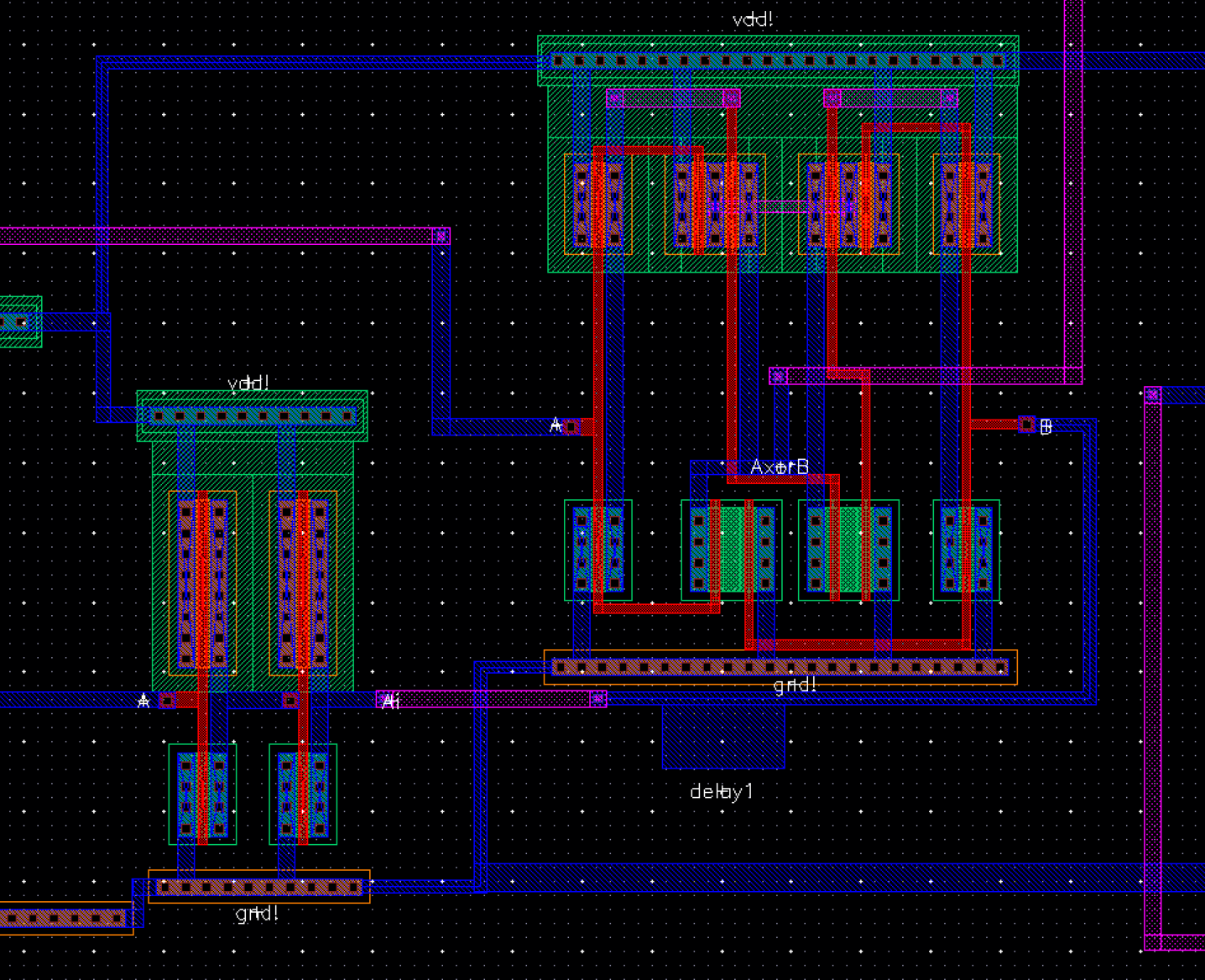 |
| Looking at the second half (X4 inverter string, square up inverters, and XOR gate) of X4 frequency layout | 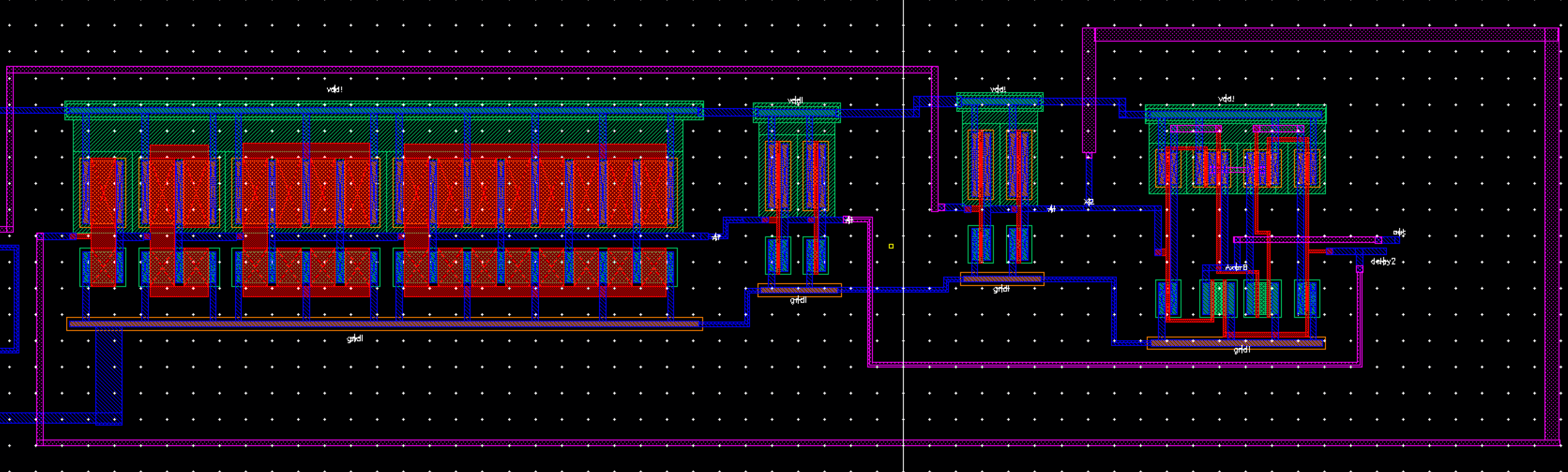 |
| Zoomed-in view of second half (left to right) of X4 frequency layout | 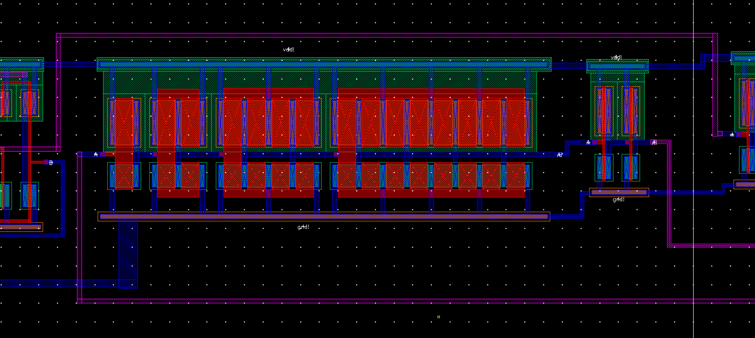 |
| Extreme right side view of X4 frequency layout | 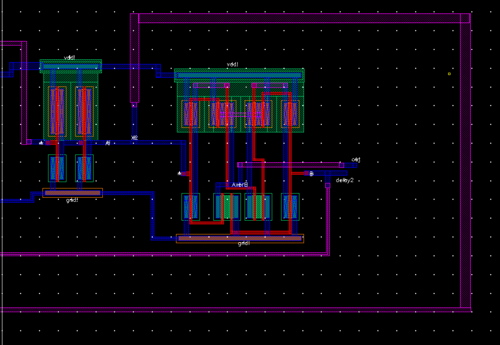 |
| LVS Verification of X4 frequency layout | 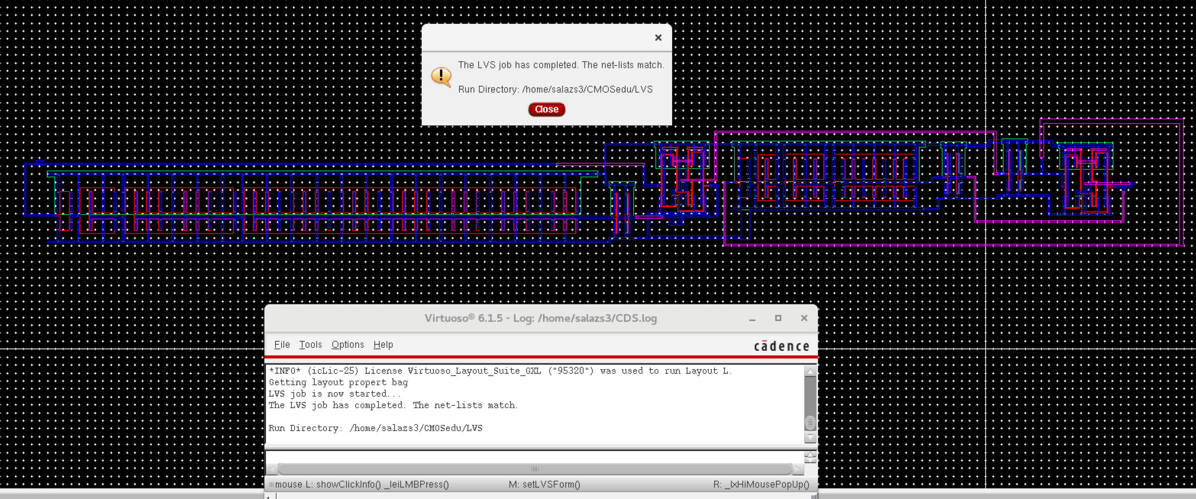 |
| Additional LVS Verification of X4 frequency layout | 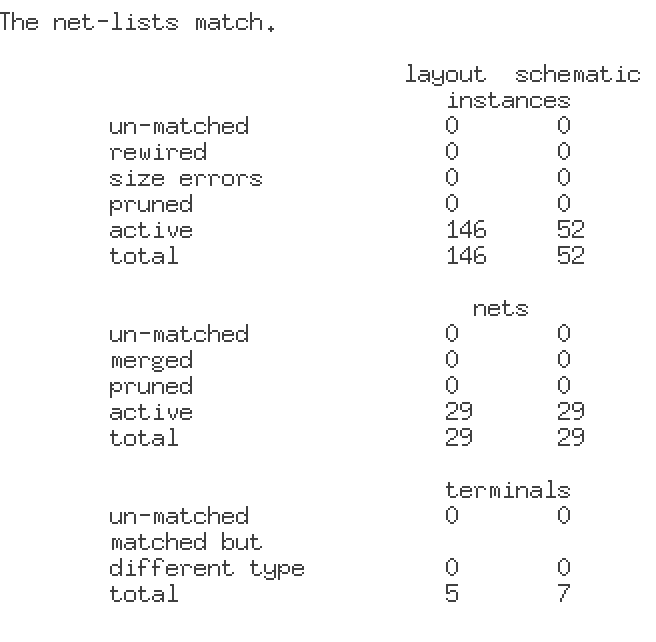 |