Lab 7 - EE 421L
Authored
by Steve Salazar Rivas
Email: salazs3@unlv.nevada.edu
November 6th, 2019
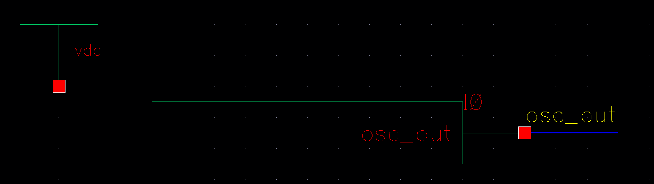
Prelab: For lab 7, we went through Tutorial 5 where we designed a ring oscillator.
Actual Lab 7:
First, we created the schematic for our inverter with a four bit input and output, respectively.
This is our corresponding inverter symbol...
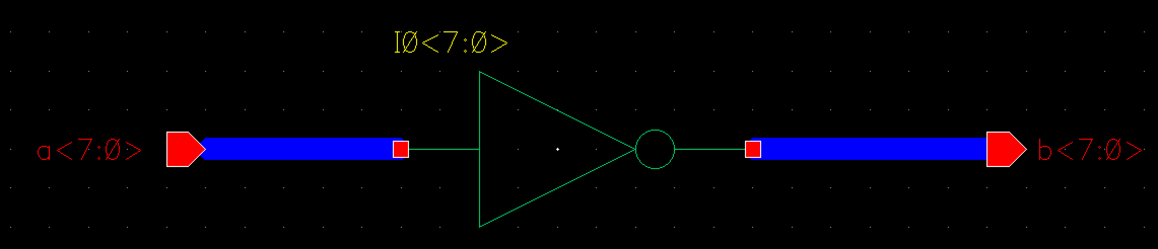
This is our simulation schematic for our four bit inverter...

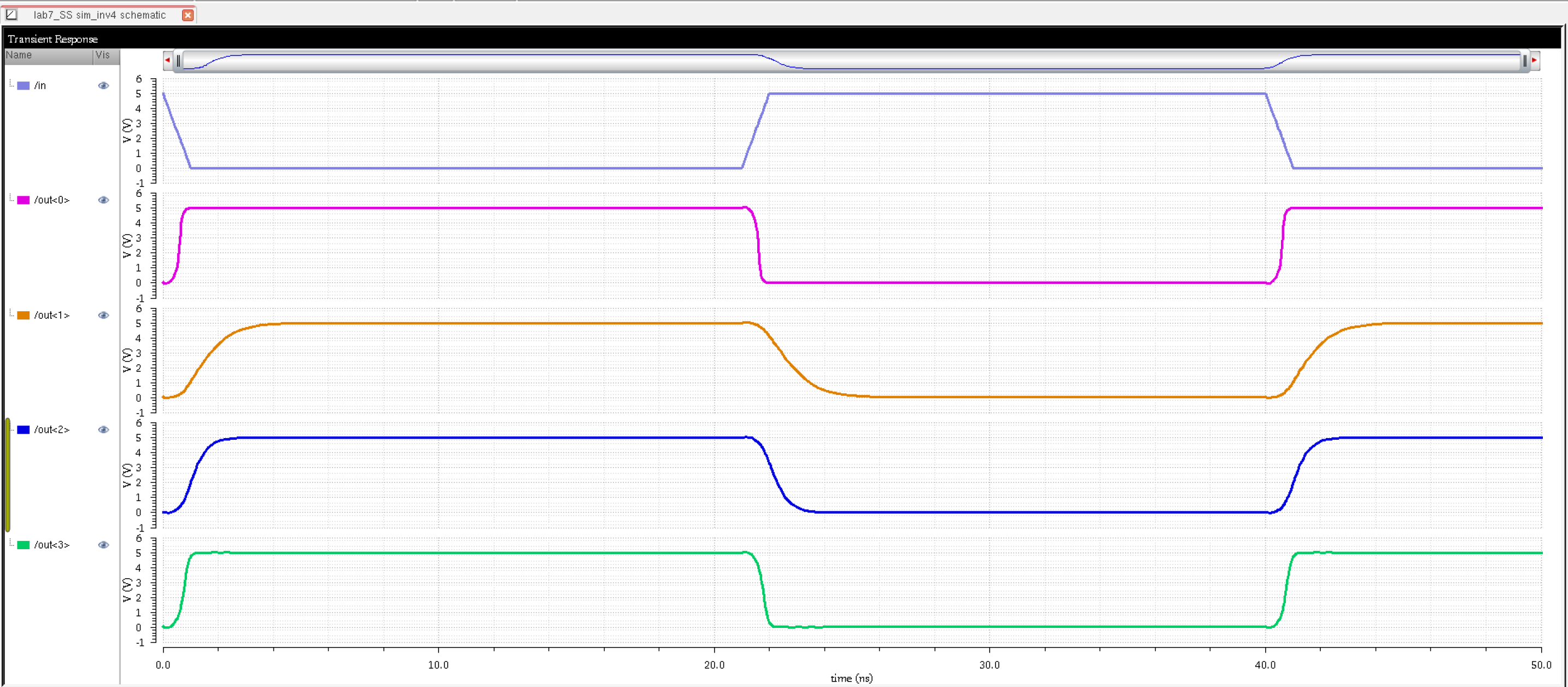
Here is our simulation results of our inverter that is driving the corresponding capacitors and with an input pulse source.
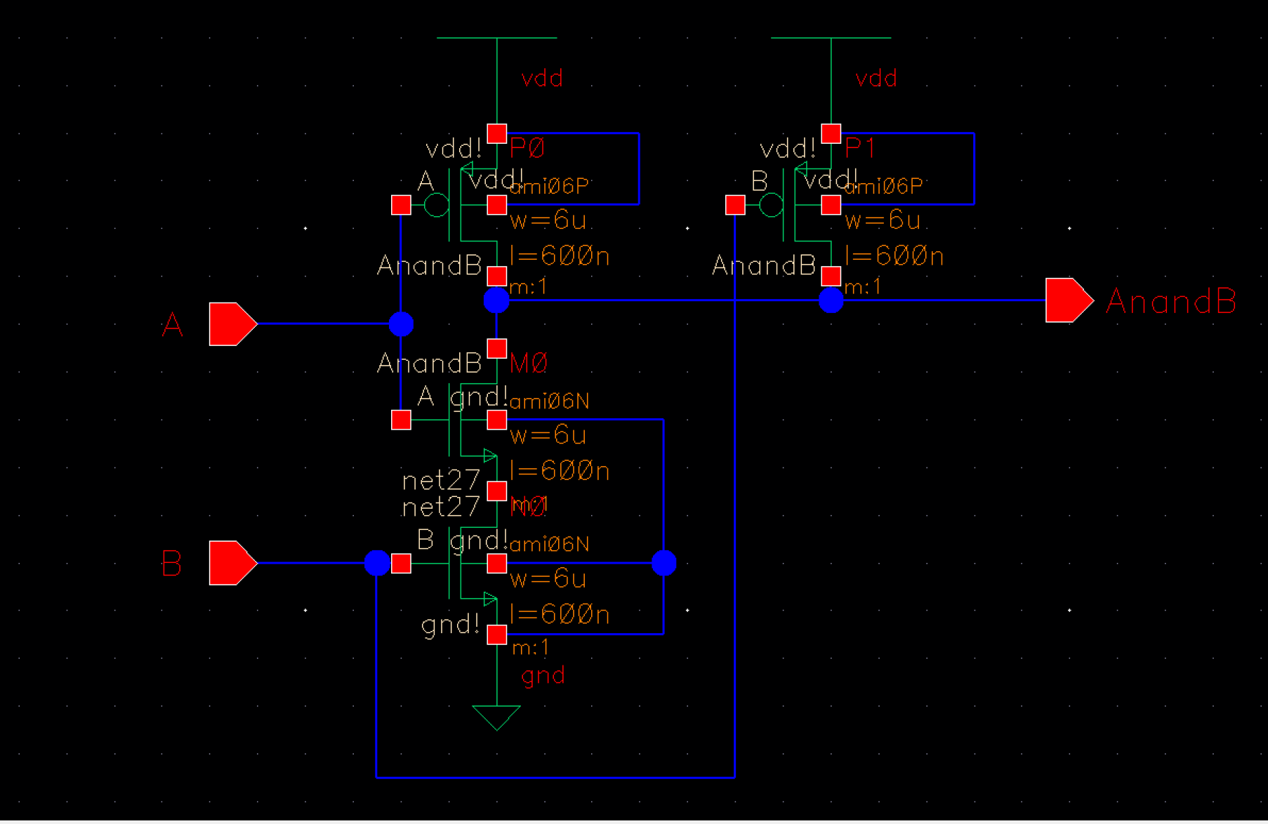
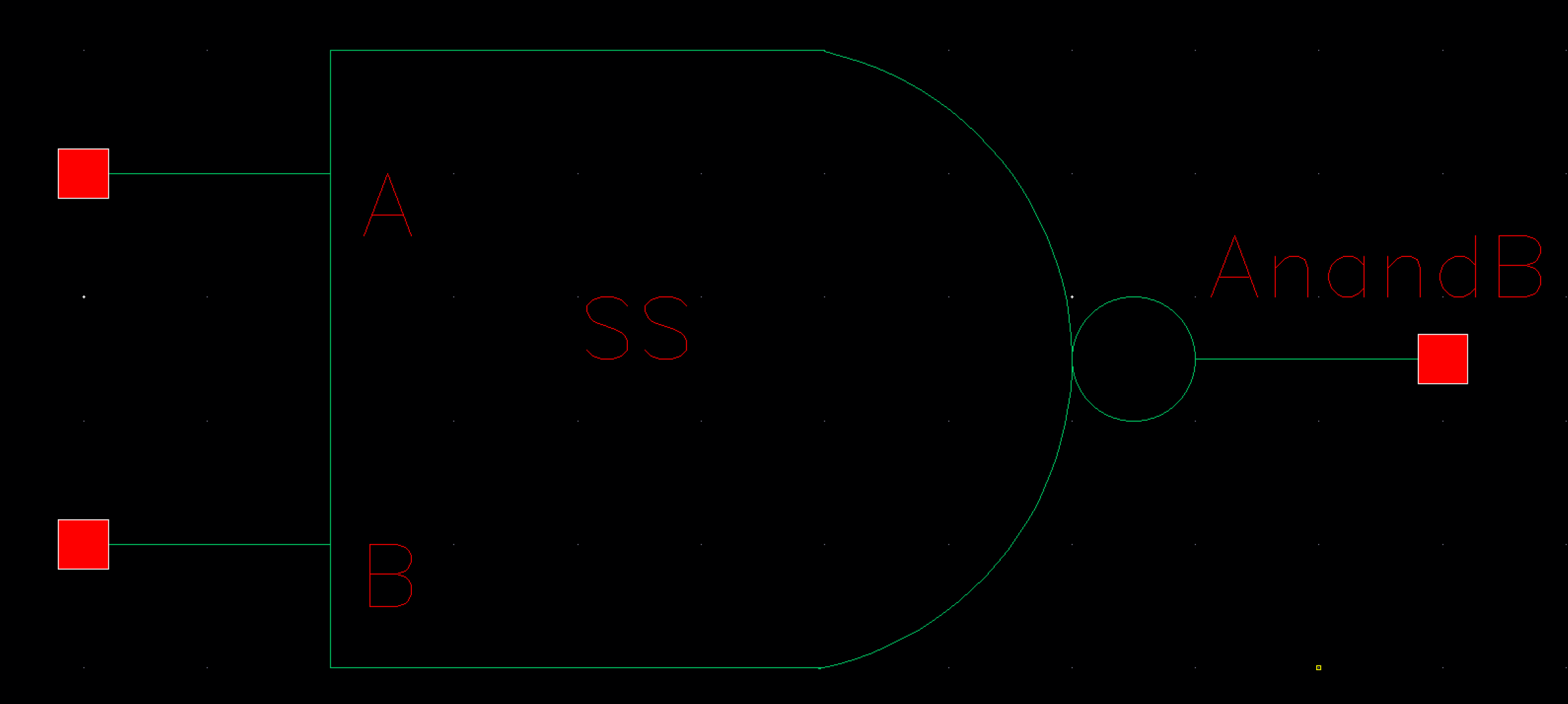
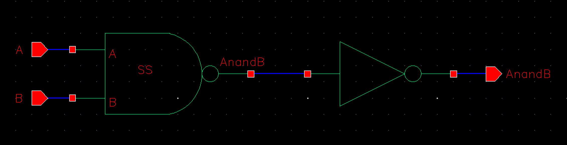
Here is our schematic for our 1-BIT NAND gate and its corresponding symbol...
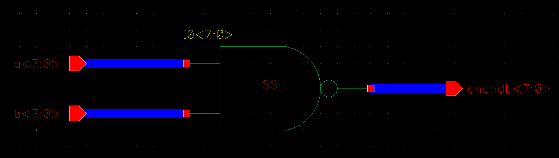
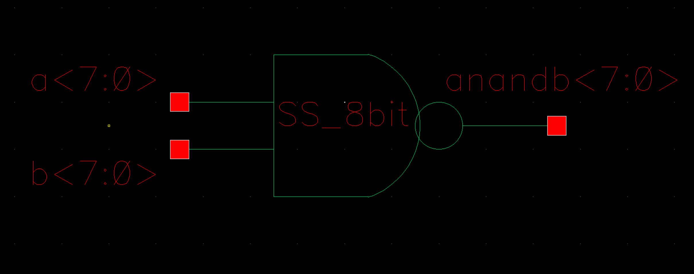
Conversely, we have the 8-BIT NAND gate scheamtic/symbol below with the buses created to carry 8 bits...
Here we have the schematic/symbol for the 1-BIT NOR gate


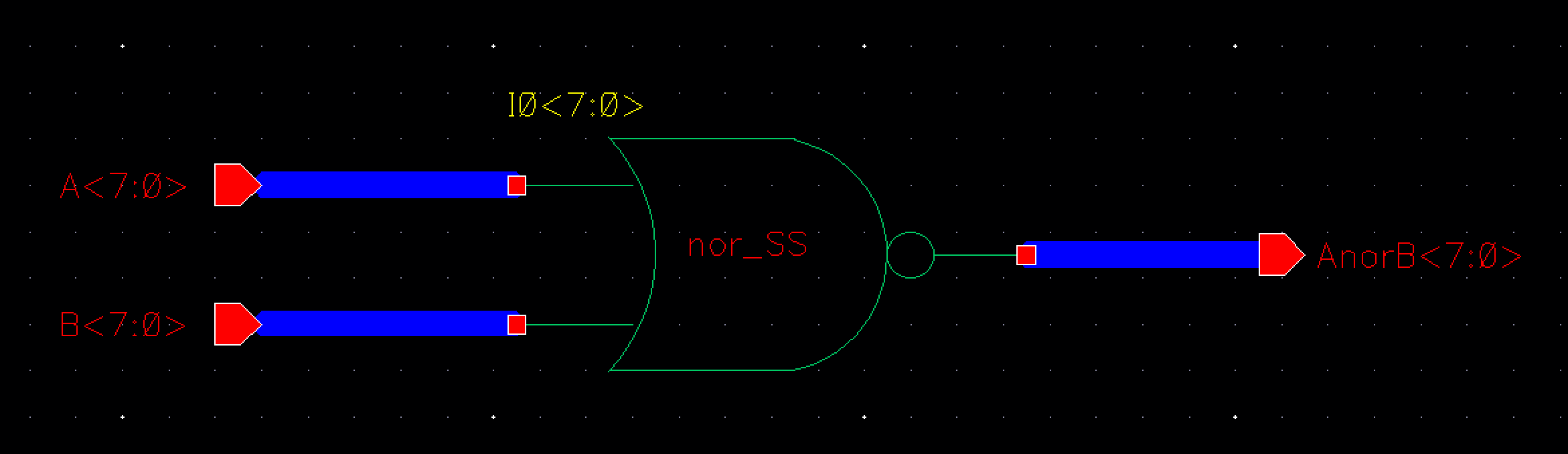
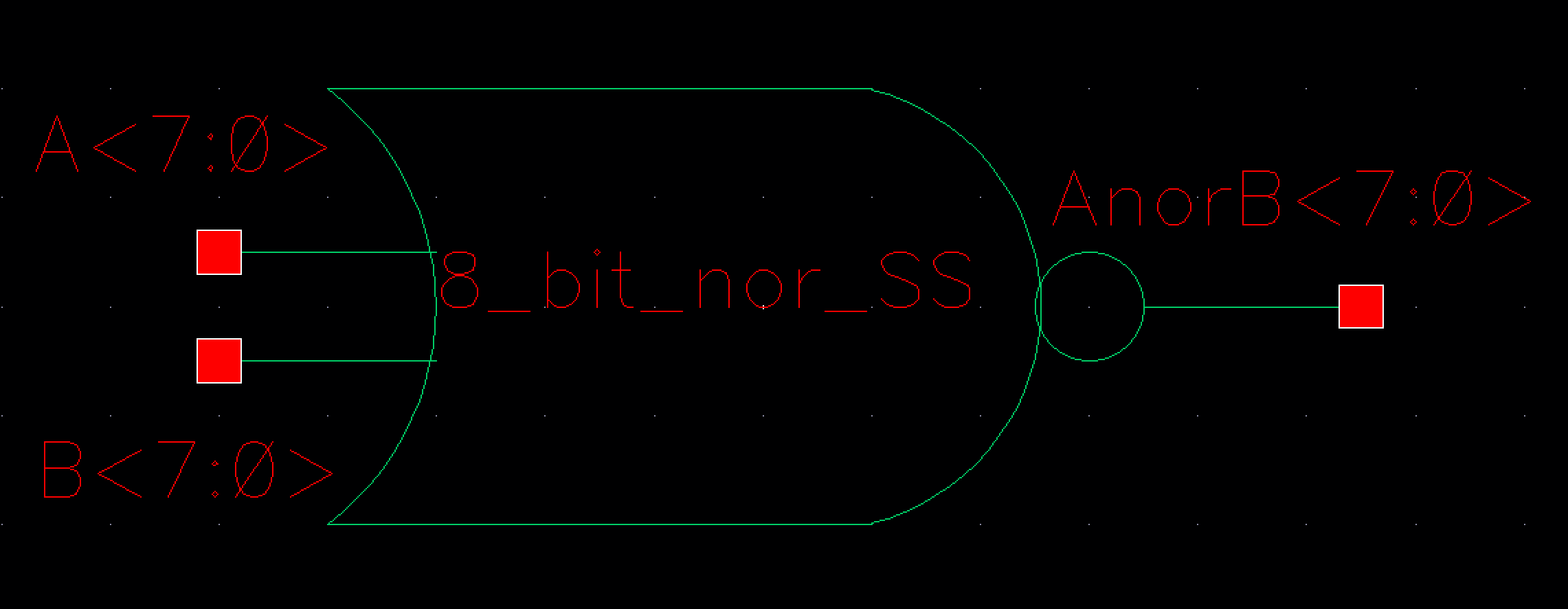
Conversely, here we have the 8-BIT NOR gate schematic/symbol below...
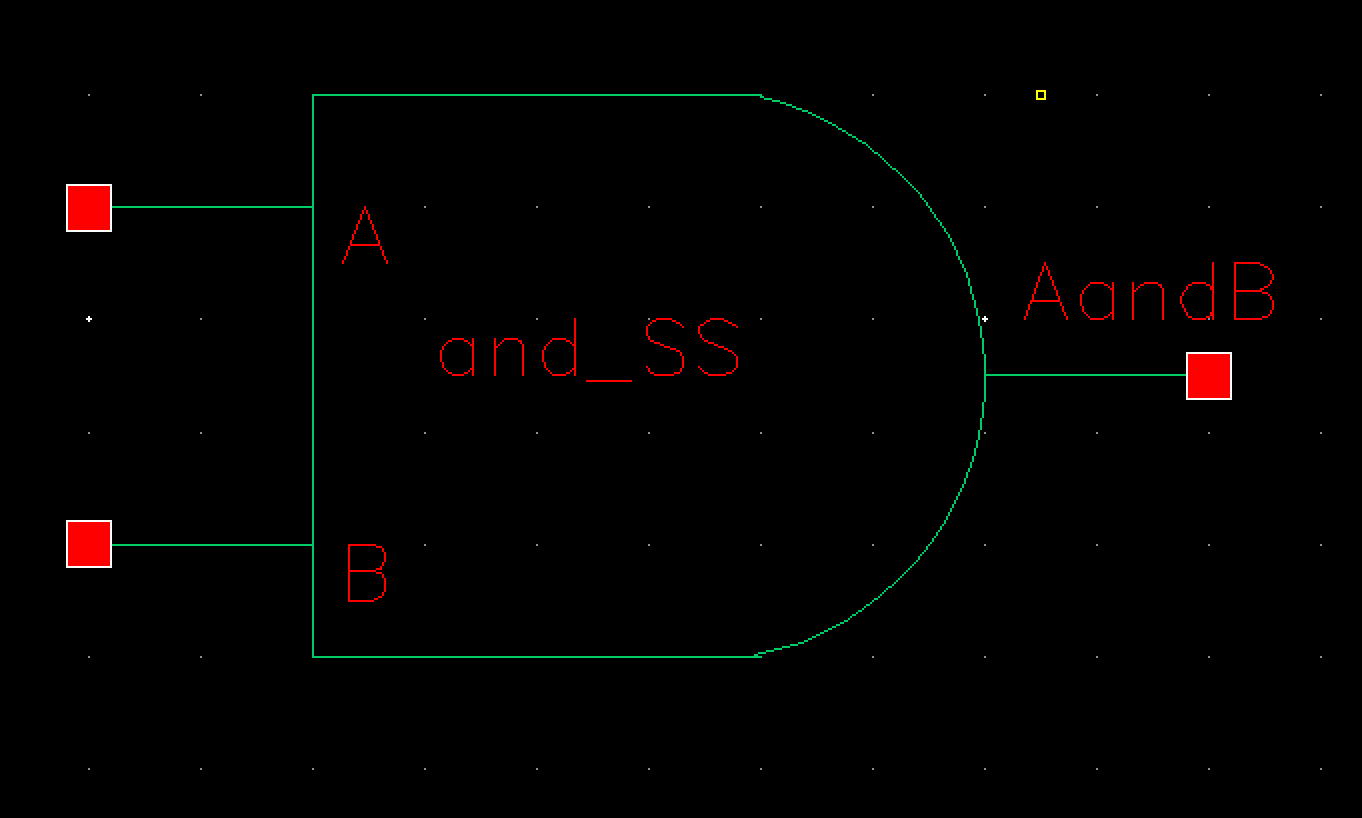
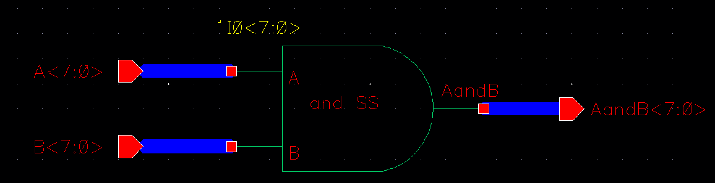
Here we have the schematic/symbol for the 1-BIT AND gate
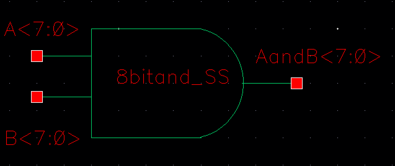
Conversely, here is our schematic/symbol for our 8-BIT AND gate
Here, we have a 1-BIT OR gate schematic/symbol by inverting our original NOR gate...


Here, we have the 8-BIT OR gate with its corresponding schematic/symbol


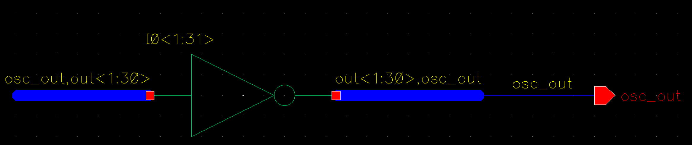
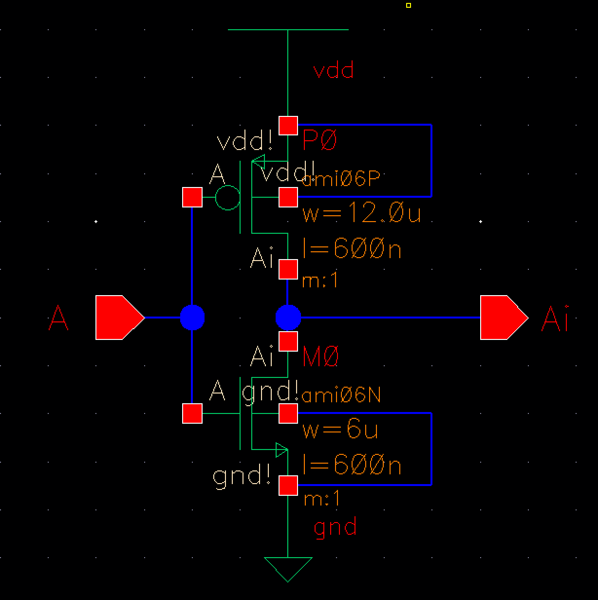
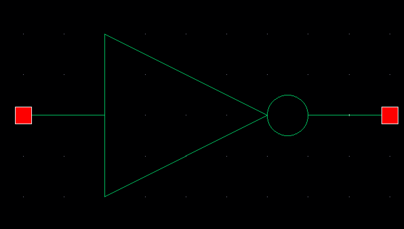
Here, we have a 1-BIT INVERTER with its corresponding schematic/symbol...
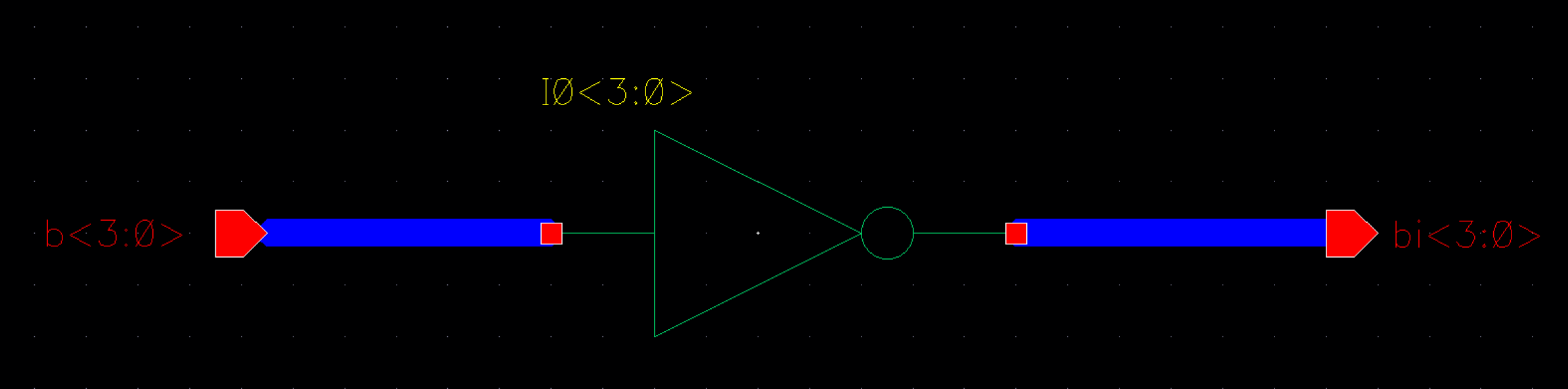
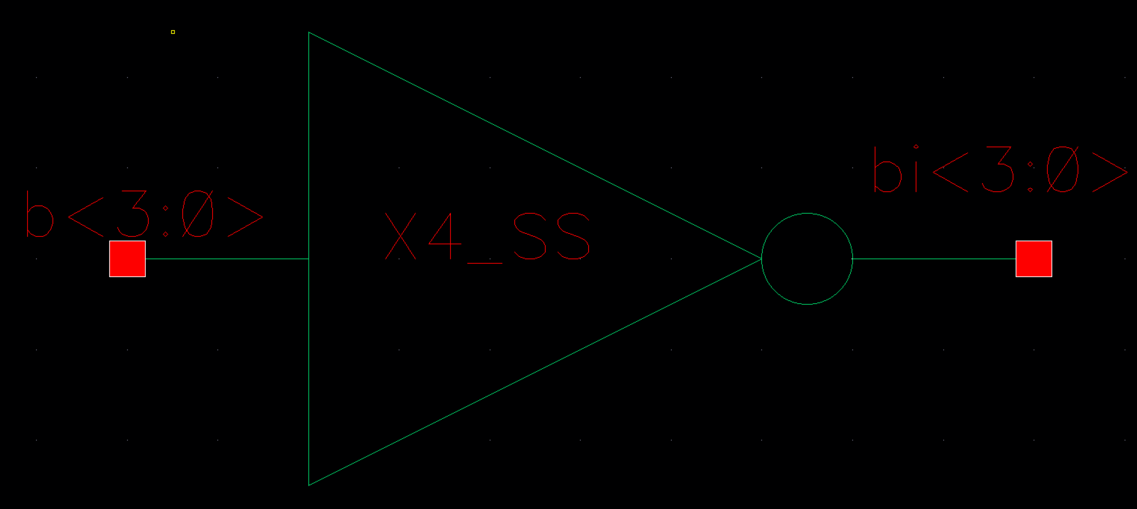
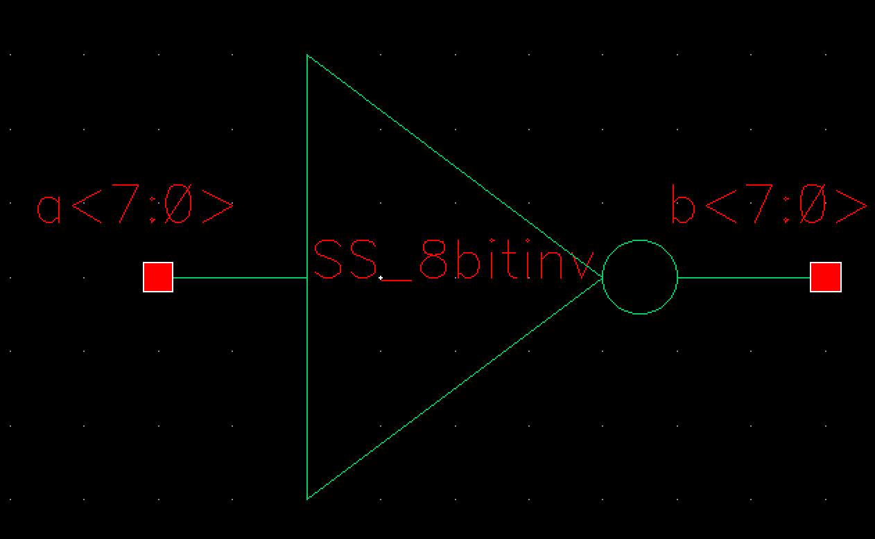
Conversely, we have the 8-BIT INVERTER with its corresponding schematic/symbol...
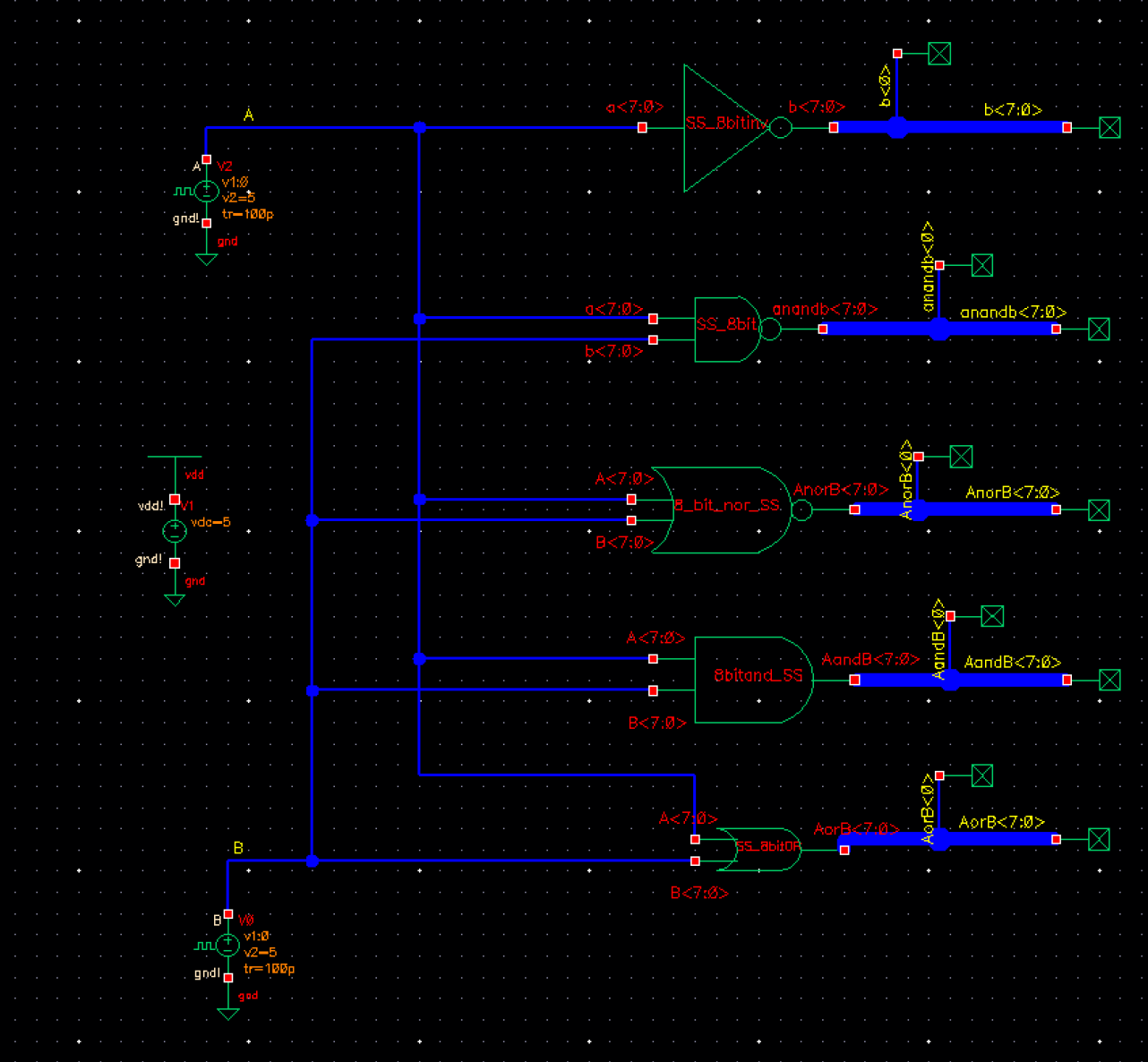
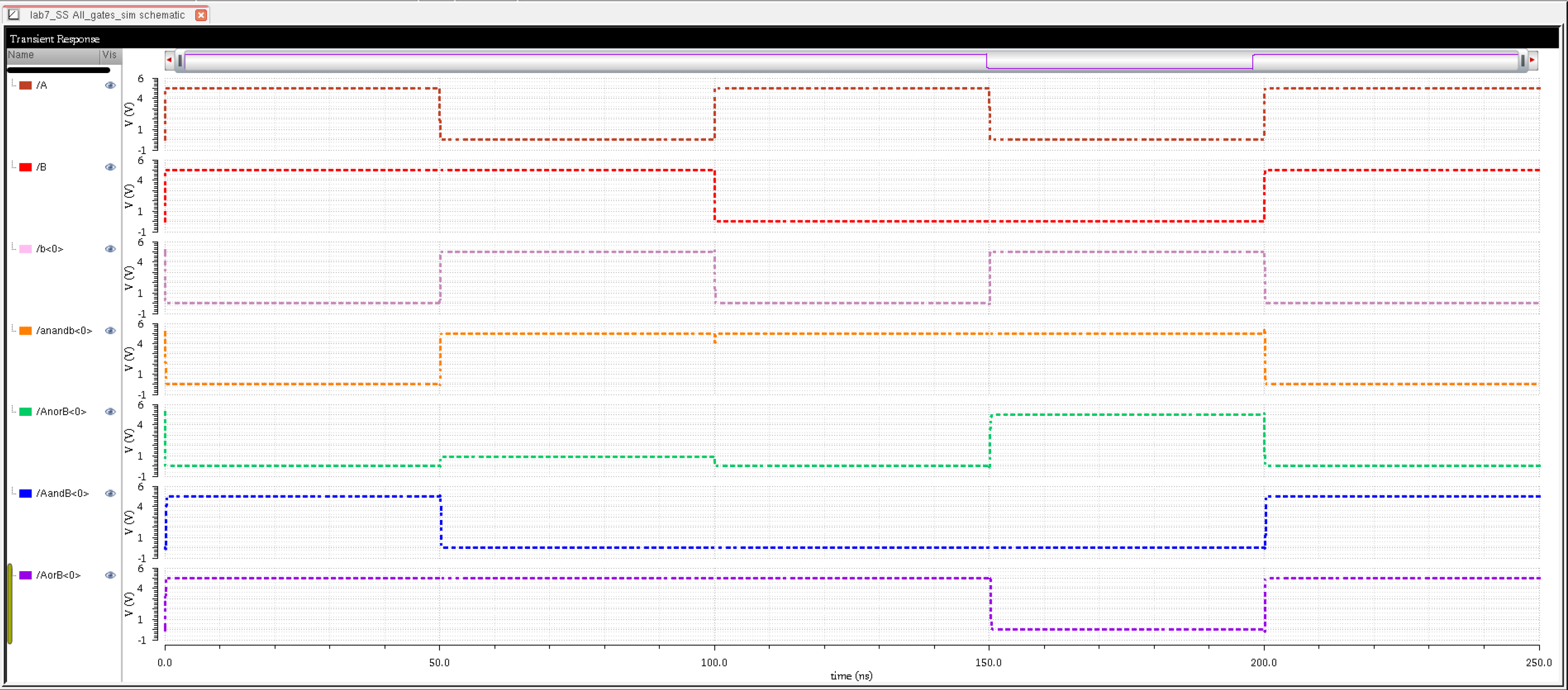
Here, we have the schematic for the simulation of all of the 8-bit gates...
Below, we get the preferred results from our 8-bit gates simulation...
Below,
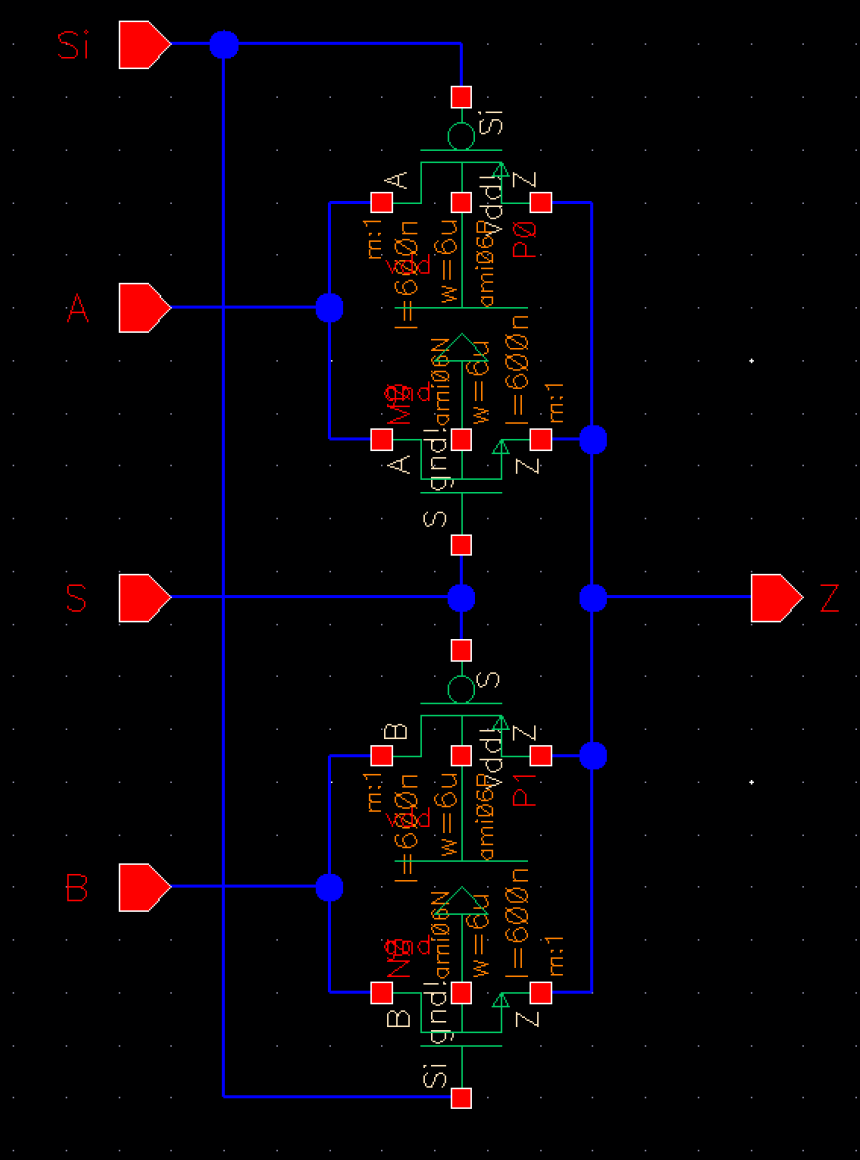
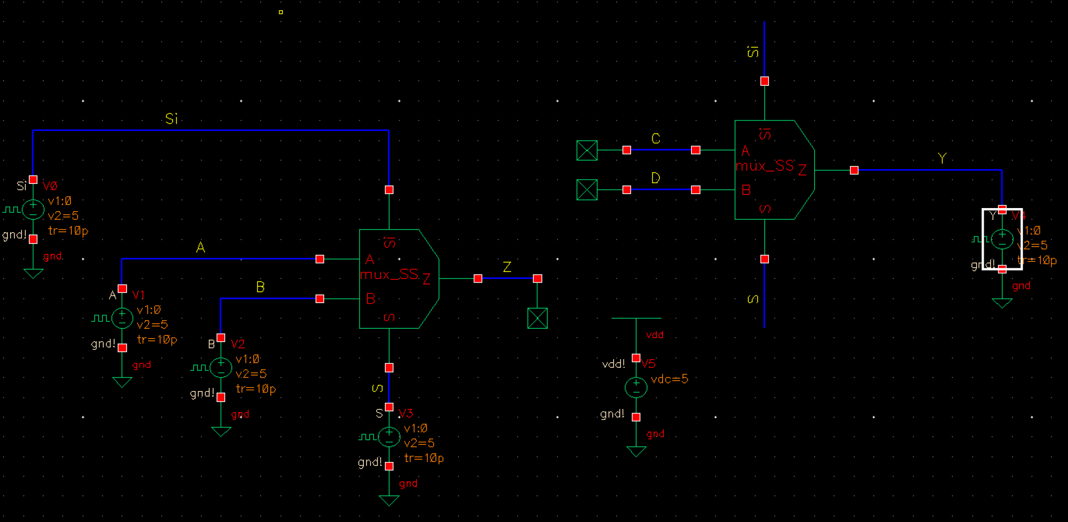
we have the schematic for our MUX... We utilized two transmission gates
which are not on at the same time where Si is simply the inverse of S.
Demuxing, where we utilized S connected to the input of the inverter,
means that the control uses Z as the corresponding input and sends it
to either A or B.
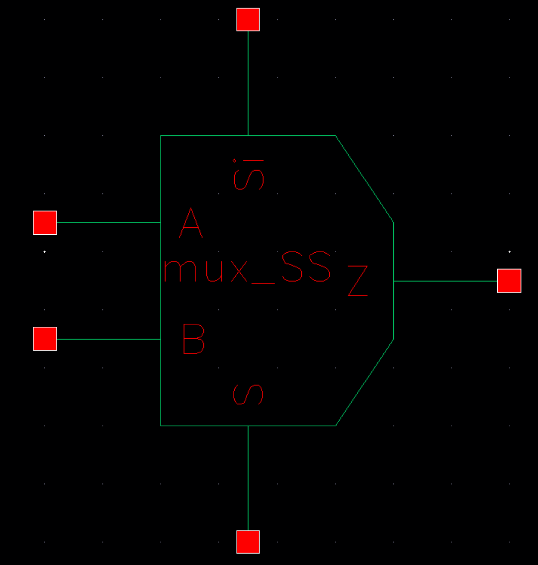
Here is the corresponding symbol for our MUX...
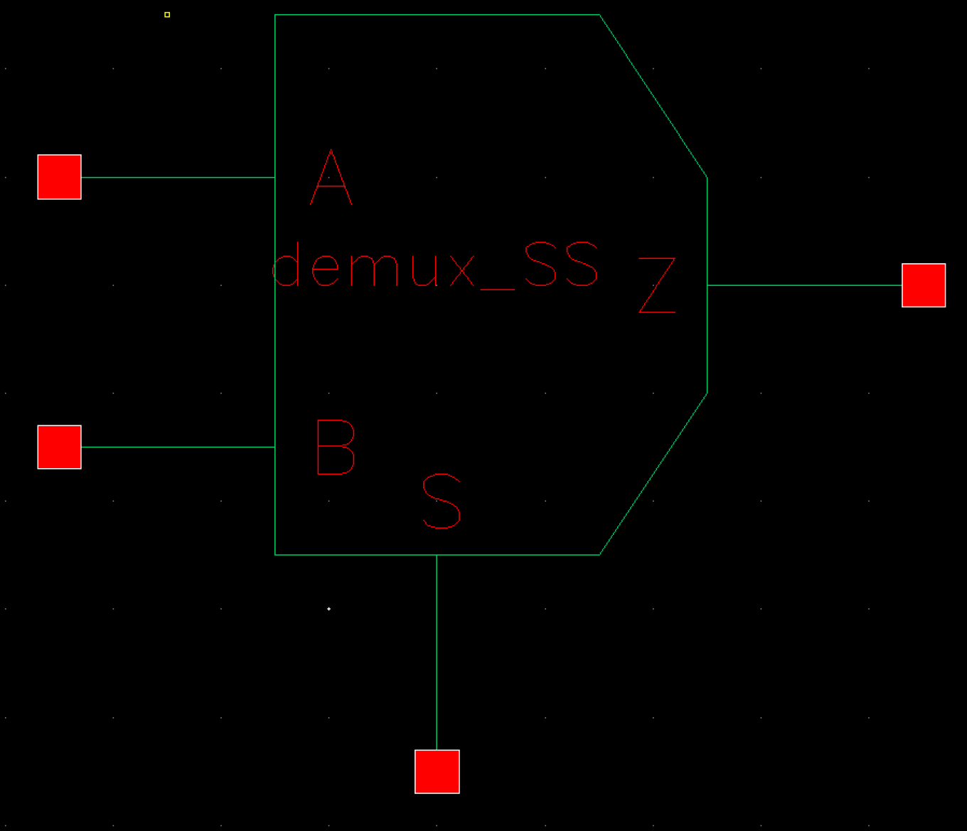
Here is our correspnding DEMUX schematic/symbol...
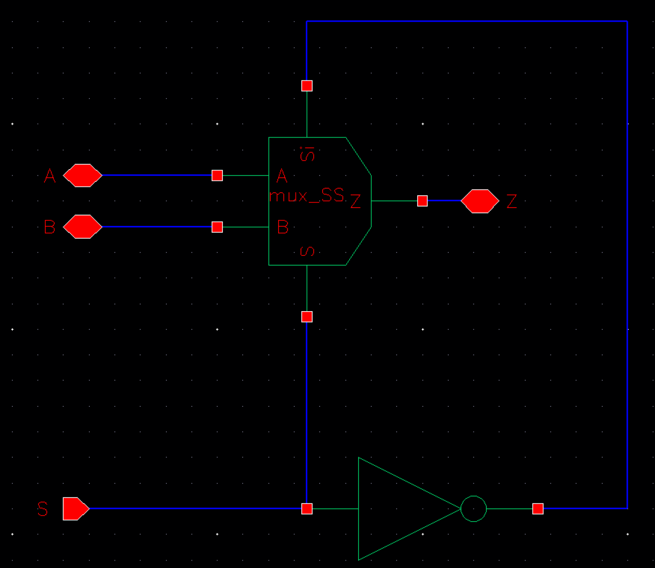
We checked the simulation results of our MUX with the schematic below...
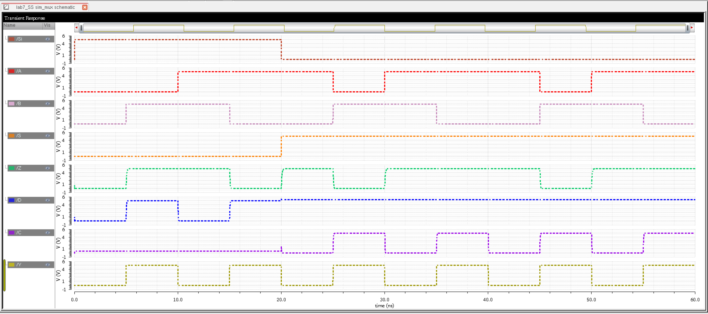
Our simulation results for our MUX came out as expected...
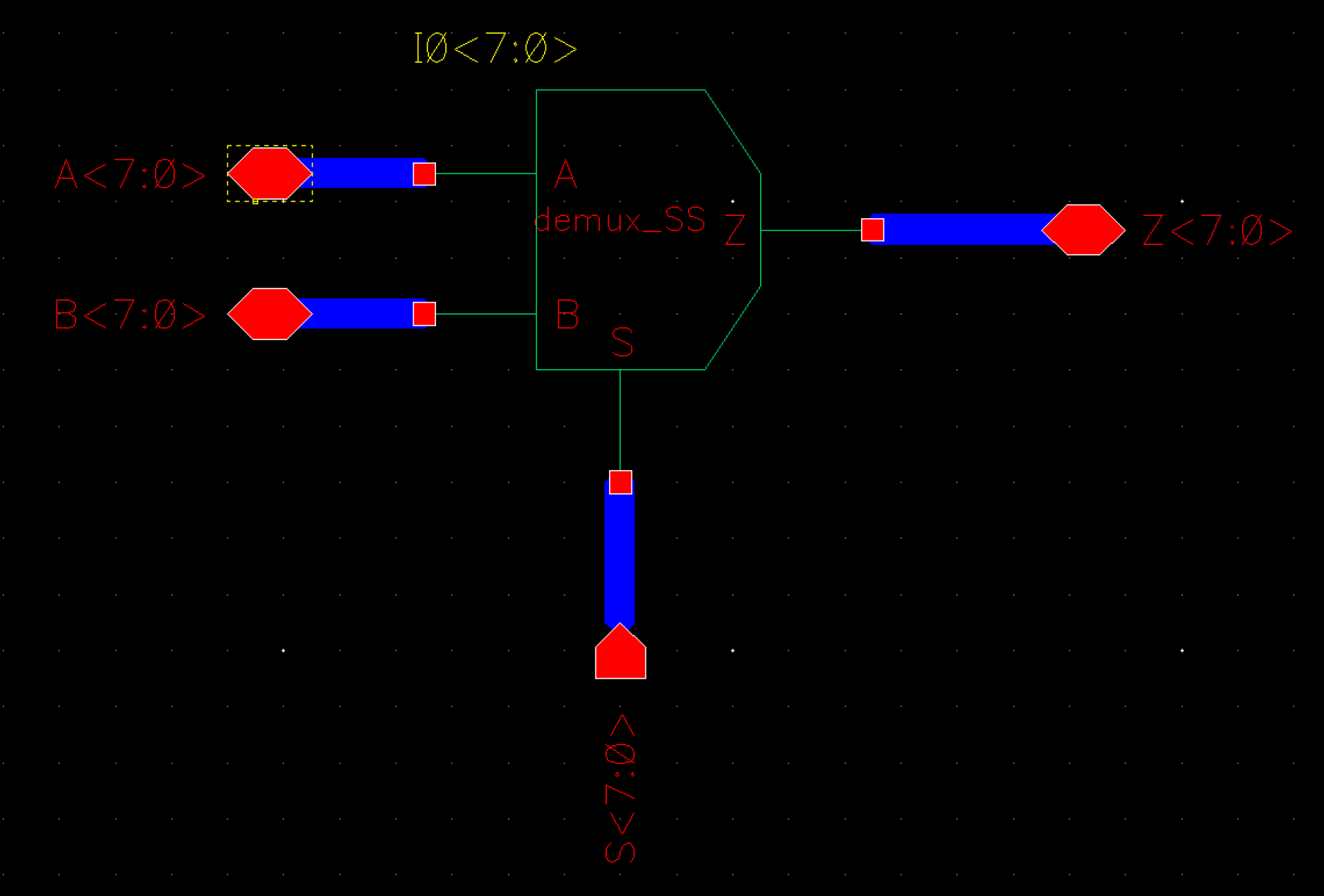
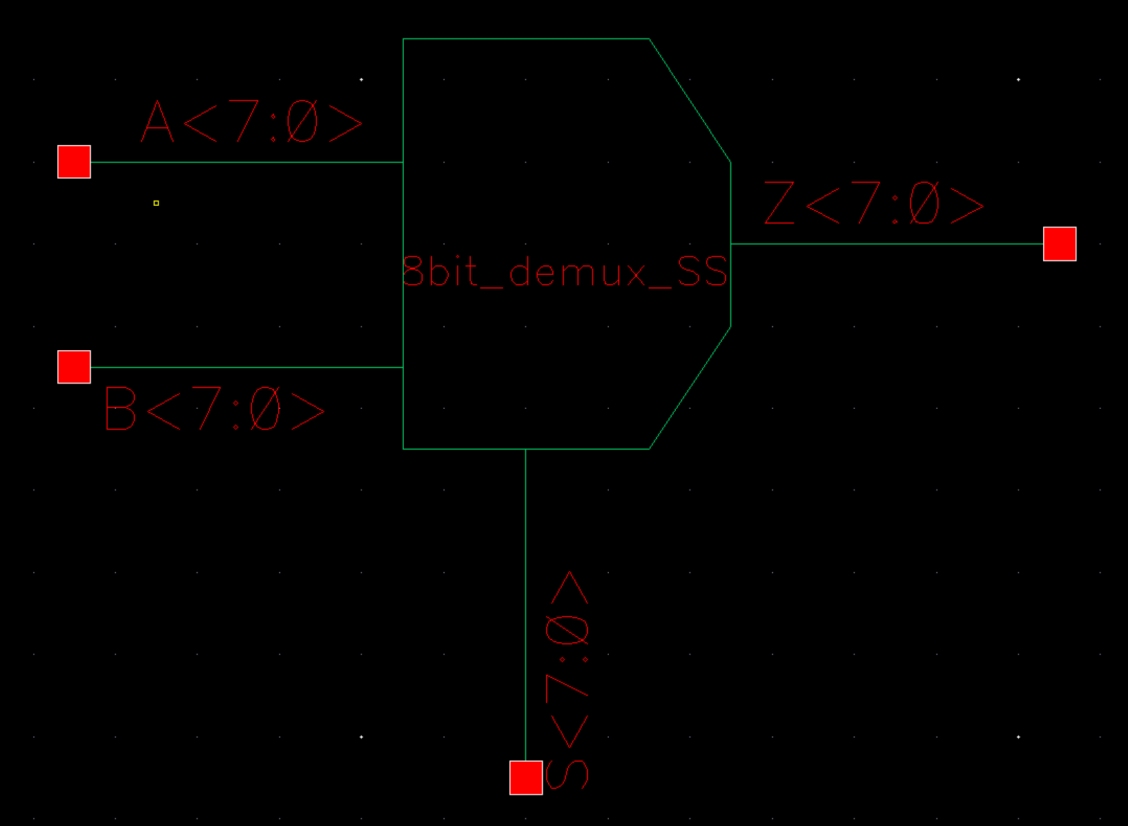
Here, we created the schematic/symbol for an 8-BIT WIDE DEMUX
Below, we can find the schematic for the simulation of our 8-BIT WIDEDEMUX

Below we can find our simulation results for our 8-BIT WIDEDEMUX...

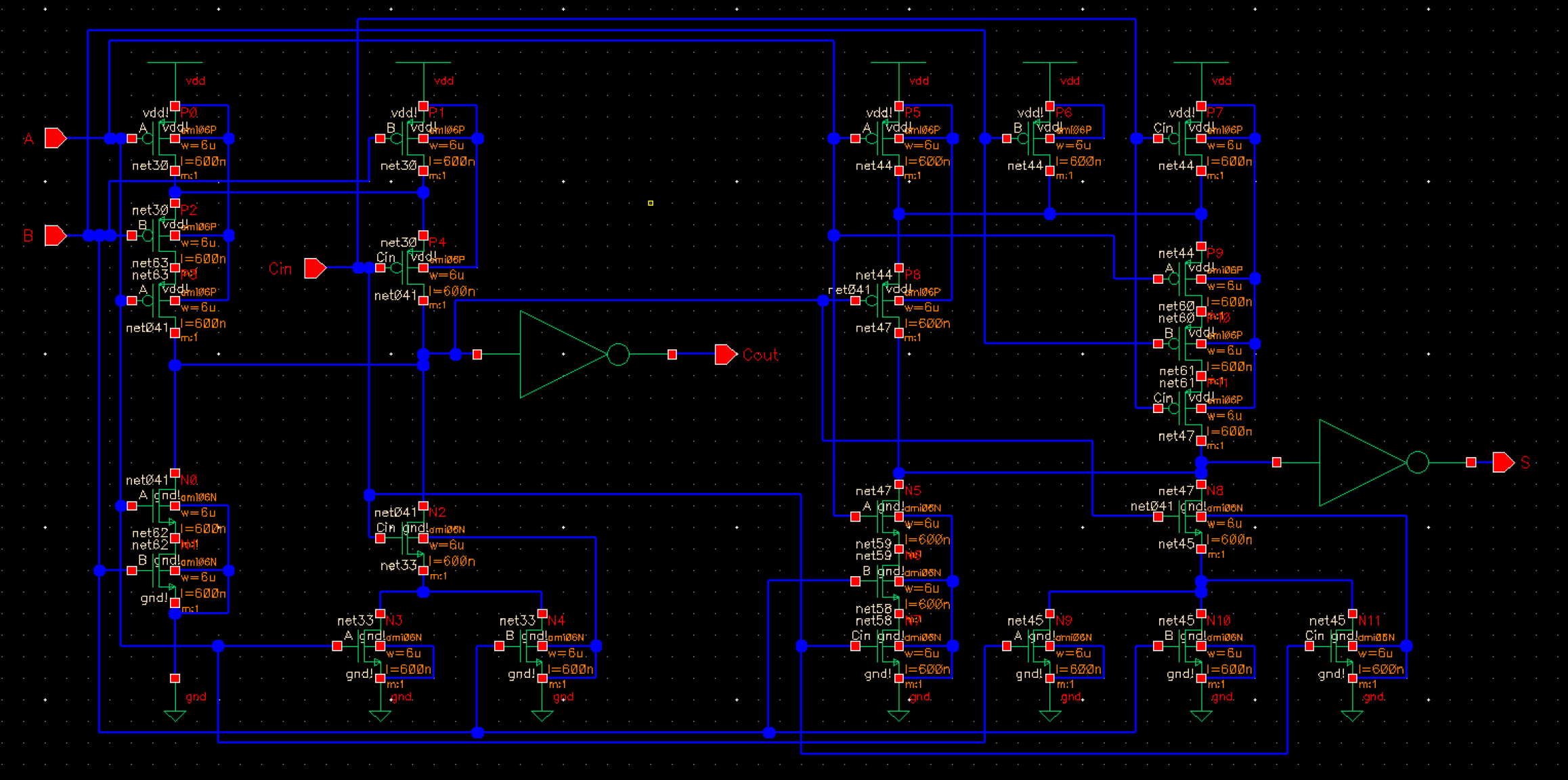
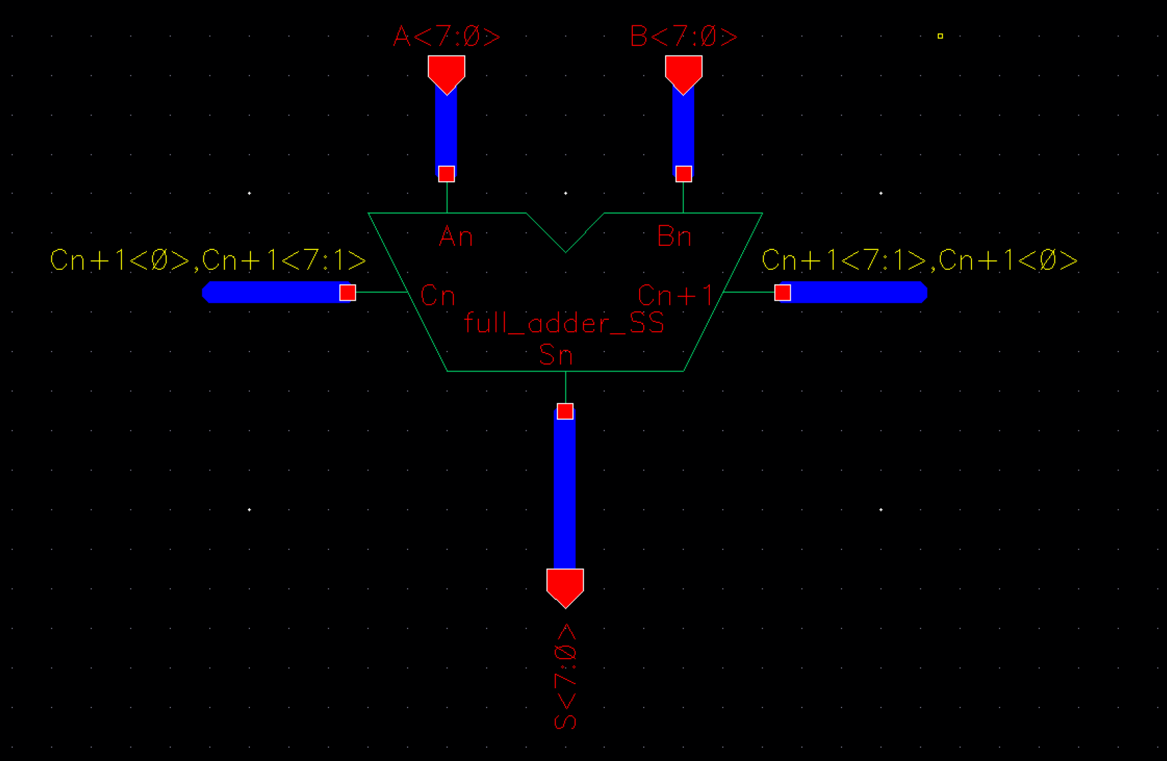
Below, we have the schematic for our AND OR INVERT (AOI) FULL ADDER
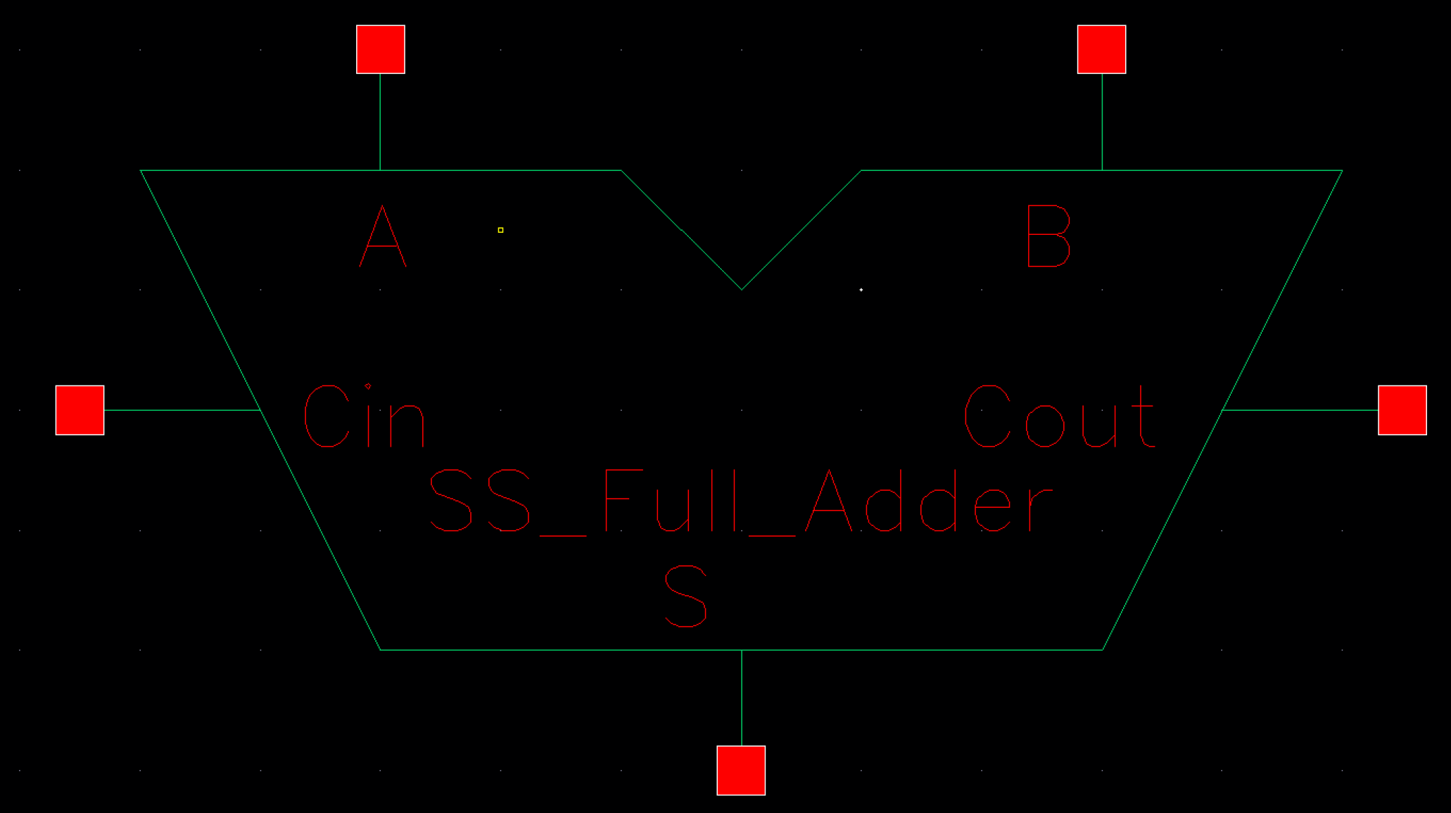
Here is the symbol for our full adder...
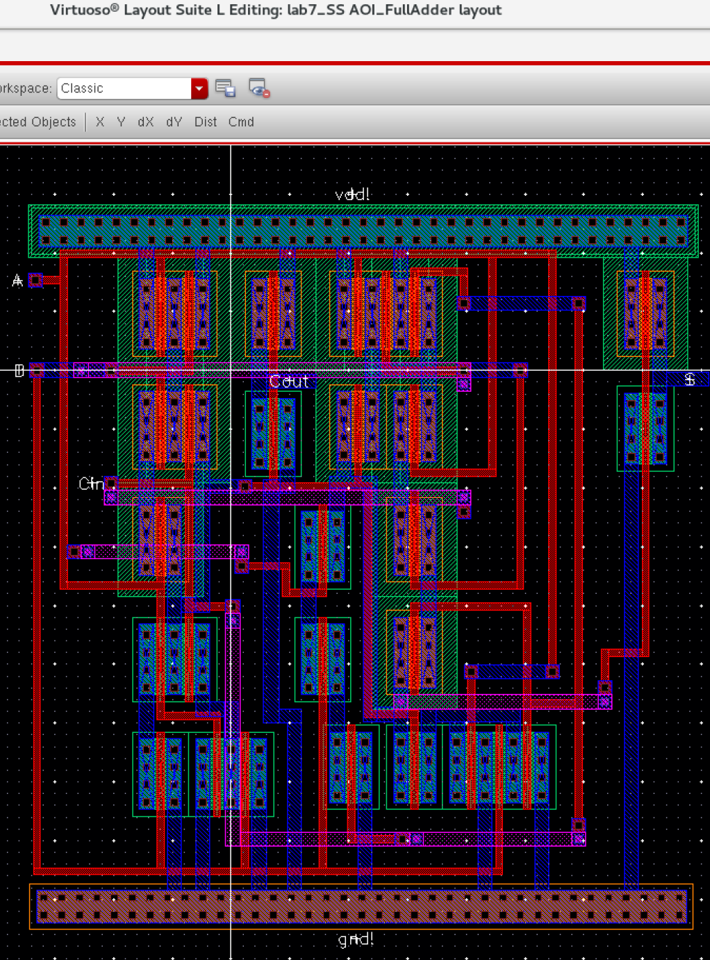
Here is our layout view for our full adder...
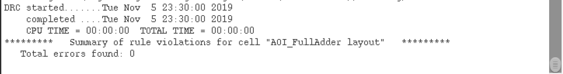
The full adder underwent DRC very nicely...
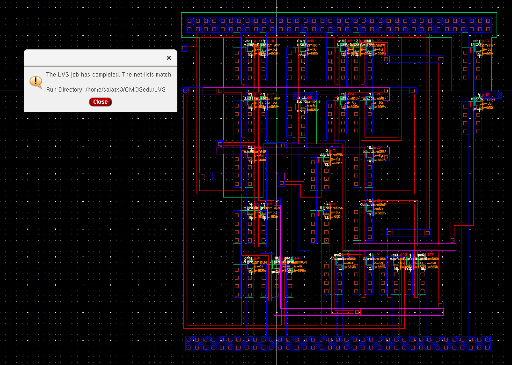
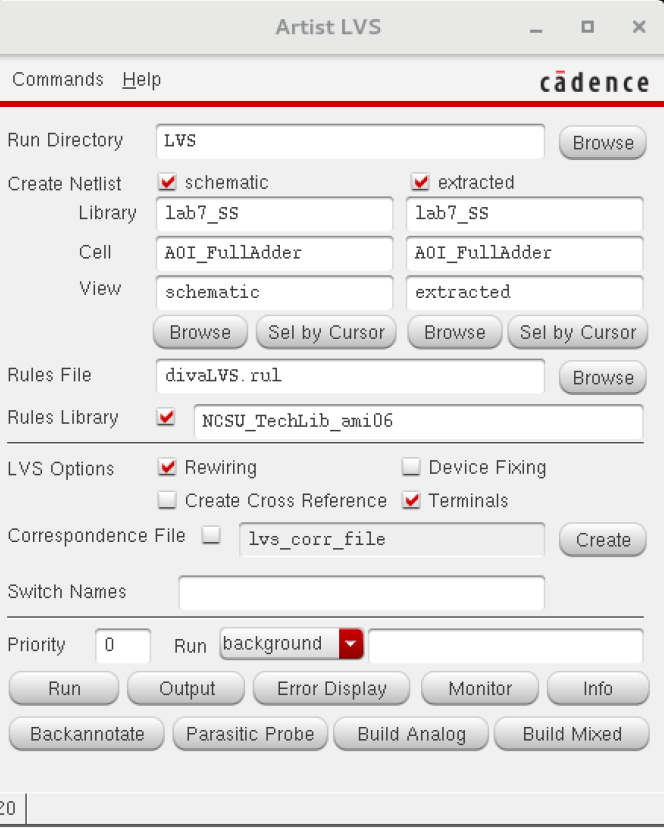
After undergoing LVS, the netlists matched...
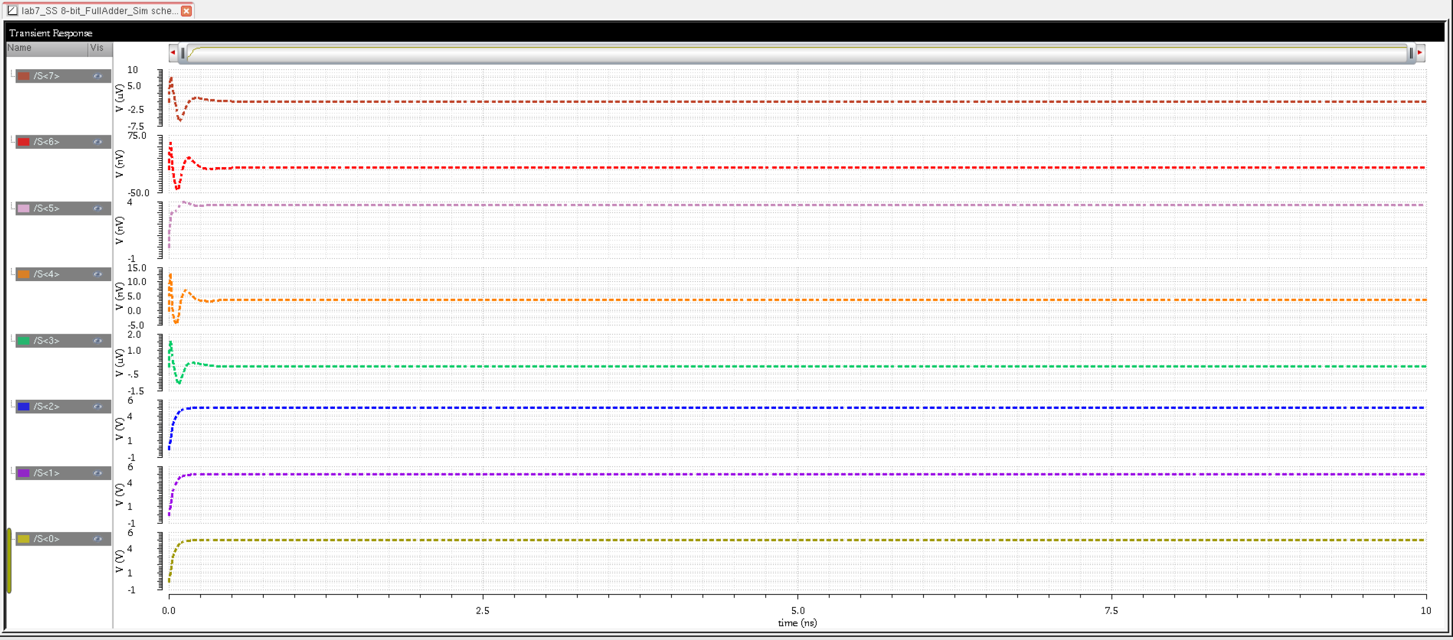
We made sure to create a simulation schematic for our 8-BIT FULL ADDER
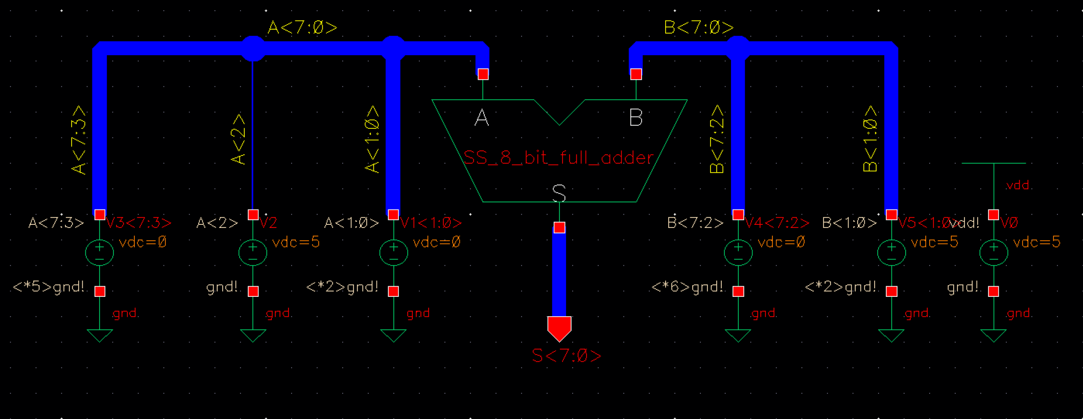
Here
are the corresponding simulation results from allowing A = 00000100 and
B = 00000011 (both in binary) by adjusting the pulse sources
accordingly....
Here is the schematic we used for our 8-BIT FULL ADDER...
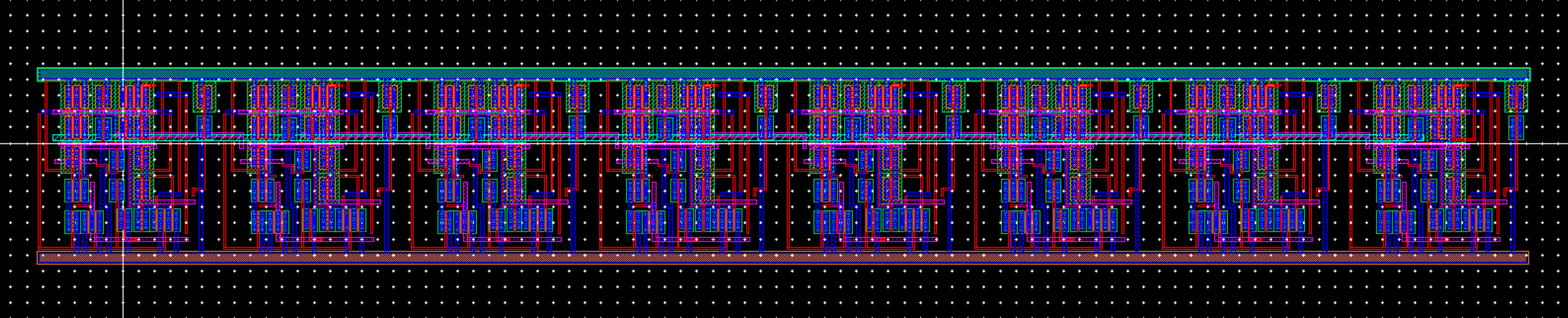
Here, we can see the layout view of our 8-BIT FULL ADDER...
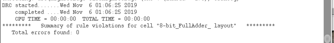
Here, we can see our layout underwent DRC nicely...
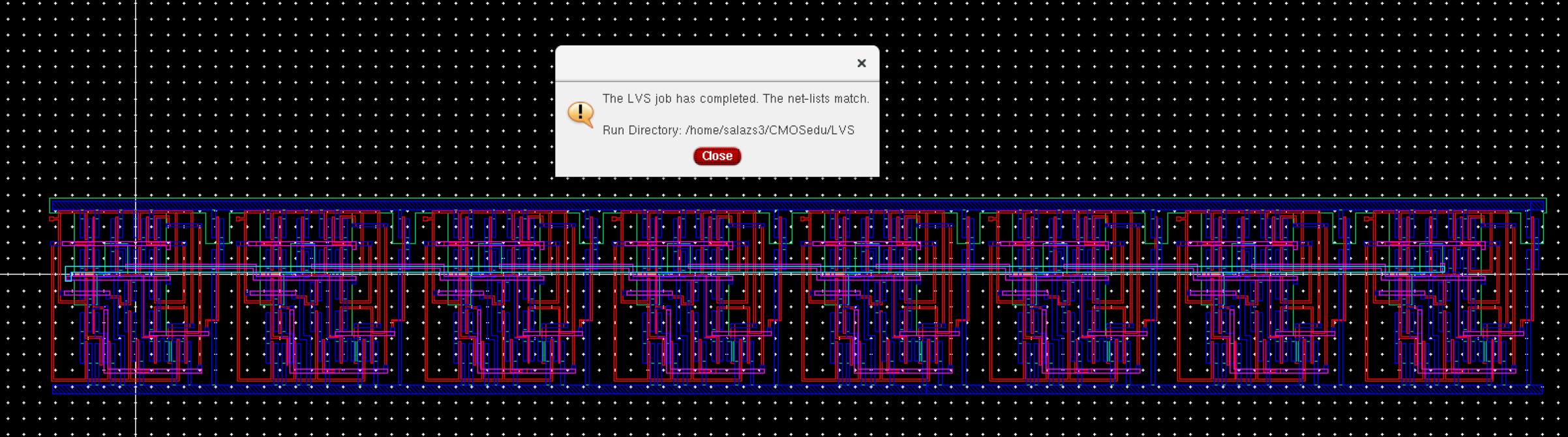
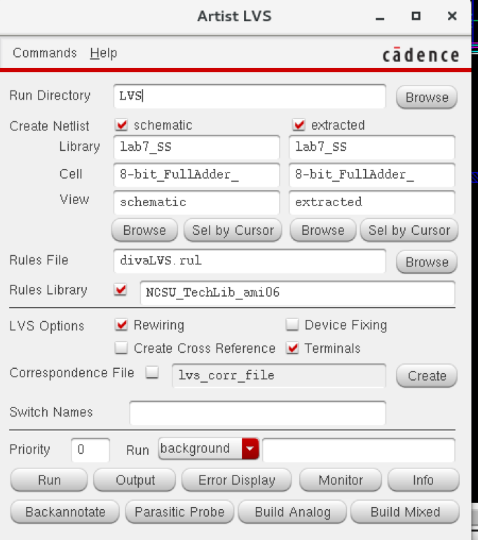
Here, we can see that our 8-BIT FULL ADDER underwent LVS nicely...
As per usual, we made sure to back up our work...
Return to salazs3
Return to EE 421L Labs