Lab 3 - EE 421L
My entire DAC lab 3 files: lab3.zip
We will be working in a layout view in the file called 'Sub_DAC'.
Below is a resistor utilizing the nwell layer to create a rectangle. In order to calculate the proper length of the nwell given the minimum width of 3.6 microns in the C5 process, we utilize the equation below.
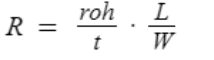
Given the sheet metal resistance term in the equation 'roh/t' is approximately ohms, we can calculate our length given a 10-k resistance and choosing 6 microns as our width (in order to not violate the rule where the values are not whole numbers when dividing by 0.15).
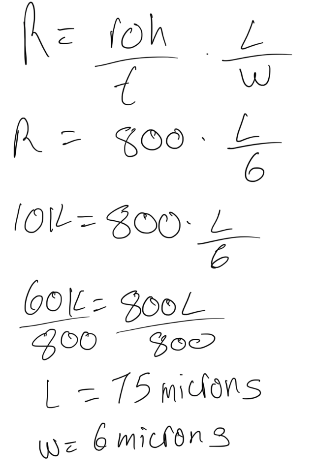
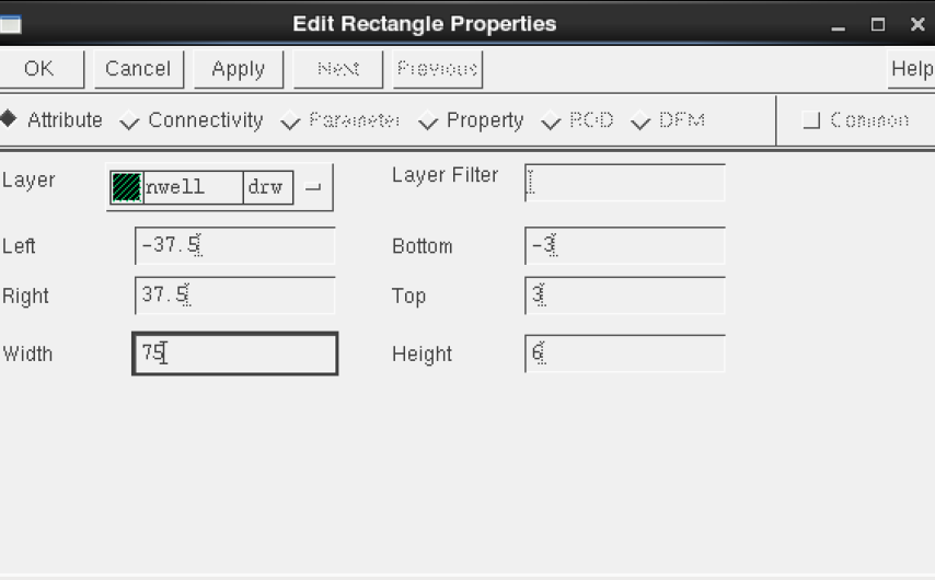
Length = 75 microns, Width = 6 microns
Below, we can see our selected rectangle dimensions are properly selected in the rectangle properties for our nwell layout.
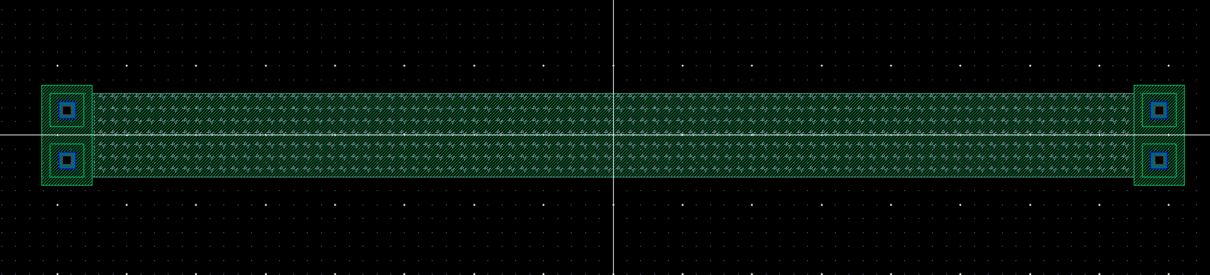
This is the resistor with the 2 rows of ntap objects snapped to both respective sides of the nwell (found under the NCSU_Techlib_ami06" library and instantiated into my layout view).
This is our resistor already properly defined utilizing the res_id layer placed on top of the n-well.
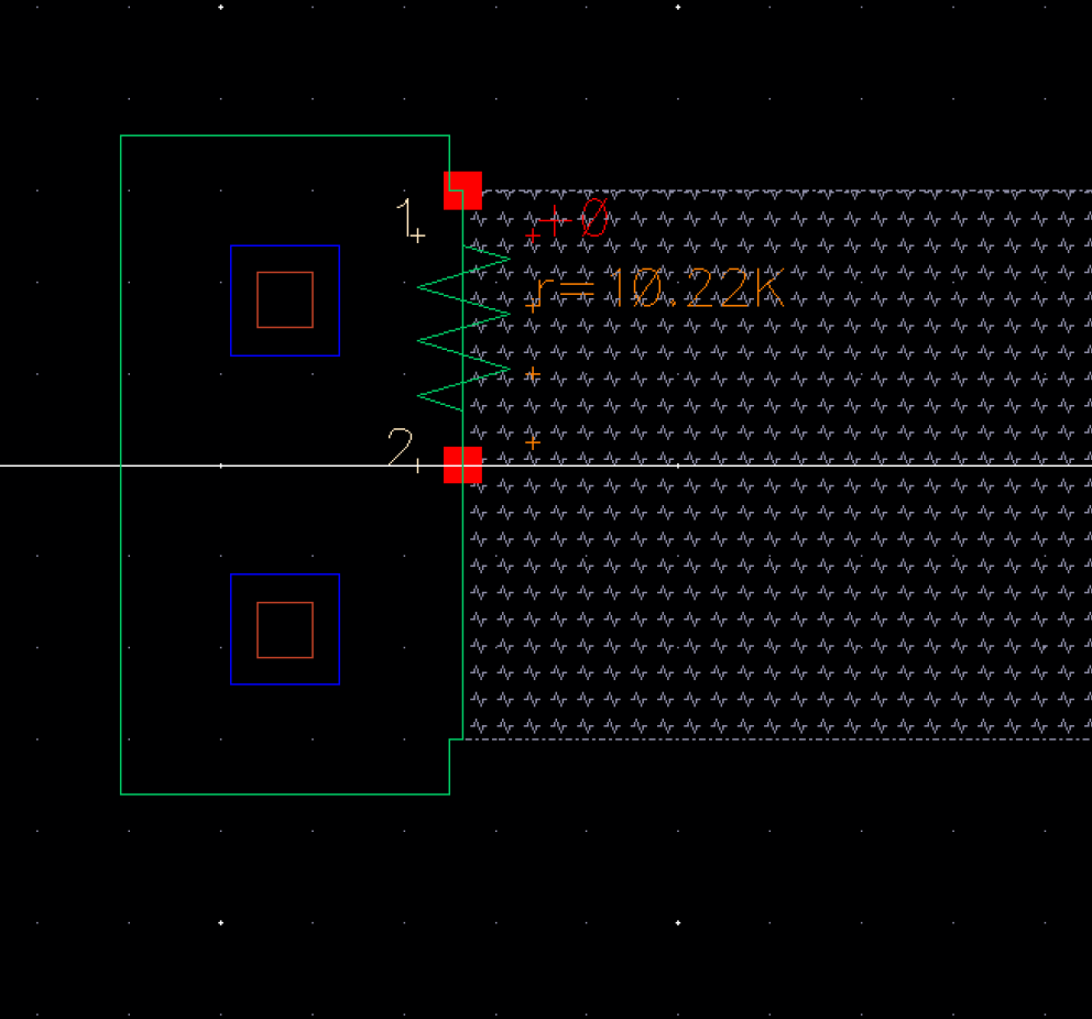
This is the overall extracted view of our resistor.
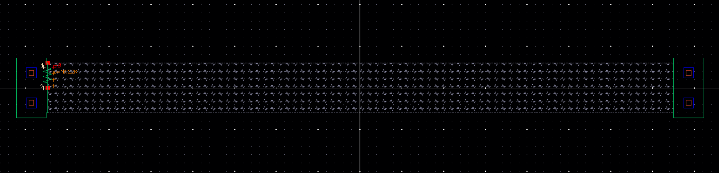
This is the zoomed-in view of our extracted resistor. As we can see, our resistor is approximately 10k ohms.
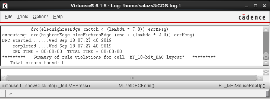
The layout of our resistor successfully undergoes DRC.
The
next step was to create a schematic of a single DAC bit section. This
made up my 'Sub_DAC' layout file. An LVS and a DRC were successfully
checked.
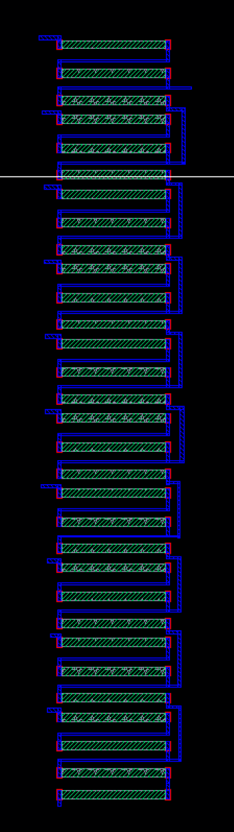
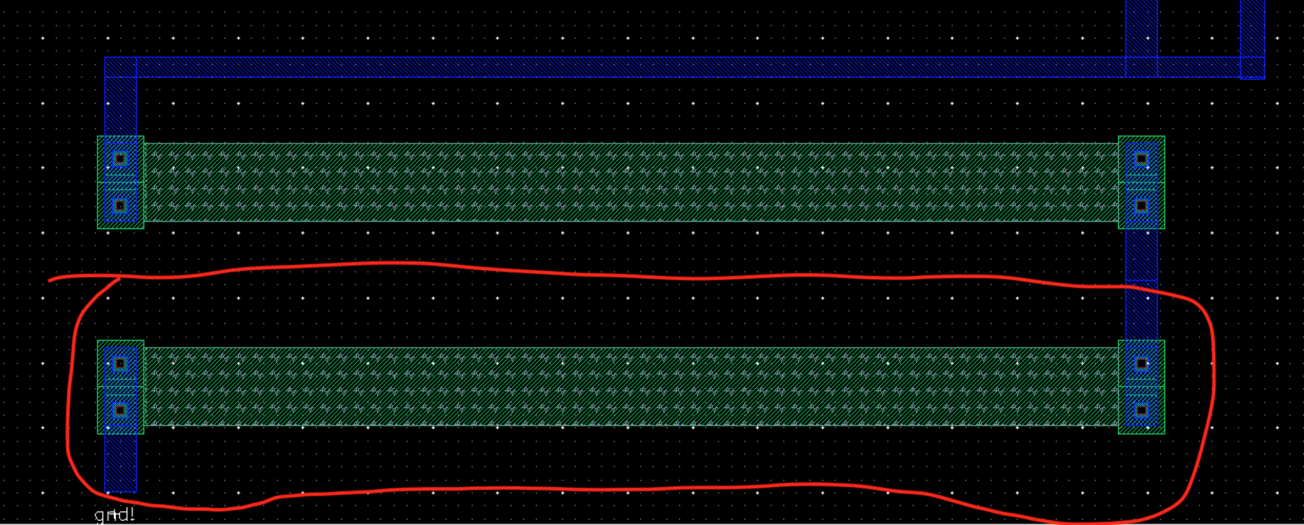
We made sure to remove any pin names on my 'Sub_DAC' layout in order to avoid conflicts in the netlists matching. After instantiating my 'Sub_DAC' layout ten times in a column, I made sure to add corresponding B[9:0] pins and the 'Vout' pin as well.
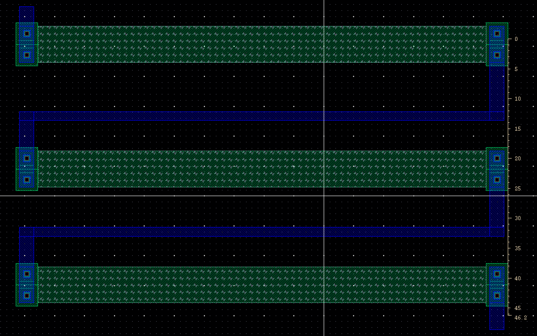
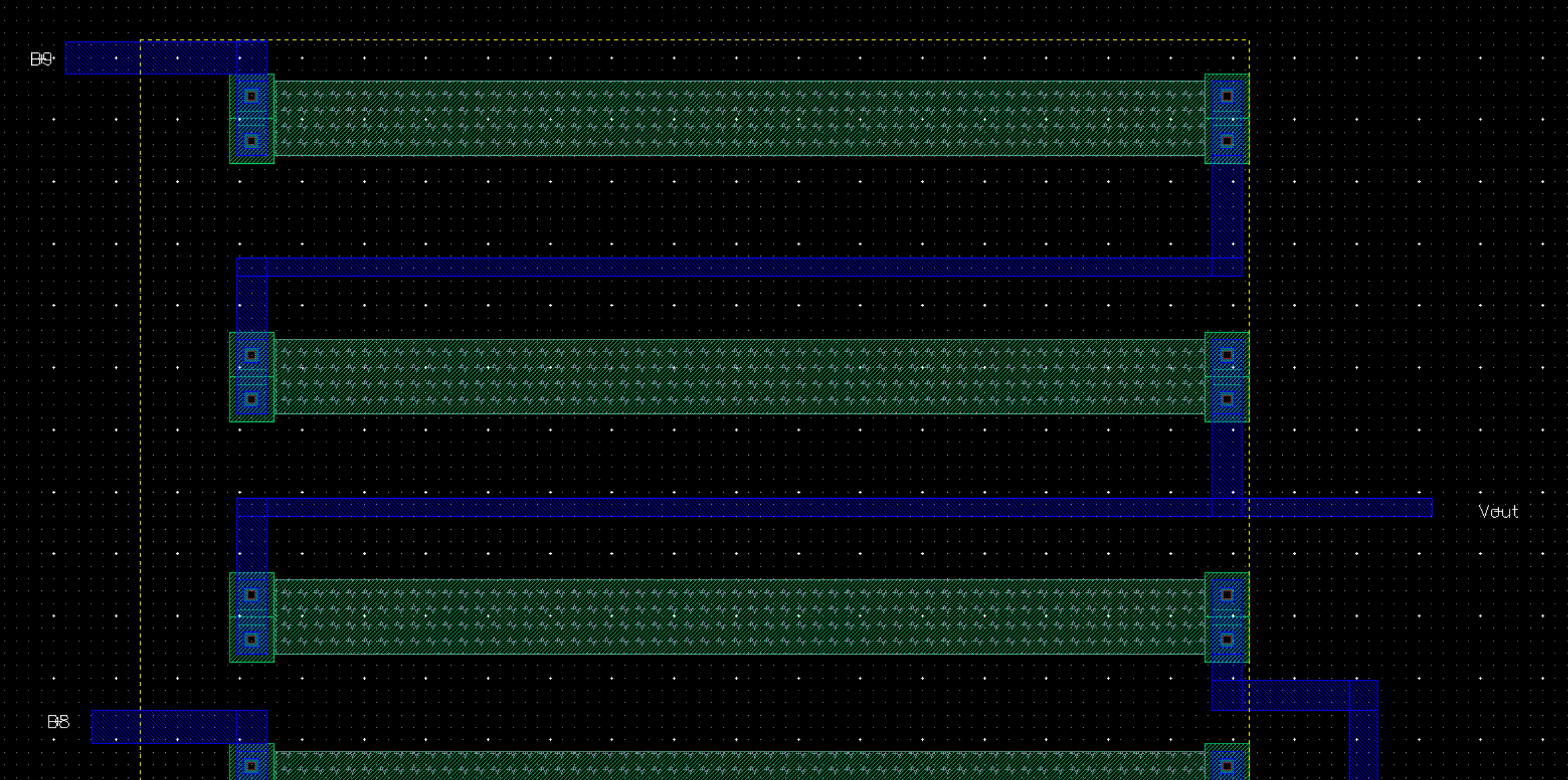
This is zoomed in portion of my 'Entire_DAC' layout file that highlights the B[9] and Vout pins, respectively.
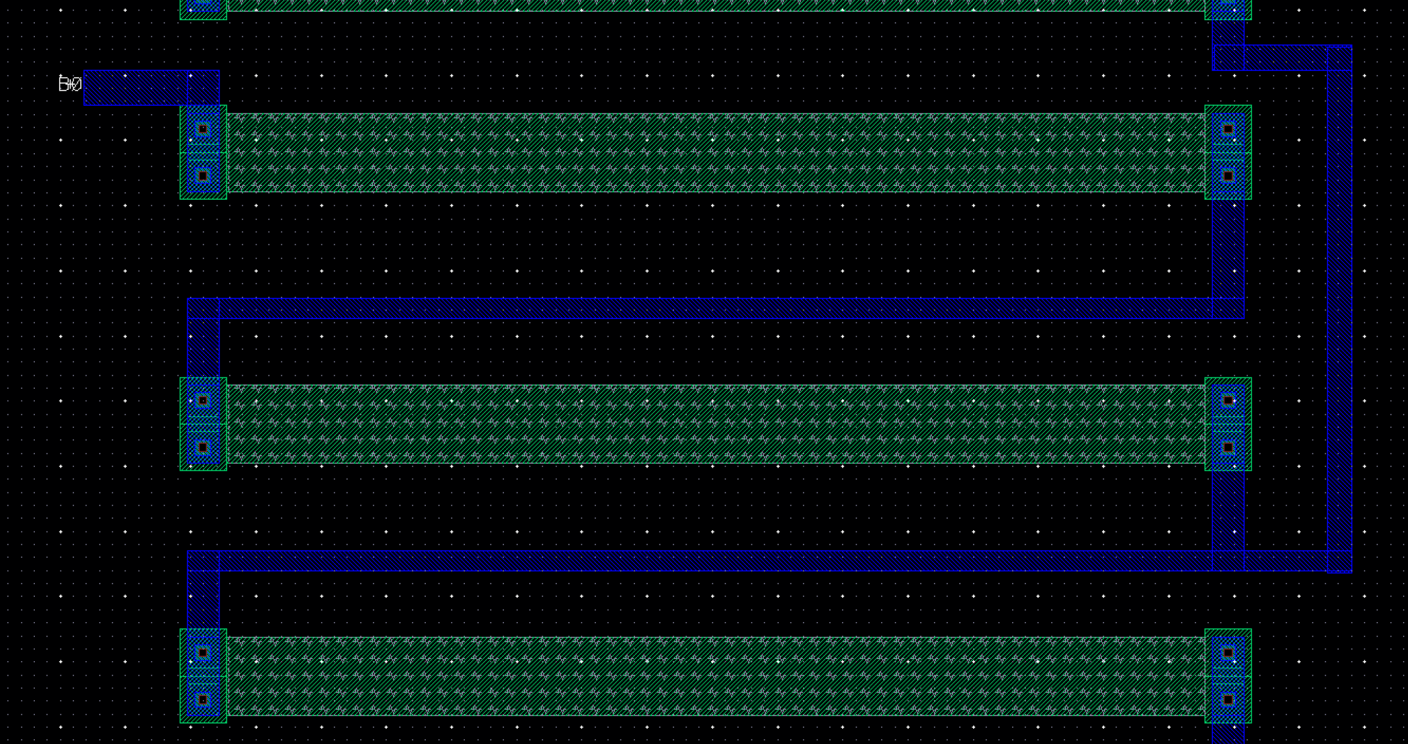
This view highlights the B[0] of our 'Entire_DAC' layout.
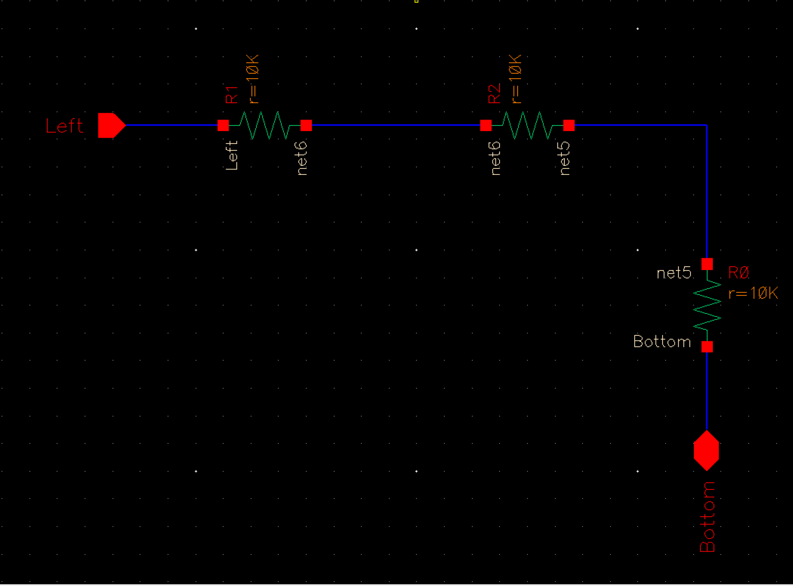
With further inspection, we can see I added a single 10-k resistor at the bottom of my 'Entire_DAC' layout in order to LVS correctly.
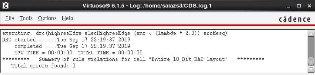
This verfies my 'Entire_DAC' layout undergoes DRC with no errors.
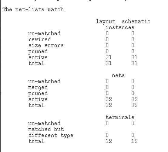
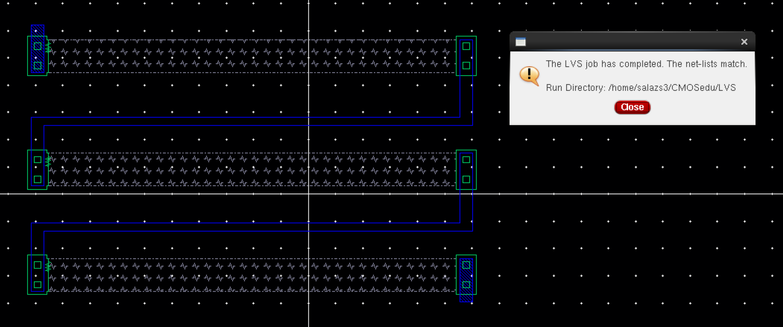
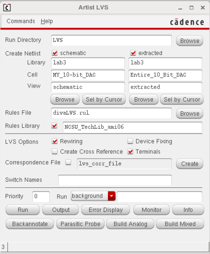
LVS also completes with no errors, and the net-lists match...
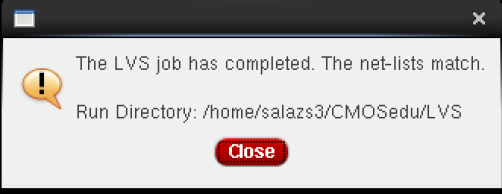
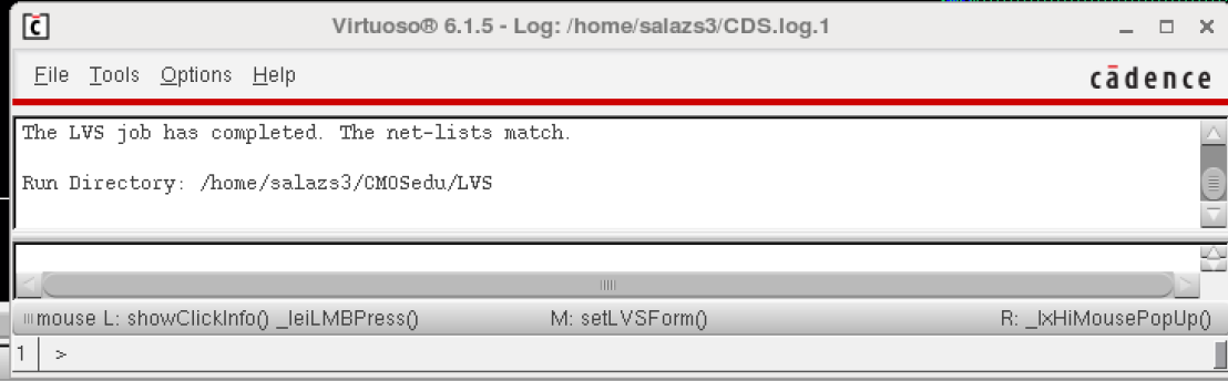
This is the output window after completing LVS