Lab 2 - EE 421L
Design of a 10-bit digital-to-analog converter (DAC)
Authored by: Steve Salazar-Rivas
salazs3@unlv.nevada.edu
September 11, 2019
PRELAB:
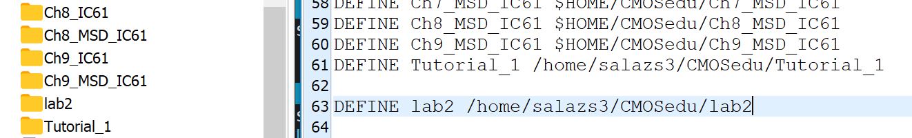
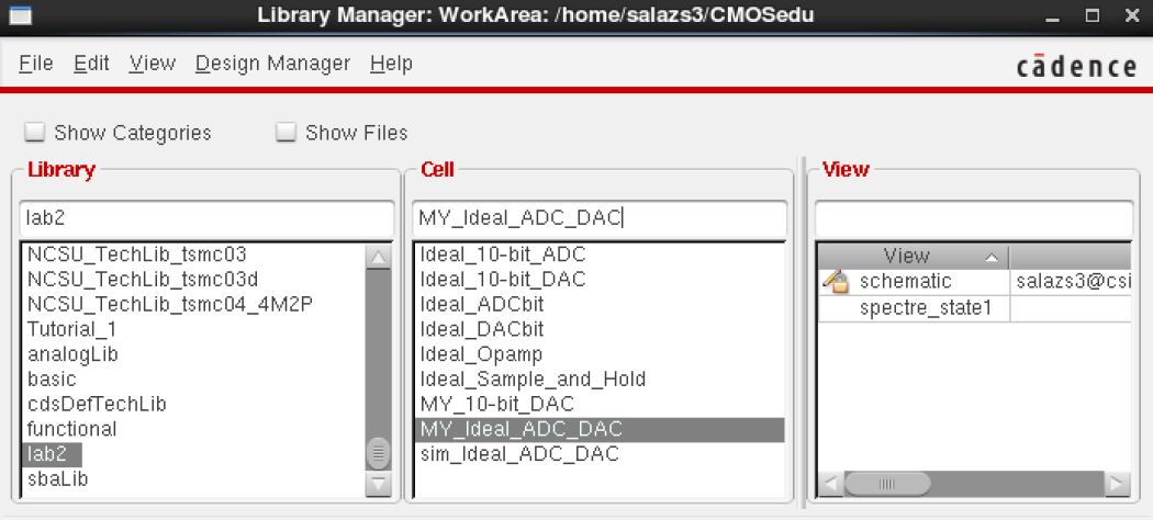
To
begin, I downloaded the lab2.zip file to my desktop. Concurrently, I
uploaded this file to my design directory of CMOSedu. After, I made
sure to add a line in my cds.lib file defining a new library for
our new zip file. Below, we can verify these steps were done correctly
by looking at my Library Manager and my cds.lib file.
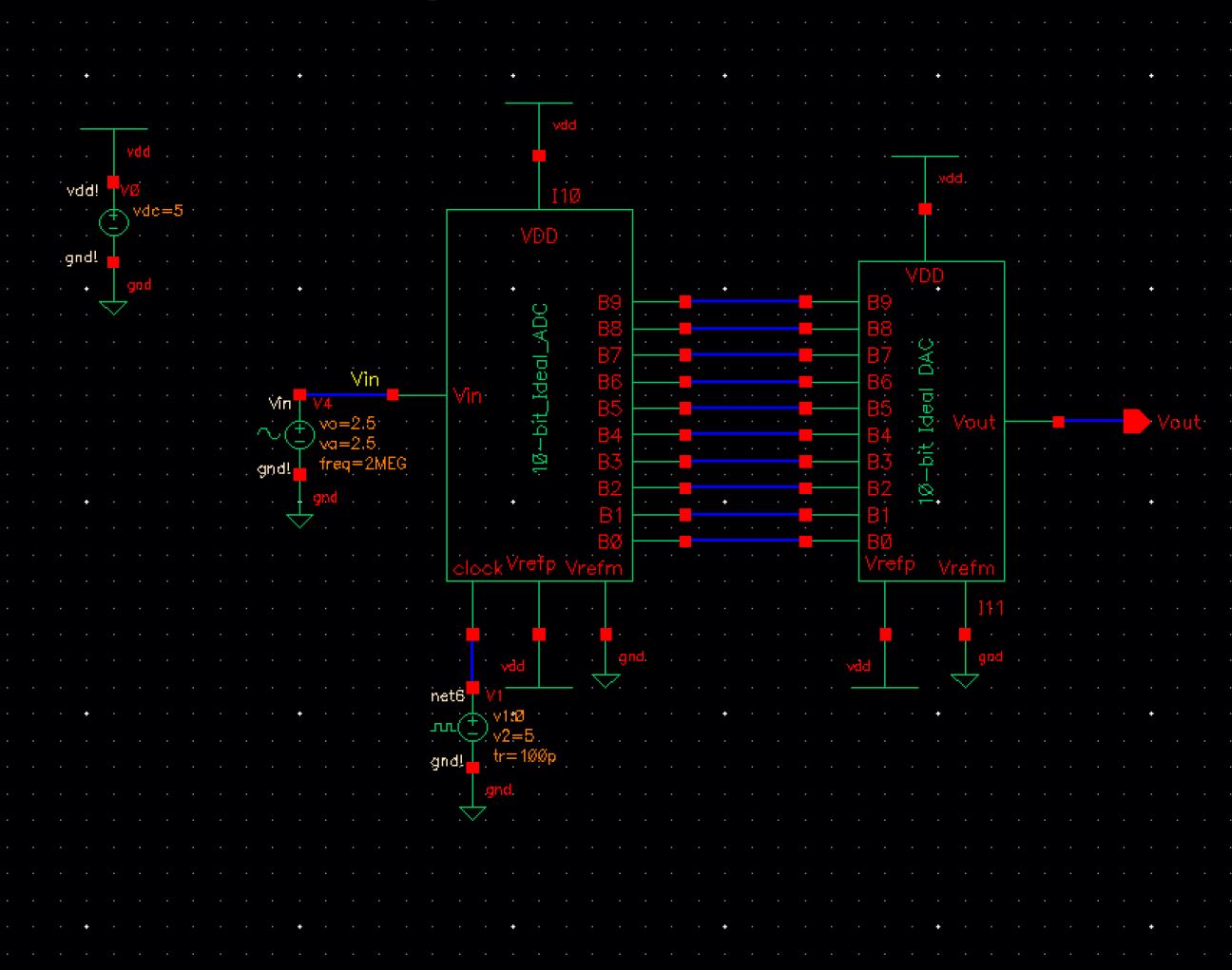
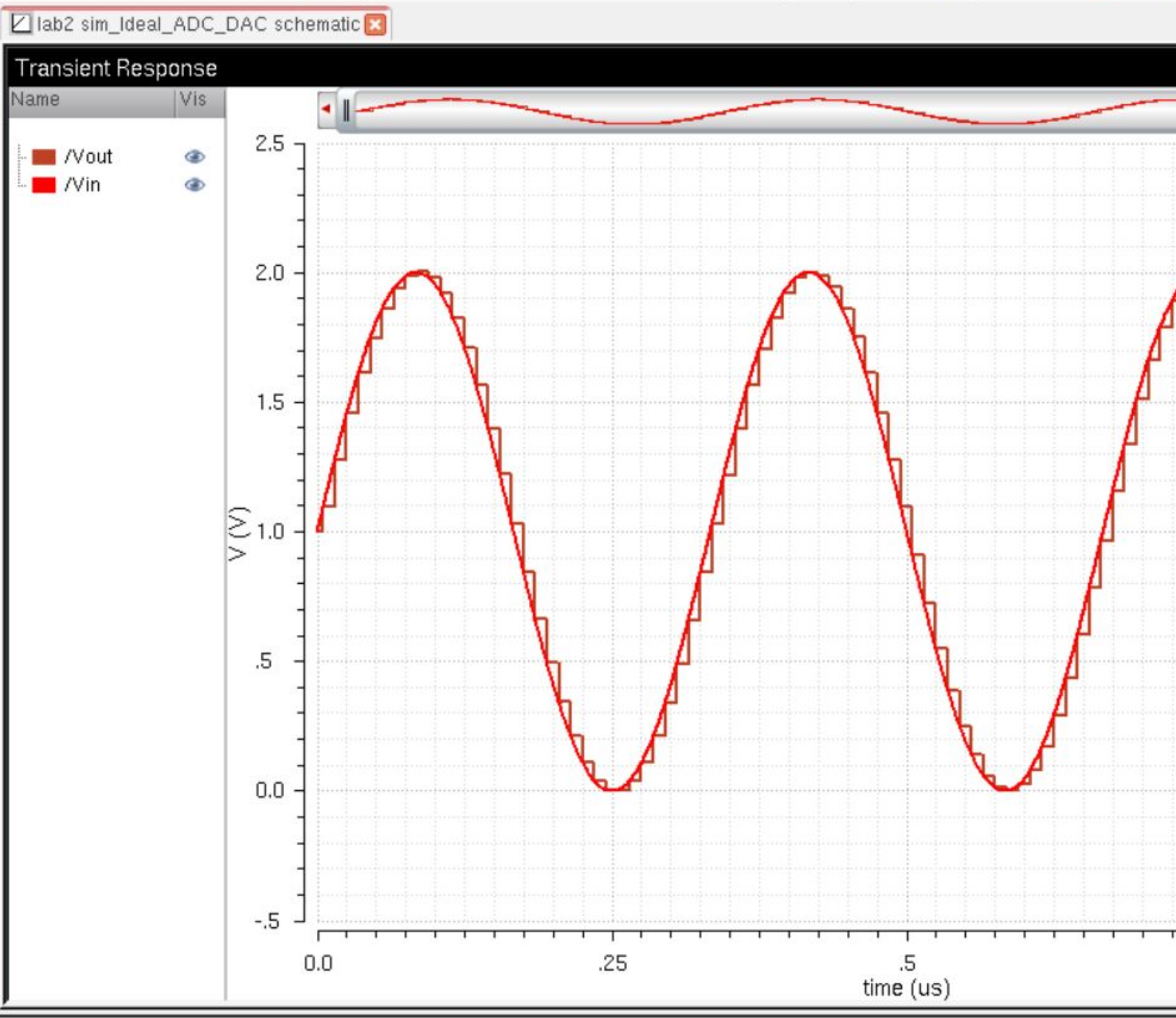
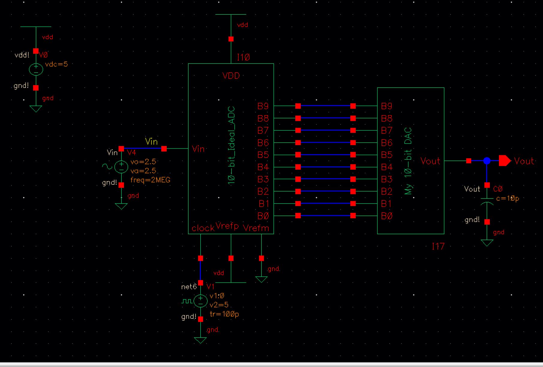
This is our original sim_Ideal_ADC_DAC schematic provided to us.
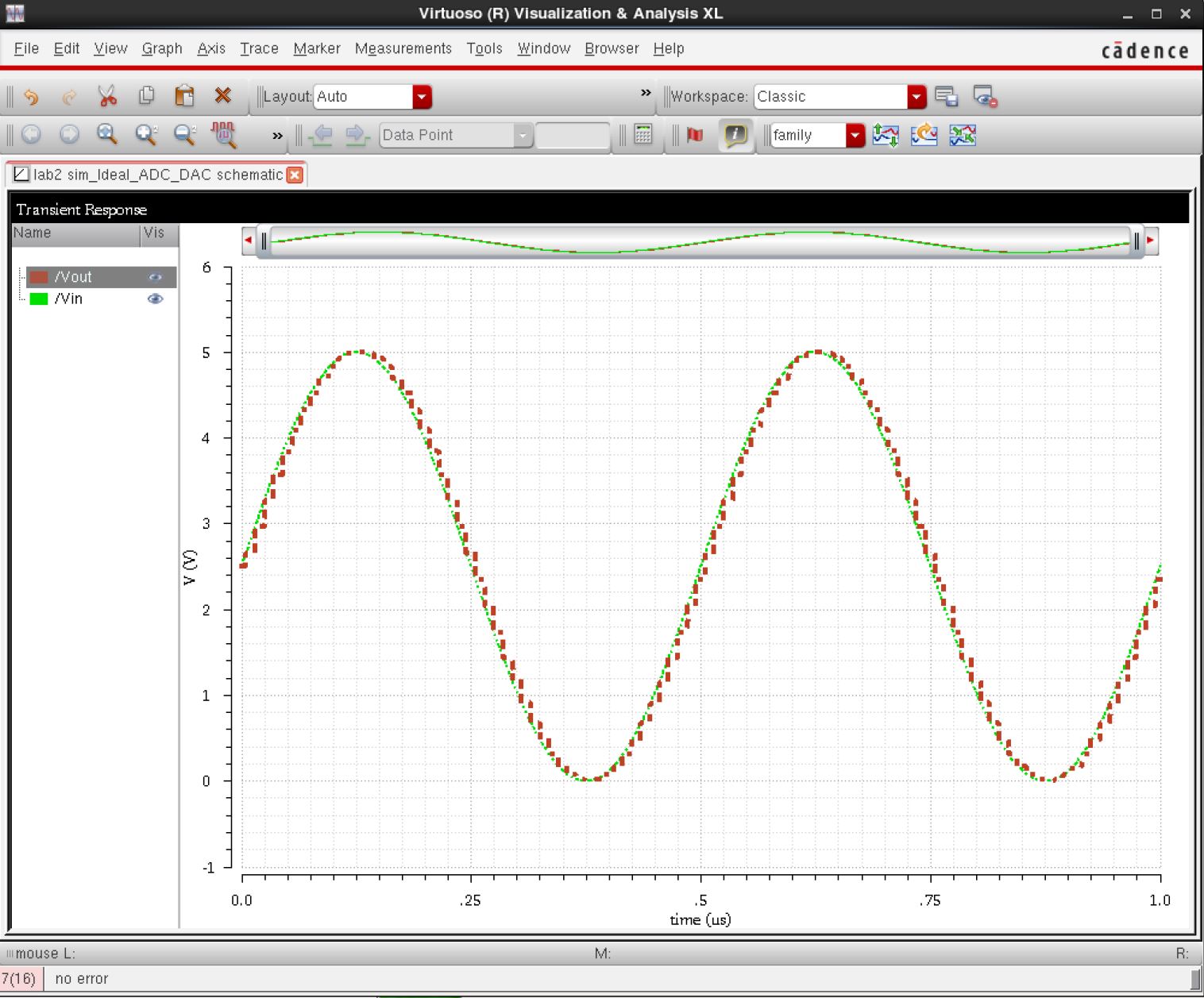
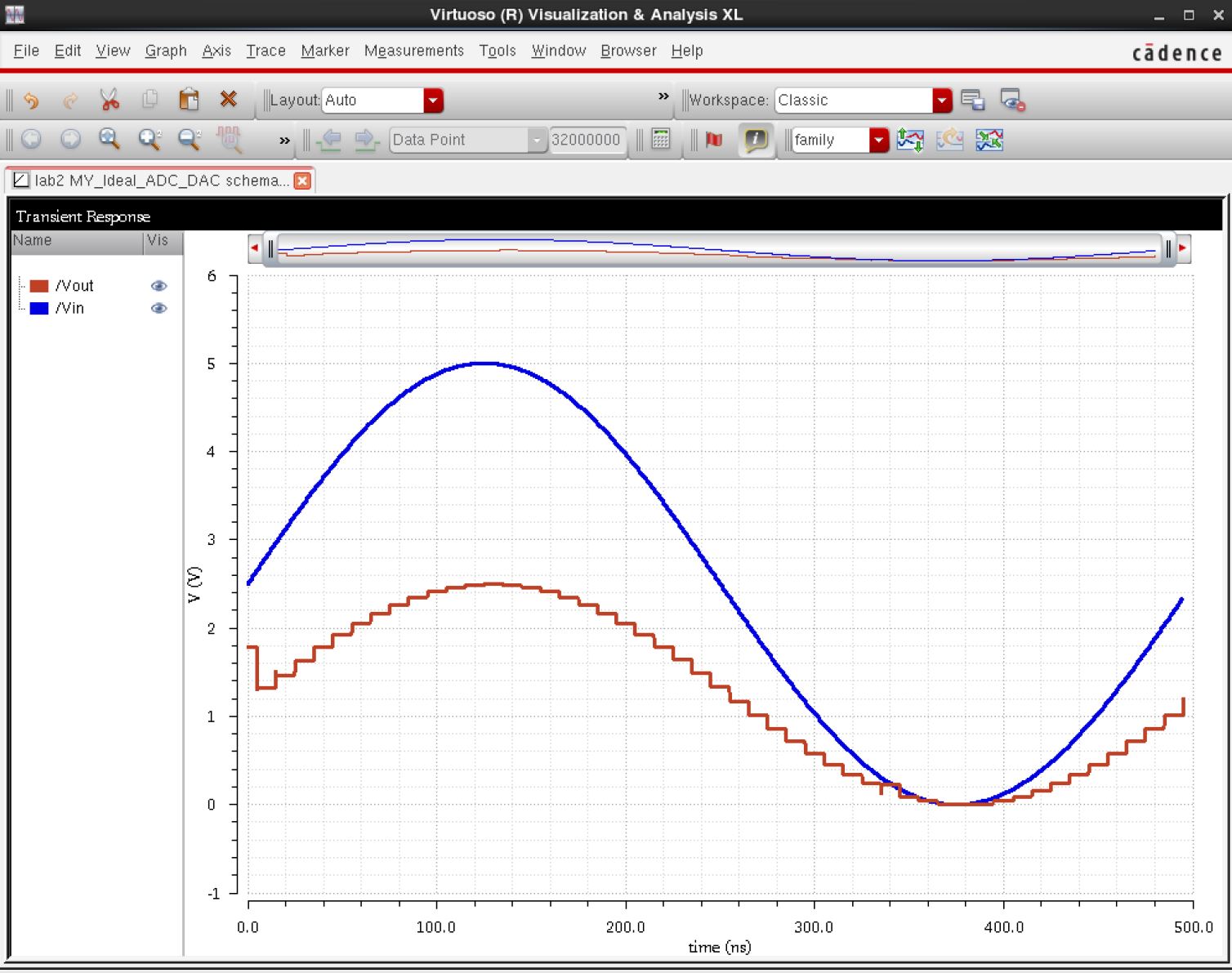
This is our corresponding transient response simulation of our original schematic.
Relationship between Vin, B[9:0], and Vout:
Vin
and Vout are interrelated because an analog signal Vin goes into the
ADC, the digital signal output of the ADC goes into the DAC, and the
output of the DAC is an analog signal of Vout. The B[9:0] constitutes a
10-bit binary value that is the output of the ADC due to the input
voltage (Vin).
LSB
The
least significant bit points to the rightmost bit in the digital input
or output word. This is the smallest possible change in the analog
output voltage.
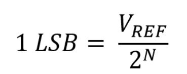
Since we used 10 bits, and the reference voltage is 5V, we have...

In
our ideal ADC and DAC system, the analog output (Vout) closely
follows the original analog signal input (in this case a sine wave).
Below, we used an offset of 1V and a max amplitude of 1V.
-------------------------------------------------------------------------------------------------------------------
POST LAB:
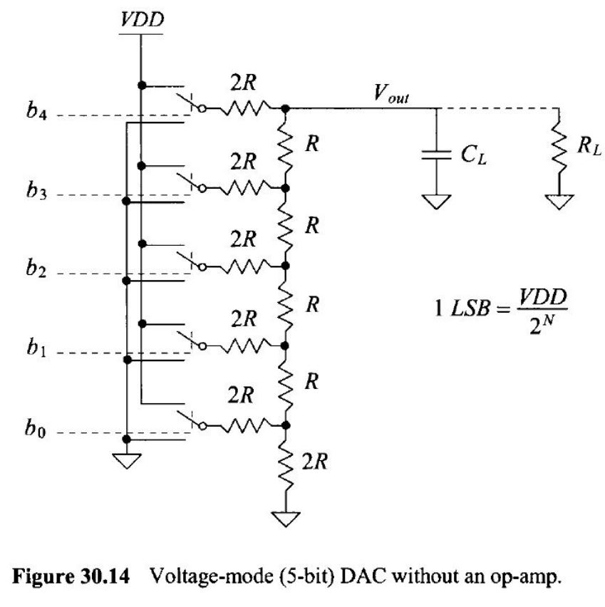
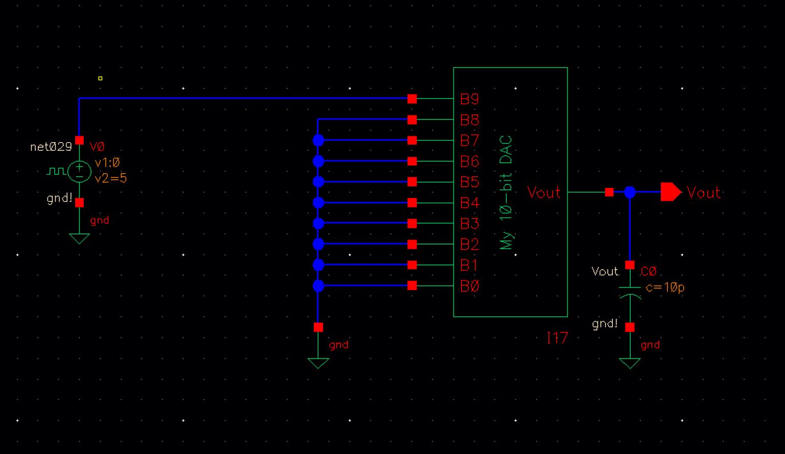
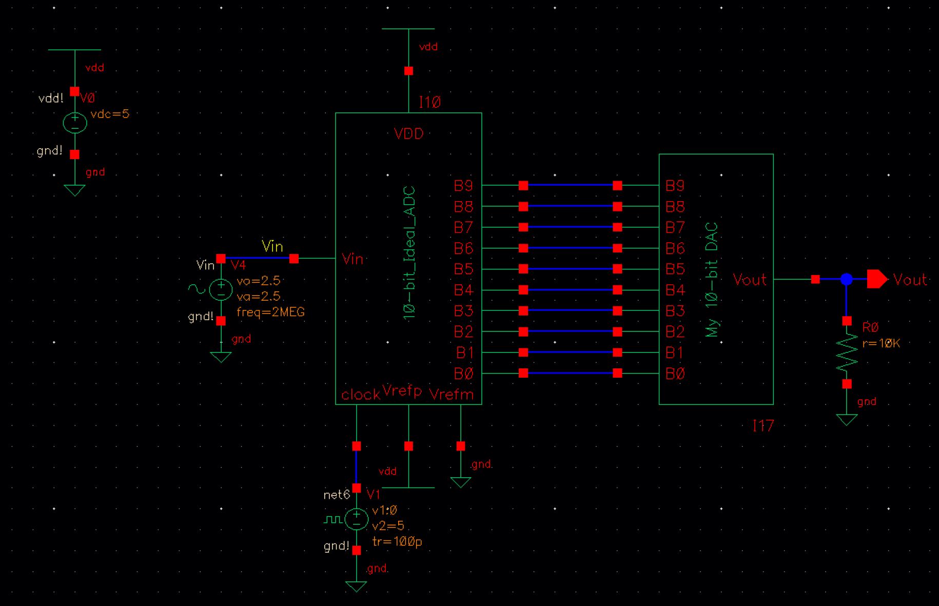
Our DAC follows the design of the schematic below.
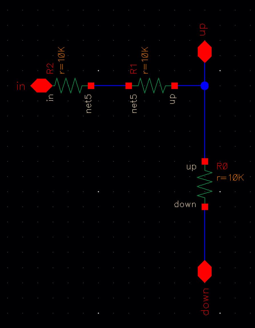
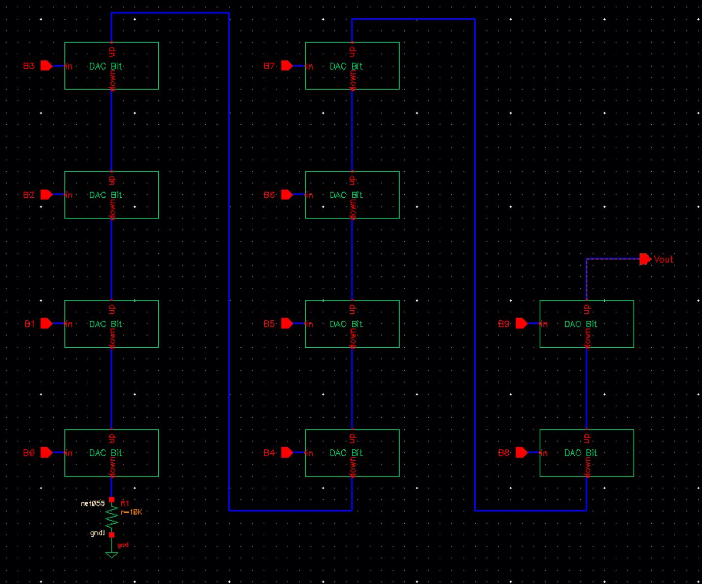
This is the bottom layer after descending all the way down to the schematic of our primitive sections of my DAC.
Ascending up a layer, we can see the DAC Bit symbols interconnected with one another creating the B[9:0] input to our DAC.
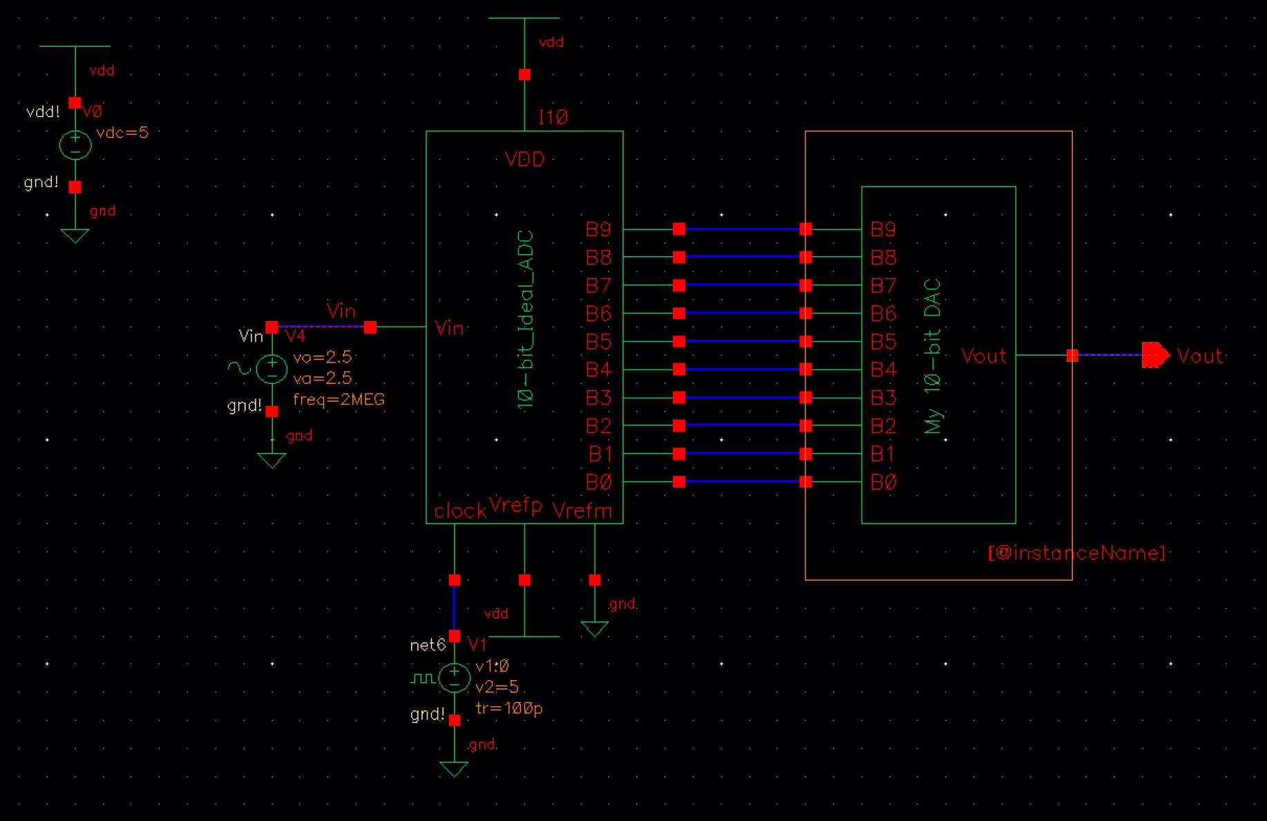
Ascending another layer up, we can see the final schematic all put together utilizing our new DAC, including the new symbol.
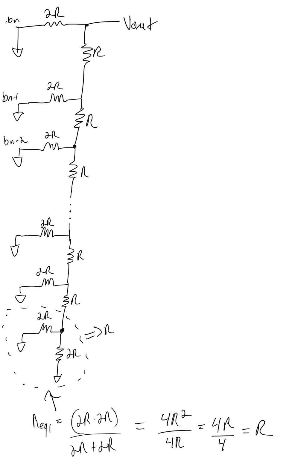
In order to obtain our total output resistance, we underwent the below calculations. After combining all subsections of our new schematic through our iterative process, we obtain an overall resistance of R, which equals 10kohms.
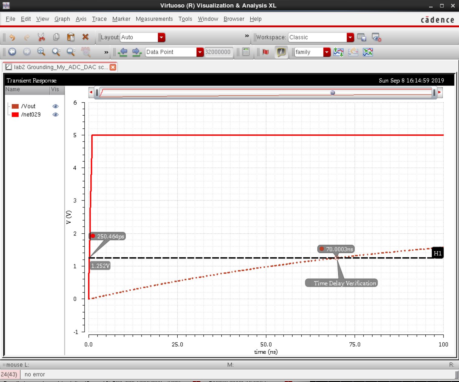
Calculating the delay to the circuit
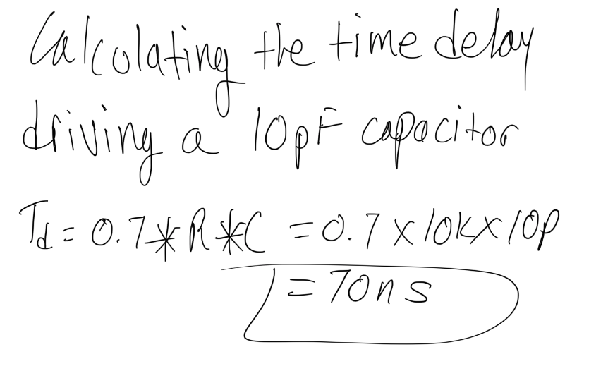
We
verfified this calculations through our simulation by grounding all of
the inputs of the DAC except for b9. After, we connected a 1V amplitude
pulse source to b9, and a 1 pF capacitor load was utilized as
well.
This simulation verifies our 70ns when the output is 50% of the max value.
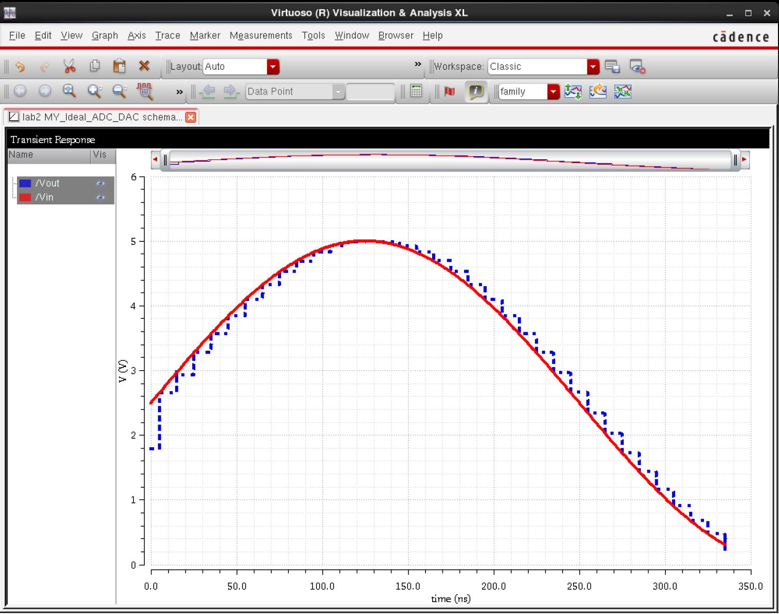
This is the simulation results of our new schematic. Again, the sine wave analog input closely follows the analog output of our new DAC we created.
------------------------------------------------------------------------------------------------------------------------------------------------
DRIVING LOADS
This the schematic of us testing our system with a 10k resistor load.
This
is the simulation result of us testing our testing with ONLY a 10k
resistor load. We can observe that our output is now half of its
original amplitude. This is due to the resulting voltage divider
between the output resistance of the DAC (10kohms) and the 10kohms load
resistance.
This is the schematic of our 10pF capacitor load added to our system.
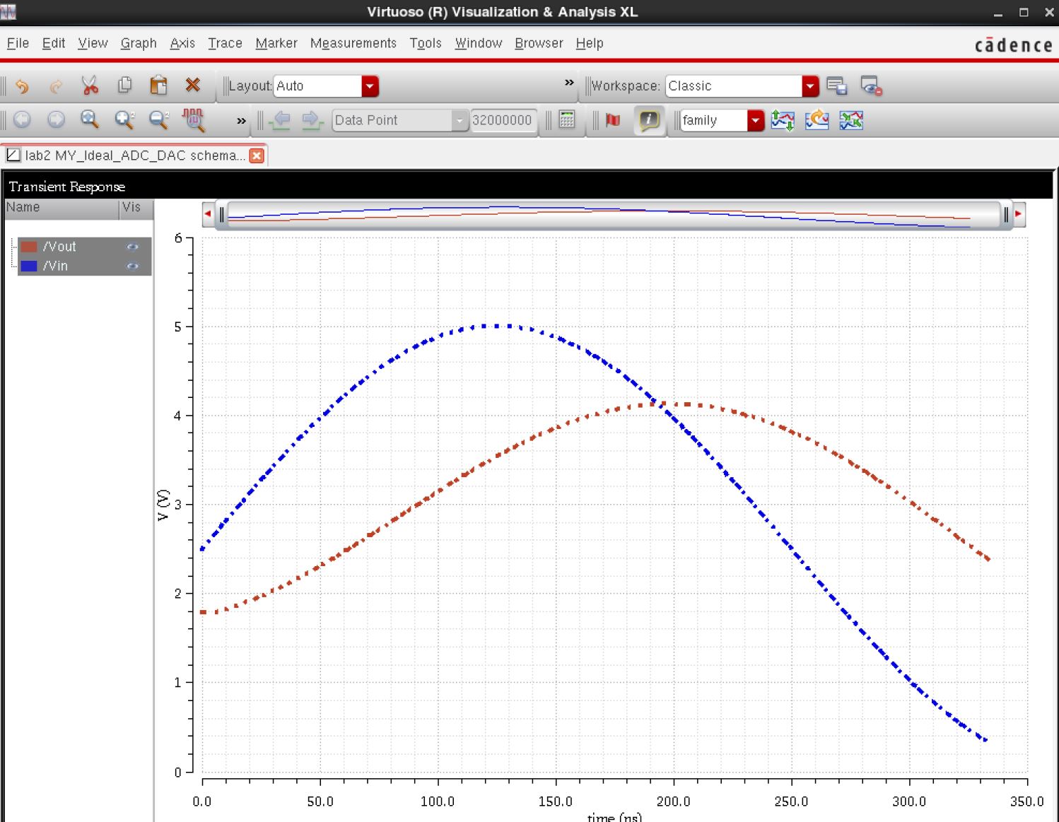
This is the simulation result of testing our capacitor load by itself.
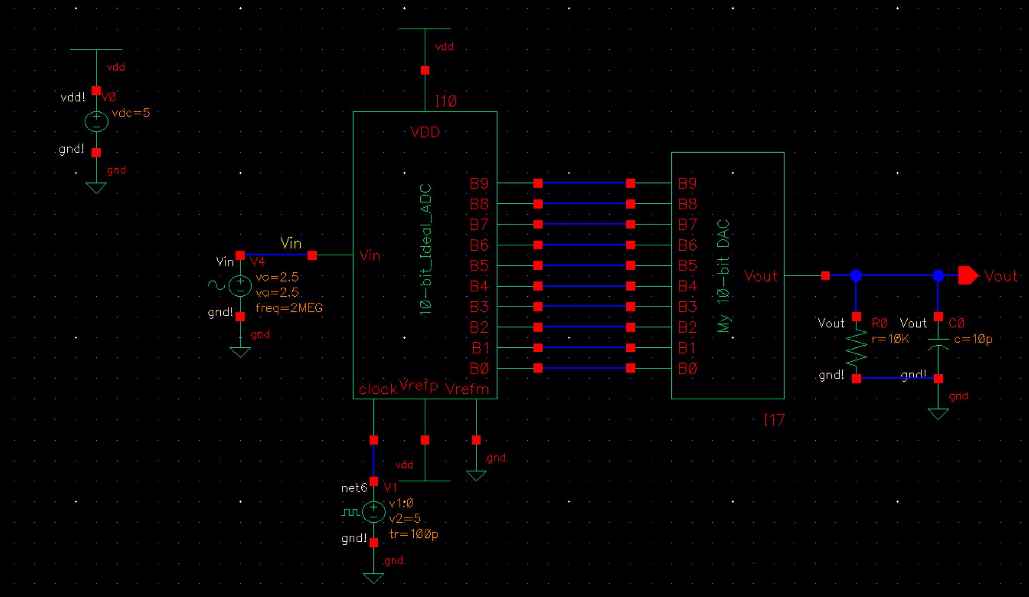
This is the schematic of our resistor and capacitor load added to our system.
This is the simulation result of our resistor and capacitor load added to our system. 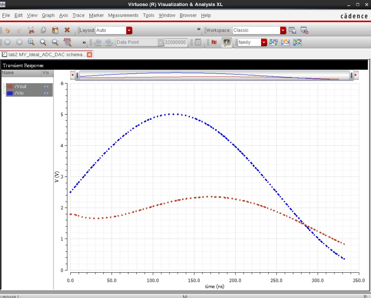
If the resistance of the switches is not small compared to R, then the input signal of the DAC would be a lot smaller.
Conversely,
better results are obtained when the resistance of the switches is
smaller compared to R, so Vout closely follows Vin.
In conclusion, we always want to back up our lab files (in this case to my personal Dropbox)...
Return to salazs3
Return to EE 421L Labs