Lab 4 - EE 421L
Authored
by Shaquille Regis
Email: regis@unlv.nevada.edu
September 25, 2019
Lab
description: We will be analyzing the IV characteristics and designing the layout for NMOS and PMOS
devices in the C5 process.
Pre-lab Work
1) Back-up all work and materials from the lab and course and read the lab procedure.
2) Go through Tutorial 2. Tutorial 2 is an overview of creating an NMOS and PMOS transistors, specifically the schematic
symbol view and layout as well as performing DRC, extraction and LVS.
Lab Work
1) Using the symbols created from Tutoral 2, generate 4 schematics and simulations.
a. Simulate ID vs VDS of an NMOS device for VGS varying from 0 to 5V in 1V steps while VDS varies from 0 to 5V in 1mV steps.
Use a 6u/600n width:length ratio.

Simulation Results

b.
Simulate ID vs VGS of an NMOS device for VDS = 100mV where VGS varies
from 0 to 2V in 1mV steps. Again use a 6u/600n width:length ratio.

Simulation Results

c. Simulate ID vs VSD of a PMOS device for VSG varying from 0 to 5V in 1V steps while VSD varies from 0 to 5V in 1mV steps.
Use a 12u/600n width:length ratio.

Simulation Results

d.
Simulate ID vs VSG of a PMOS device for VSD = 100mV where VSG varies
from 0 to 2V in 1mV steps. Again use a 12u/600n width:length ratio.

Simulation Results

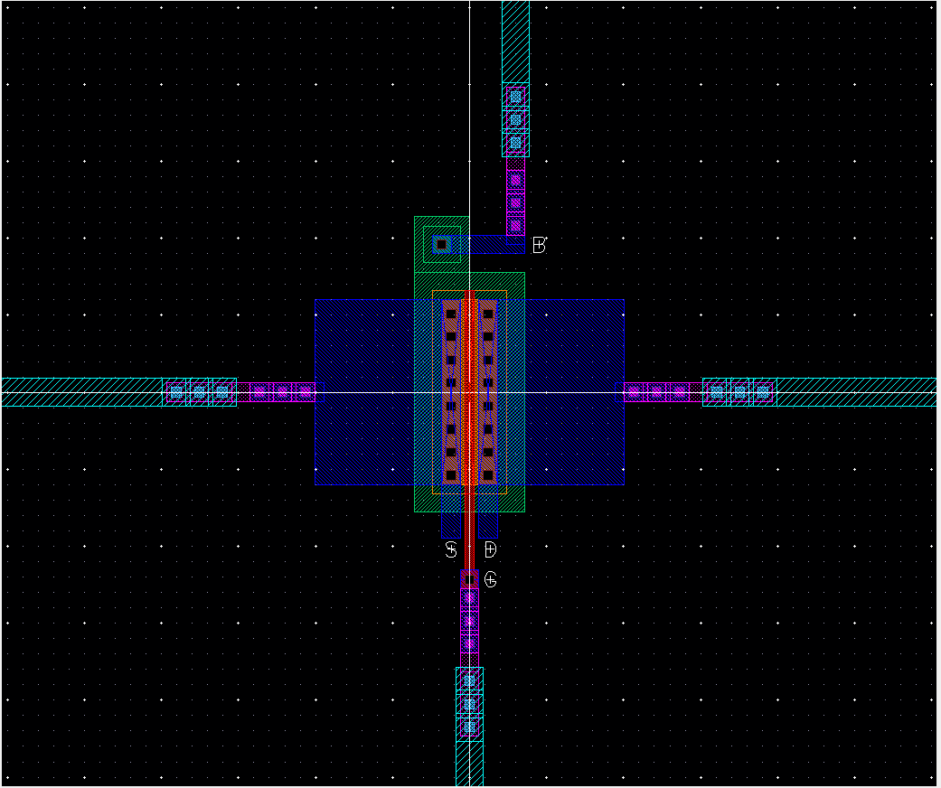
2) Layout a 6u/0.6u NMOS device and connect all 4 MOSFET terminals to probe pads.
The
layout comprises the nmos layout from the NCSU_TechLib_ami06 library. A
ptap layout from the same library is also needed as the pin for the
body.
An
m1_poly layout is connected to the poly1 gate. Pins for the terminals
"S", "D", "G" and "B" (gnd!) are created with the metal1 layer. The
metal1 pins are
connected up to metal2 then through metal3 using m1_m2 and m2_m3 layouts to connect to the probe pads at the metal3 layer. The probe pads are found
on the lab 4 instructions page in the linked lab4.zip resource.
Transistor View

Full Layout

DRC verification

LVS

3) Layout a 12u/0.6u PMOS device and connect all 4 MOSFET terminals to probe pads.
The
layout comprises the pmos layout from the NCSU_TechLib_ami06 library.
An ntap is used for the body of the transistor. An m1_poly layout
is connected to the poly gate of the transistor. Pins for the terminals "S", "D", "G" and "B" (gnd!) are created with the metal1 layer. The metal1 pins are
connected up to metal2 then through metal3 using m1_m2 and m2_m3 layouts to connect to the probe pads at the metal3 layer like the NMOS.
Transistor View
Full layout
DRC Verification

LVS

As always remeber to backup all work and lab materials to zip and email.
End of Report
Return to Shaq's Labs