Lab 2 - ECE 421L Fall 2019
Cody Jones,
Jonesc30@unlv.nevada.edu
8/31/2019
Prelab
1)
Download the lab2 file, unzip it and add the directory to cds.lib text file so it can be found.
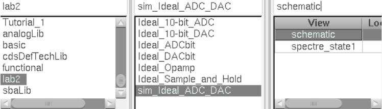
Open the lab2 library to get the sim_ideal_ADC_DAC cell and open the schematic.
Once the schematic is open, run the simulation to get the results for the ADC to DAC.
2)
The
ADC uses the reference voltage to create a digital signal where the DAC
takes that digital signal and turns it into an analog signal. The
circuit cannot use anything more than 5V. The 10-bit DAC breaks the
total voltage into 10 components that are represented in different bits
of the signal. The least significant bit pin will be 00 0000 0001. We
can find the LSB by VDD/(2^N), which will give us the minimum voltage.
Lab
description
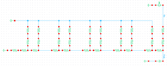
In this lab, we will be using n-well resistors to implement a 10-bit DAC.
1)
The schematic of the 10-bit DAC with n-well resistors of 10K.

2)
To
get the output resistance of the DAC, we short the pins. Then we will
see that there are two resistors, that are both 10k, that are in
series. The two resistors are parallel with another set of two
resistors, that are both 10k, that are in series. The parallel
combination is R, 10k. This will be a repeated process since all the
resistors are 10k in the circuit until we get to the top of the DAC
circuit where we do the process one last time to get a final output
resistance of R, 10k.
3)
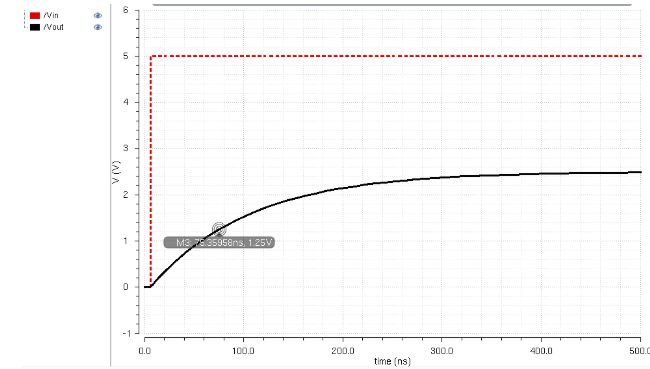
Here
is all the DAC inputs grounded except B9 that has a pulse source from 0
to 5V with a resistor as the load of 10K. The B9 input will give off a
2.5V for Vout. So, at 1.25V we will have our time cycle of 0.7RC =
0.7(10K)(10p) = 70ns.
4)
Made
a new symbol for my DAC and changed the DAC that was in the
sim_ideal_ADC_DAC to sim2_ideal_ADC_DAC that has my DAC. Below you can
see that my DAC is call My 10-bit DAC.
5)
Driving a 1pF capacitance
Driving a 10K load resistance
Driving both a 10K resistor and a 1pF capacitor
Since
the output load of the DAC is already 10K resistance, when we add
another 10K load we create a voltage divider. The output voltage is
half of the original output voltage which was the same as the input
voltage.
6)
If
the resistance of the switches isnt small compared to R, when we do the
parallel combination we won't get R because we will now have 2R+(the
switches resistance) in parallel with 2R.
Return to EE 421L Labs


