Project - ECE 421L
Project
Design a circuit that takes a 9-11 MHz clock signal and generates a 36-44 MHz clock signal. In other words, design x4 clock multiplier. The input clock is multiplied by 4 and output. Assume the input clock signal has a 50% duty cycle.
Designing x4 clock multiplier
The x4 clock multiplier is made up of two x2 clock multiplier, as seen in the schematic below. The schematic contains two XOR gates and two delay buffers.

XOR
I designed the two XOR gates to be the same as lab six except that pmos is 12u/.6u, and nmos is 6u/.6u. The schematic and layout are shown below.


Delay
I designed the two delay buffers to have two specific amount of delay using weak inverters. The weak inverter is created using pmos that is 12u/7.2u and nmos that is 6u/7.2u. I choose the lengths of the MOSFET to be very long to avoid having to layout to many MOSFETs. The schematic and layout of the weak inverter are shown below.

First Delay Buffer
The first delay buffer was designed to have a 25ns delay since the input the first x2 clock multiplier is around 10MHz. This delay was achieved by using six weak inverters and then a few large inverters to smooth the output, as shown in the schematic and layout below.


These images are the result of testing the delay buffer.


Second Delay Buffer
The second delay buffer is design similar to the first, except there are three weak inverters instead of six. This is done to have a delay of 12ns since the input of the second x2 clock multiplier is around 20MHz.


This image is the result of testing the delay buffer.

Testing x4 clock multiplier
I tested the x4 clock multiplier with frequency varying for 9MHz to 11MHz and VDD varying for 4.5V to 5.5V. From testing, I found that when VDD is outside this range, the output of the multiplier is not in the range of 36MHz to 44MHz. The frequency of 36MHz to 44MHz means a period of 22.7ns to 27.8ns.

Results:
VDD Frequency | 4.5V | 5.0V | 5.5V |
| 9MHz | 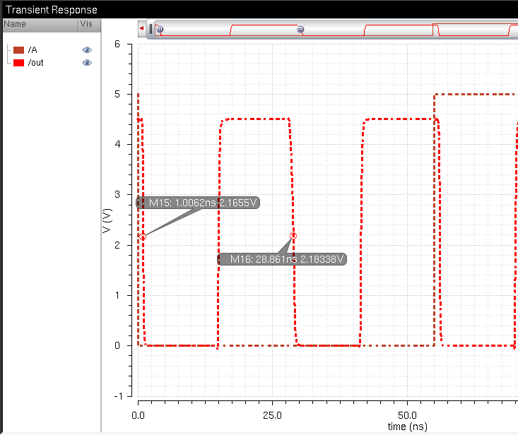 27.8ns period or 36MHz | 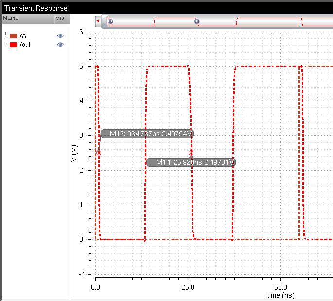 25ns period or 40MHz | 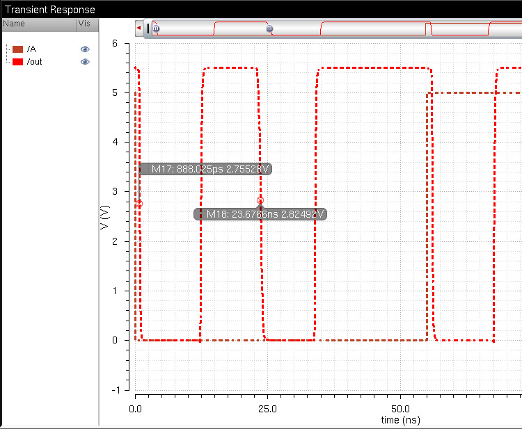 22.8ns period or 43.9MHz |
| 10MHz | 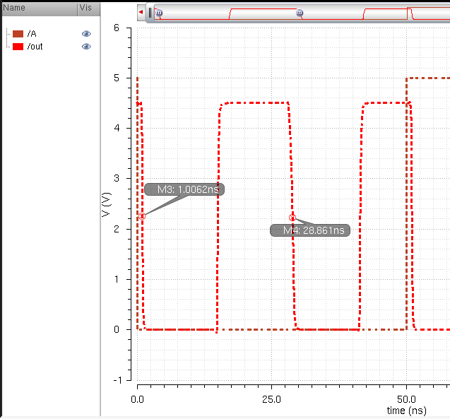 27.8ns period or 36MHz | 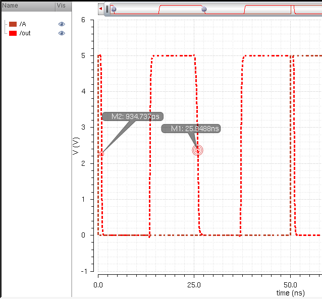 25ns period or 40MHz | 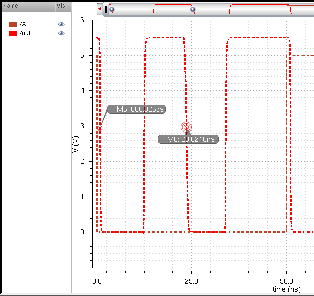 22.8ns period or 43.9MHz |
| 11MHz | 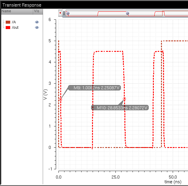 27.8ns period or 36MHz | 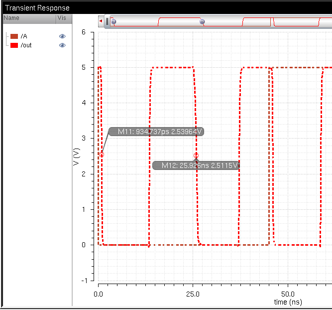 25ns period or 40MHz | 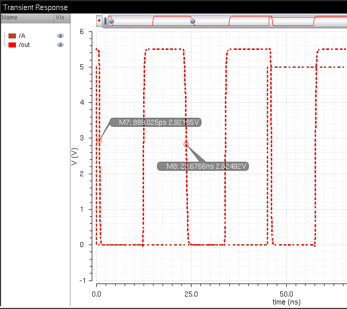 22.8ns period or 43.9MHz |
Layout of x4 clock multiplier
The layout of the clock multiplier is simply putting the layout of XORs and Buffer delays together

DRC:

LVS:
