Lab Final Project - EE 421L
Authored
by Adrian Angelo G Fuerte
Rebelmail: fuerta1@unlv.nevada.edu
November 13, 2019
Project Description
- Design a circuit that takes a 9-11
MHz clock signal that generates a 36-44 MHz clock signal. In other
words, design a x4 clock multiplier. The input clock is multiplied by 4
and output. Assume the input clock signal has a 50% duty cycle.
-
First half of the project (schematic and design discussions) of your
design and an html report detailing operation (including simulations),
is due at the beginning of lab on Nov. 13.
-
Your design report in html should show various clock input frequencies
and VDD voltages to show it works. Put your report (proj.htm) in a
folder called /proj in your directory at CMOSedu and link your
index.hym page. Dr. Baker will go over your design win you (in person),
including running simulations, when lab meets on Nov. 13.
- Second half of the project, a verified layout and documentation (in html), is due at the beginning of lab on Nov. 20.
PART 1: SCHEMATIC AND DESIGN DISCUSSION
Note: Click on the images to enlarge and get a clearer view of them
Schematic Overview
-
In order to generate an output clock signal that is quadruple (4x) of
our input signal, the circuit that I will be using is shown below,
which consists of two buffers and two XOR gates. Inside each of the
buffers contains a total of 6 inverters, 3 of these inverters are used
to delay the input signal and the other 3 are to make the rising and
falling edge of the output to be sharper/steeper. To have faster
edges, the lengths of the inverters have to be small as indicated in
the following equation: C = Cox'*W*L.
| Schematic Overview |
 |
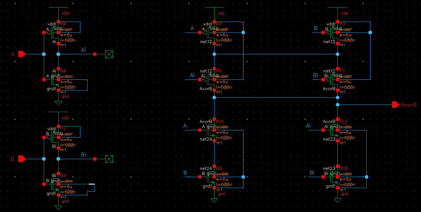
XOR Gate
For
the XOR gate that is used in this project, I will be using the one that
we have designed in Lab 6. The NMOS and PMOS widths and lengths are
6u/600n. The XOR gate is used because of its functionality, whenever
Input A or Input B are high (1), the output is also high (1), the
output is only low (0) when both Input A and Input B are also low
(0).
XOR Gate Truth Table
| Input A | Input B | Output |
| 0 | 0 | 0 |
| 0 | 1 | 1 |
| 1 | 0 | 1 |
| 1 | 1 | 0 |
XOR Gate Schematic and Symbol
| Schematic | Symbol |
|  |
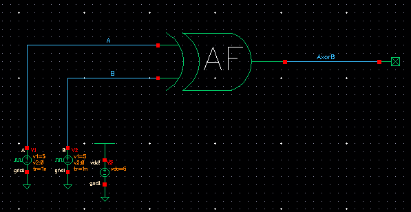
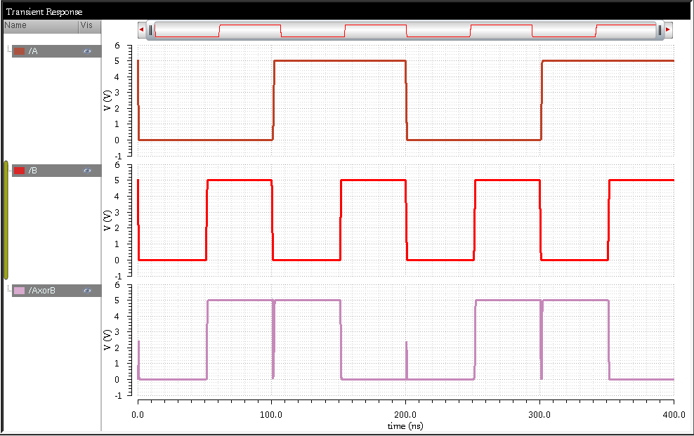
XOR Gate Simulation Schematic and Result
| Simulation Schematic | Simulation Result |
|  |
FIRST BUFFER (x2 Frequency)
To get started on the project, I first had to design a buffer that could output a x2 frequency for my 1st XOR
gate. My buffer will take the input from the XOR gate's 1st input (A)
and send it through the buffer and input it to the XOR gate's 2nd input
(B) and output it into the first XOR gate as seen in the schematic
overview above. I also used m = 4 as my size factor for my first
buffer.
Delay buffer (Left Side)
-> My delay buffer consists of 3 inverters. The PMOS has a dimension
of 12u/7.2u (W/L) and my NMOS has dimensions of 6u/7.2u (W/L), I used a
length of 7.2u for my inverters to achieve the goal of having a 50%
duty cyle for the output signal and in order to get the 50% duty cycle,
the delay time has to be approximately 25ns when the signal is either
high or low.
Short Length buffer (Right Side)
-> This buffer also consists of 3 inverters. The PMOS has a
dimension of 12u/.6u (W/L) and my NMOS has dimensions of 6u/.6u (W/L).
I used minimum lengths for these inverters in order to achieve a
sharper/faster edge and lower the capacitance.
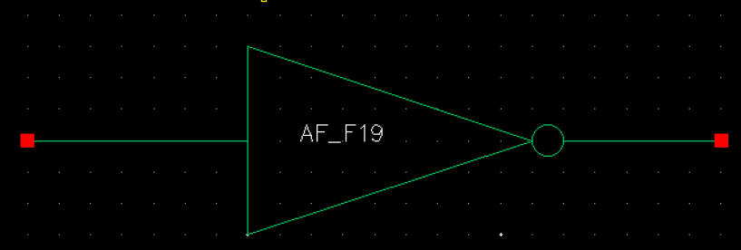
First Buffer Schematic and Symbol
| Buffer Schematic | Buffer Symbol |

| 
|
Simulation Schematic and Result
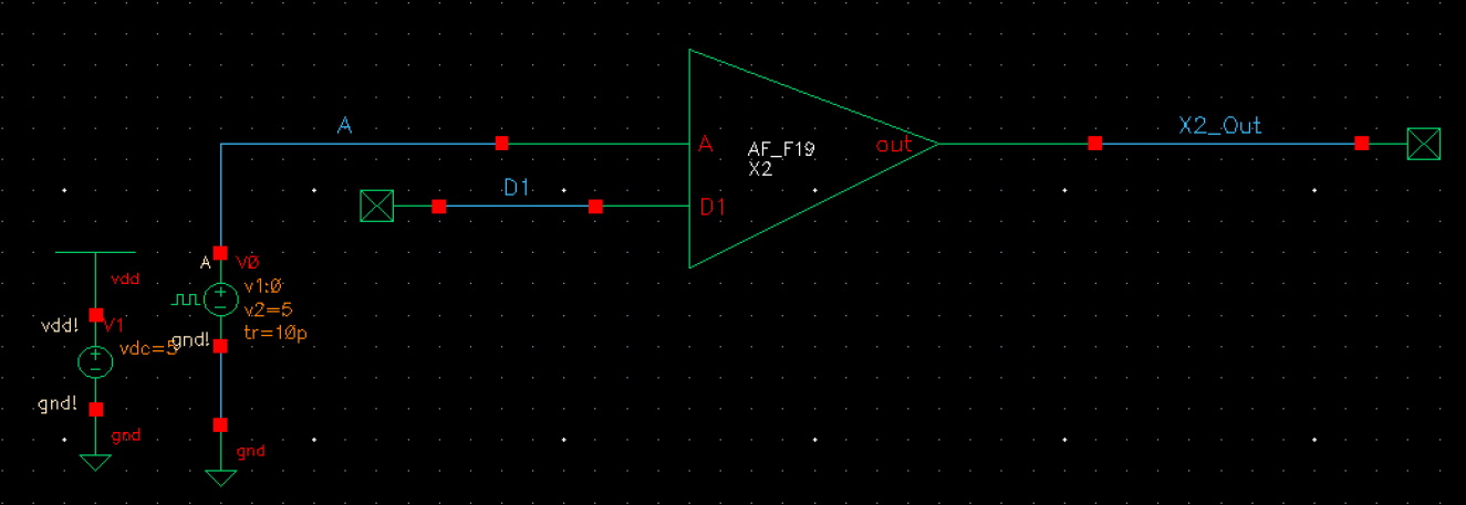
-> For the simulation I made a simulation schematic and simulated my designs using this schematic.
For
the simulation of my first buffer and XOR gate, I used a period of
100ns (10MHz) for the input signal. As can be seen in the
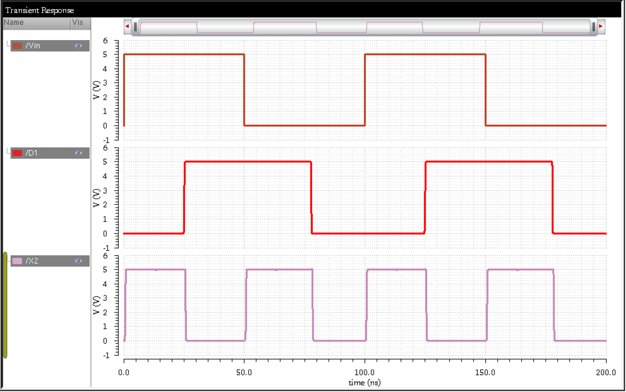
simulation result, the delay is about 25ns.
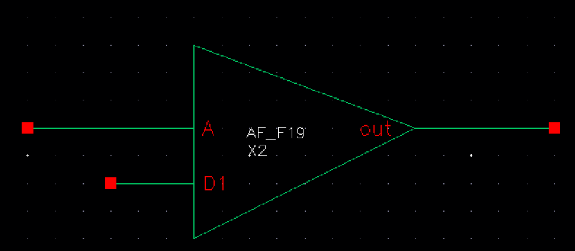
D1 -> Delay
| Schematic | Simulation Symbol |
 |  |
Simulation Result:
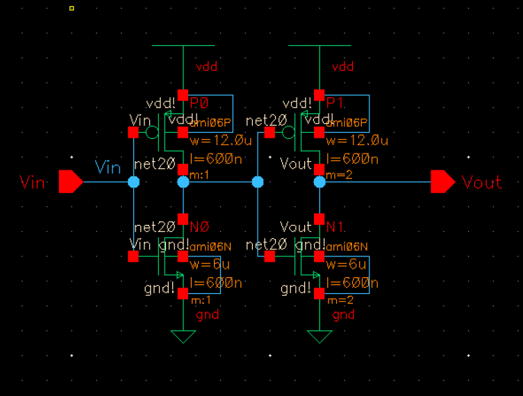
The edges for X2_Out are not sharp, so I added a small buffer with
minimum lengths to the output. PMOS has dimensions of 12u/.6u and NMOS
has dimensions of 6u/.6u.
| Simulation Schematic | Simulation Result |
 |  |
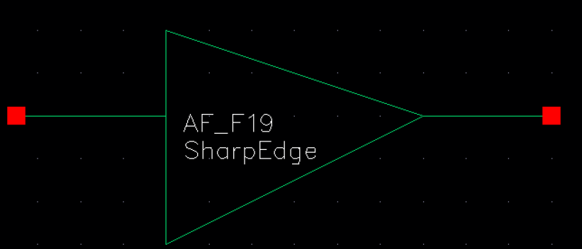
Small Buffer Schematic and Symbol (Used in the output of 1st XOR and 2nd XOR gates)
| Small Buffer Schematic | Small Buffer Symbol |
 |  |
Simulation Result of X2 Circuit (After adding small buffer)
| Simulation Result |
 |
SECOND BUFFER (X4 FREQUENCY)
-> For my second buffer, I had to design a buffer that takes the output from the x2 frequency of my 1st XOR
gate as one of the inputs and also take that x2 frequency output
through the 2nd buffer and outputs a 4x frequency as seen in the
schematic overview at the beginning of this report. I used a size
factor of 8 for this buffer.
Delay Buffer (Left Side)
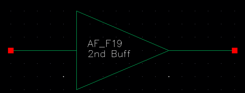
-> The delay buffer consists of 3 inverters. The PMOS have
dimensions of 12u/3.45u (W/L) and the NMOS have dimensions of 6u/3.45u
(W/L).
Notice the lengths are smaller than the first buffer, this is due to
the delay time to be smaller than the first buffer. To achieve the goal
of having a 50% duty cyle for the output, the delay time has to be
approximately 12ns.
Short Length Buffer (Right Side) -> This
buffer also consists of 3 inverters. The PMOS has a dimension of
12u/.6u (W/L) and my NMOS has dimensions of 6u/.6u (W/L). I used
minimum lengths for these inverters in order to achieve a
sharper/faster edge and lower the capacitance.
2nd Buffer Schematic and Symbol
| Second Buffer Schematic | Second Buffer Symbol |

|  |
Simulation of x4 Frequency Schematic and Result
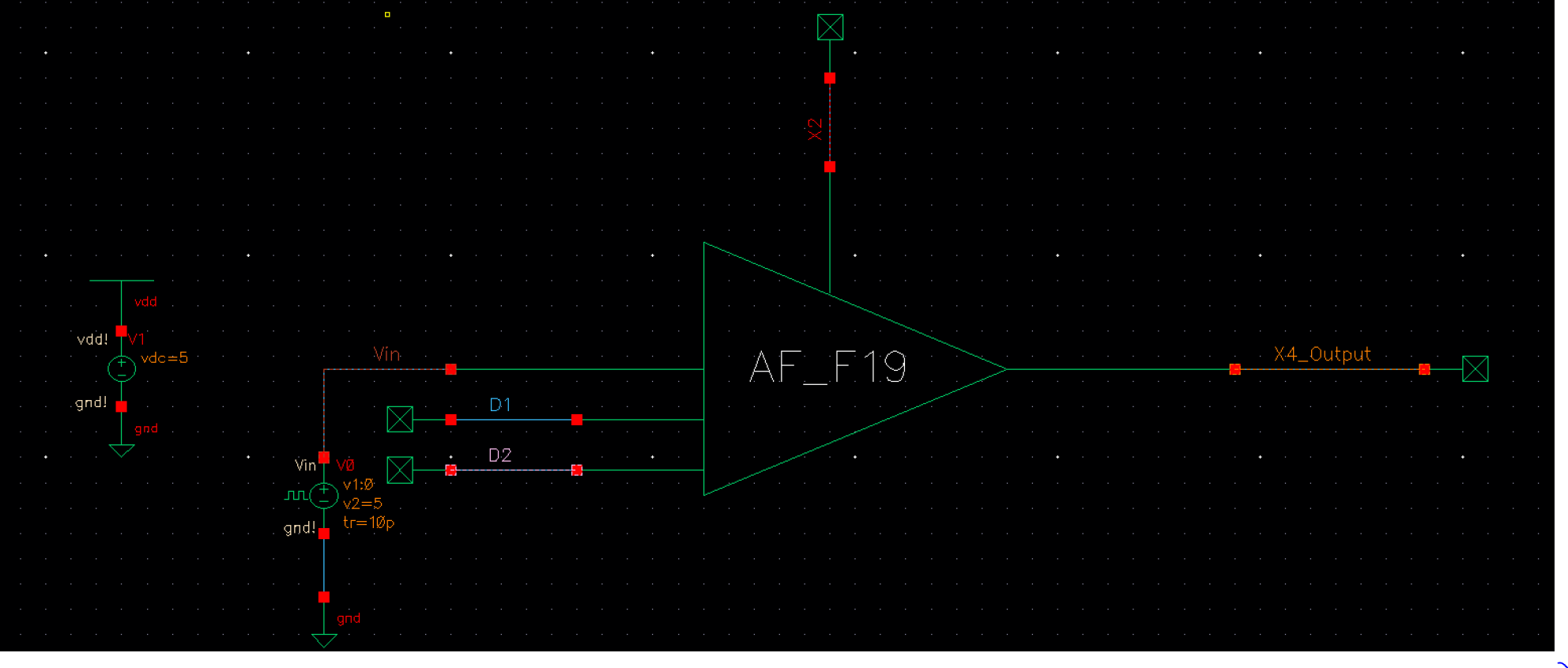
Note: The following schematic used for simulation purpose only. I also added the small buffer at the output in order to get a sharper edge.
->
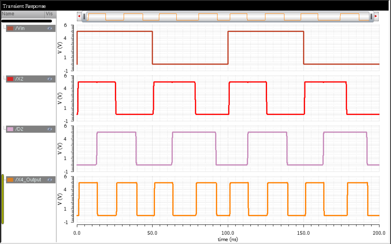
For the simulation of just the x4_Output I only plotted the Input (Vin),
X2(x2 frequency output), D2 (2nd delay), and X4_output (x4 frequency
output)
| Schematic | Simulation Schematic |
 | 
|
Simulation Result (Without small buffer)
| Simulation Result |
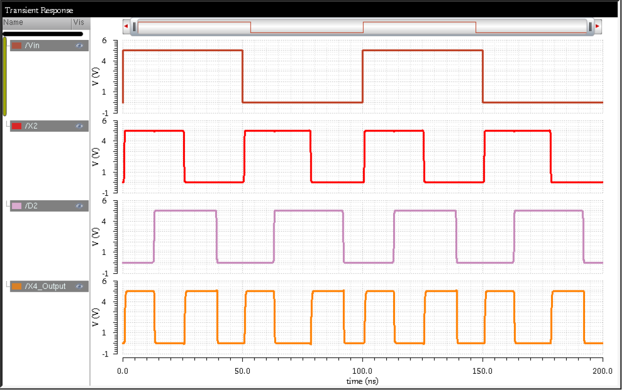 |
Simulation Result (With Small Buffer): Notice, the edges of the x4_output is sharper
| Simulation Result |
 |
Simulations For Different Frequencies and VDD
| Frequency, Period and VDD Values | Simulation Results |
Frequency: 9 MHz
VDD: 4V
Period: 111ns | 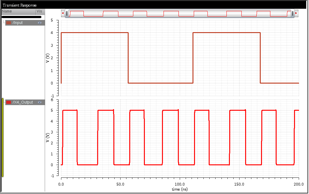 |
Frequency: 9 MHz
VDD: 4.5V
Period: 111ns | 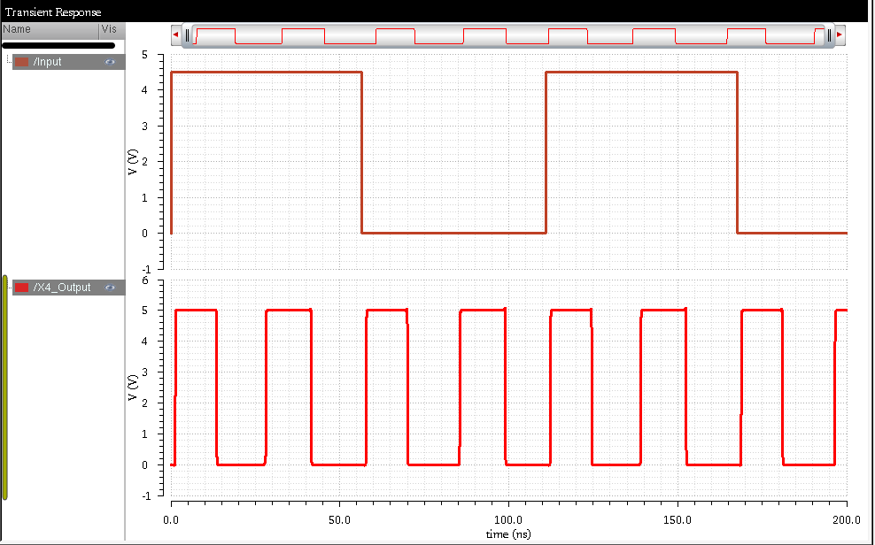 |
Frequency: 9 MHz
VDD: 5V
Period: 111ns | 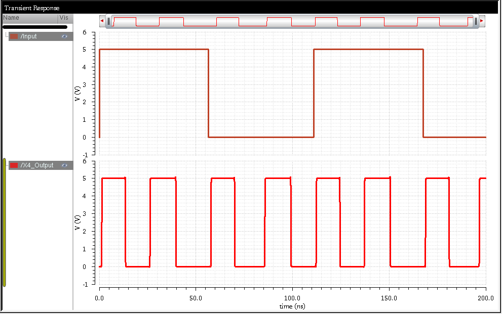 |
Frequency: 9 MHz
VDD: 5.5V
Period: 111ns |  |
Frequency: 9 MHz
VDD: 6V
Period: 111ns | 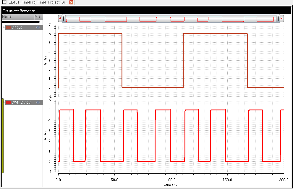 |
Frequency: 9 MHz
VDD: 6.5V
Period: 111ns | 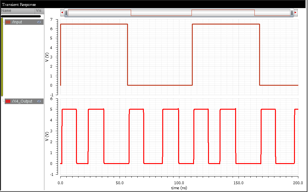 |
Frequency: 9 MHz
VDD: 7V
Period: 111ns | 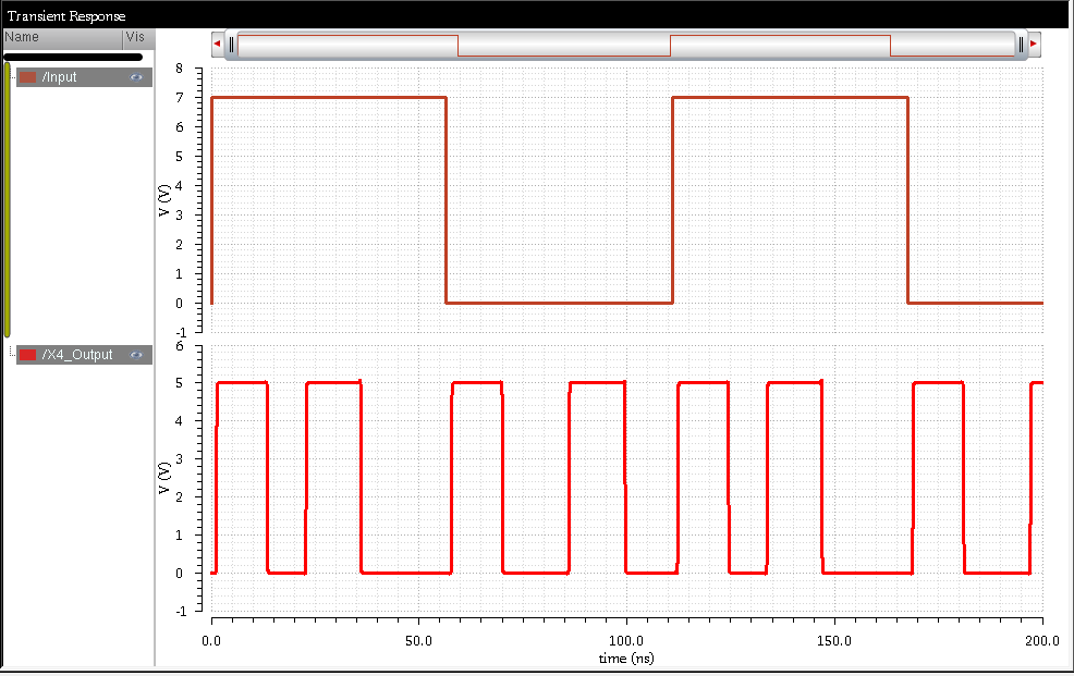 |
| Frequency, Period and VDD Values | Simulation Results |
Frequency: 10 MHz
VDD: 4V
Period: 100ns | 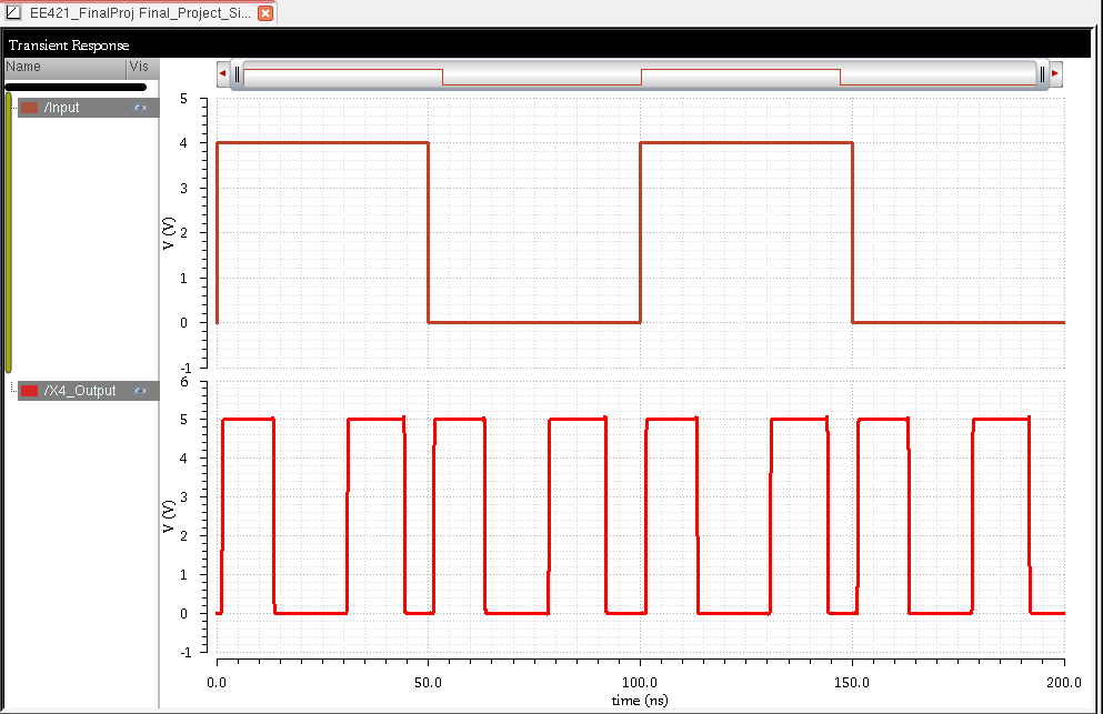 |
Frequency:10 MHz
VDD: 4.5V
Period: 100ns | 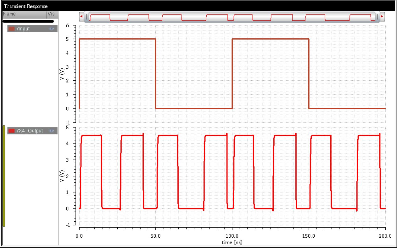 |
Frequency: 10 MHz
VDD: 5V
Period: 100ns | 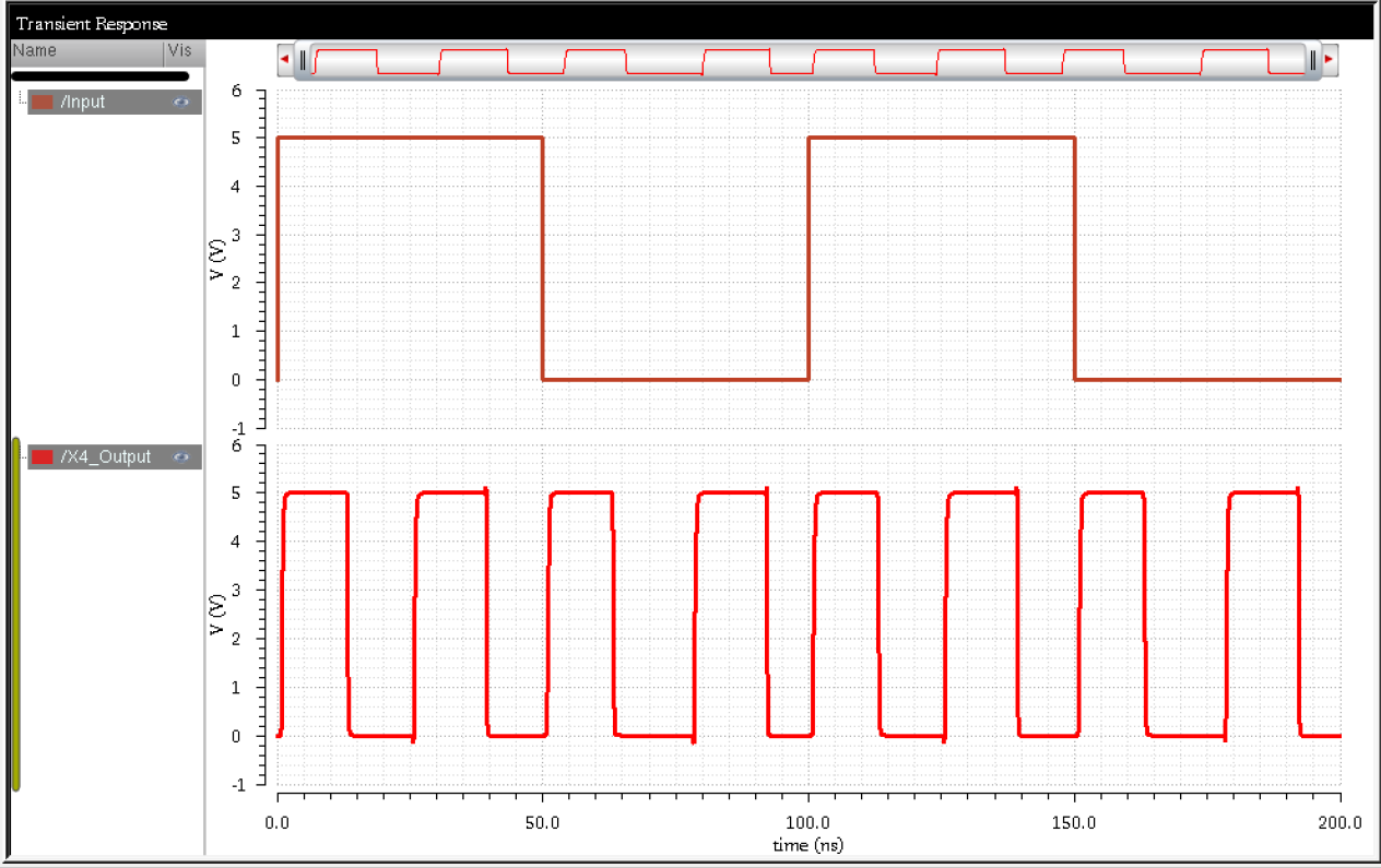 |
Frequency: 10 MHz
VDD: 5.5V
Period: 100ns | 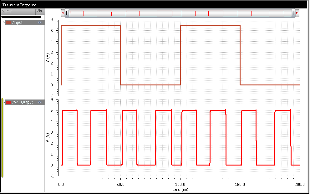 |
Frequency: 10 MHz
VDD: 6V
Period: 100ns |  |
Frequency: 10 MHz
VDD: 6.5V
Period: 100ns |  |
Frequency: 10 MHz
VDD: 7V
Period: 100ns | 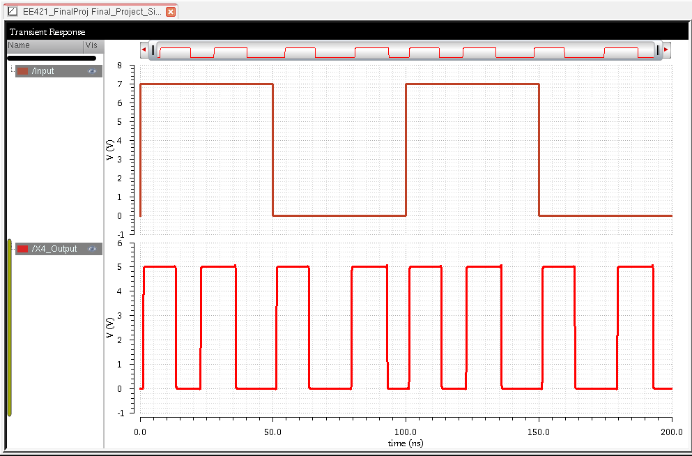
|
| Frequency, Period and VDD Values | Simulation Results |
Frequency: 11 MHz
VDD: 4V
Period: 91ns | 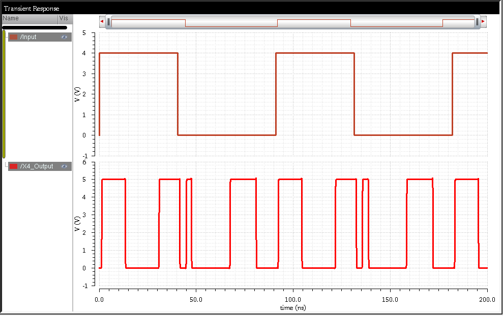 |
Frequency:11 MHz
VDD: 4.5V
Period: 91ns | 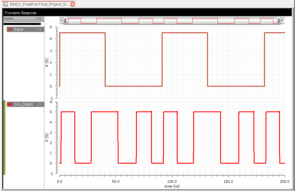 |
Frequency: 11 MHz
VDD: 5V
Period: 91ns | 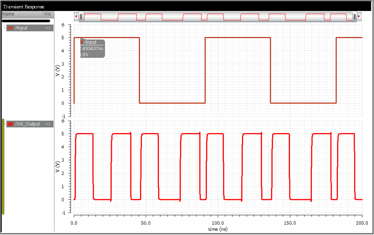 |
Frequency: 11 MHz
VDD: 5.5V
Period: 91ns | 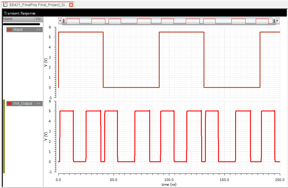 |
Frequency: 11 MHz
VDD: 6V
Period: 91ns |  |
Frequency: 11 MHz
VDD: 6.5V
Period: 91ns | 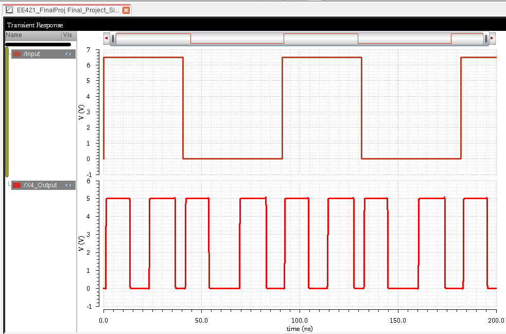 |
Frequency: 11 MHz
VDD: 7V
Period: 91ns | 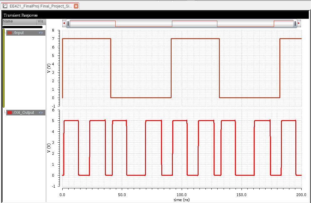 |
Final Schematic and Symbol
| Final Project Schematic | Final Project Symbol |
 | 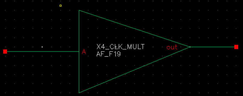 |
PART 2: LAYOUT AND DESIGN DISCUSSION
->
After verification of the schematic designs and simulations, I can now
start working on the layouts of all my buffers, XOR gate, and the final
layout of my x4 clock multiplier.
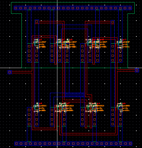
XOR GATE Layout
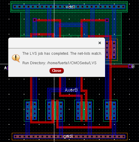
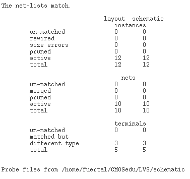
-> The XOR gate layout was already made in the previous lab, so I just used that layout for my final project.
| XOR Gate Layout View | XOR Gate Extracted View |
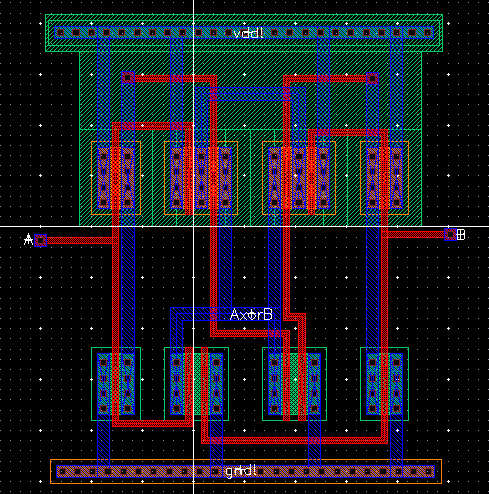 |  |
| DRC Verification |
 |
| LVS Verification | LVS Output |
 |  |
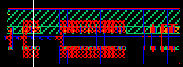
First Buffer Layout
->
For the layout of the first buffer, I referred to the buffer that I
made for HW 15, I used the same design as the homework but of course,
for the project, the sizes and multipliers would be different.
| First Buffer Layout View | First Buffer Extracted View |
 |  |
| DRC Verification |
 |
| LVS Verification | LVS Output |
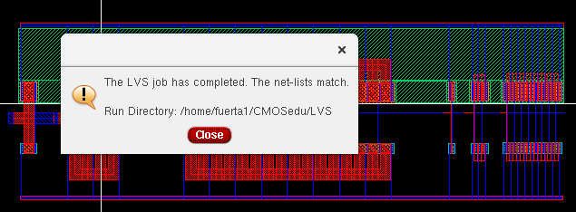 | 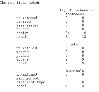 |
Small Buffer (Short-Length Buffer) Layout
| Small Buffer Layout View | Small Buffer Extracted View |
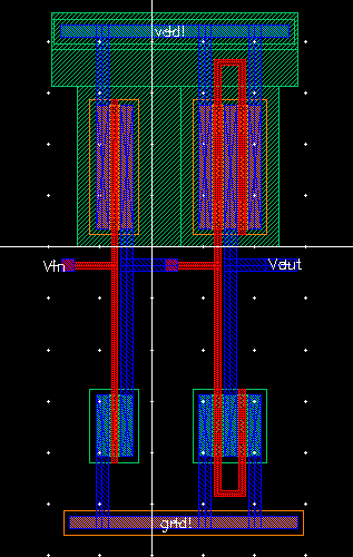 | 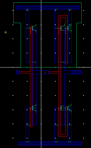 |
| DRC Verification |
 |
| LVS Verification | LVS Output |
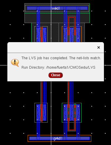 | 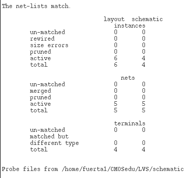 |
Second Buffer Layout
| Second Buffer Layout View | Second Buffer Extracted View |
 |  |
| DRC Verification |
 |
| LVS Verification | LVS Output |
 | 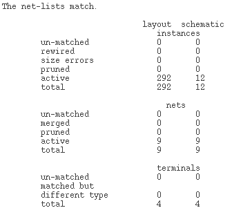 |
Final Project Layout
| Final Project Layout View | Final Project Extracted View |
 |  |
| DRC Verification |
 |
| LVS Verification | LVS Output |
 | 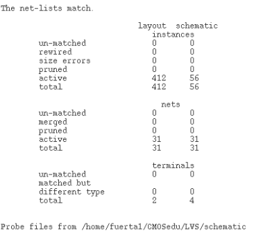 |
Design Directory: FinalProject
Return to EE421L Students
Return to My Lab Directory