Lab 3 - EE 421L
Authored
by Adrian Angelo G Fuerte
Rebelmail: fuerta1@unlv.nevada.edu
09/17/2019
Pre-Lab
For the pre-lab of this laboratory, we
were tasked to back-up all of our previous work from the lab and the
course. After doing that, we were to finish the rest of tutorial one,
which was to create a schematic, symbol and a layout for the voltage
divider and run an LVS check.
Schematic
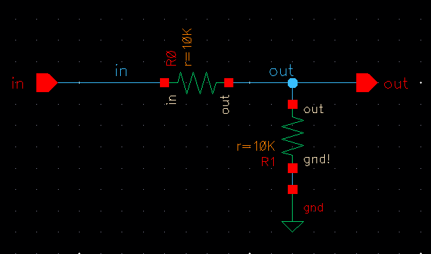
Symbol
Layout
Netlist Result
Lab
description
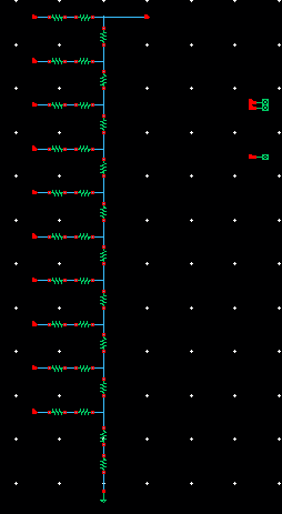
For this lab, I
copied my designed 10-bit DAC from lab 2 and using the n-well to layout
a 10k resistor (shown in tutorial 1), we use that n-well resistor in
the layout of our DAC and verify with LVS that their netlist match.
The
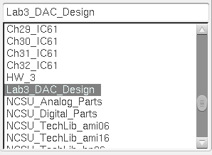
first step that I did for this lab is that I created a new library for
lab 3 and called it "Lab3_DAC_Design" and I copied my DAC schematic and
simulations from lab 2 onto my new library. Then I set-up a new layout
design from my lab 3 library by selecting File-->New-->Cellview
Created New Library
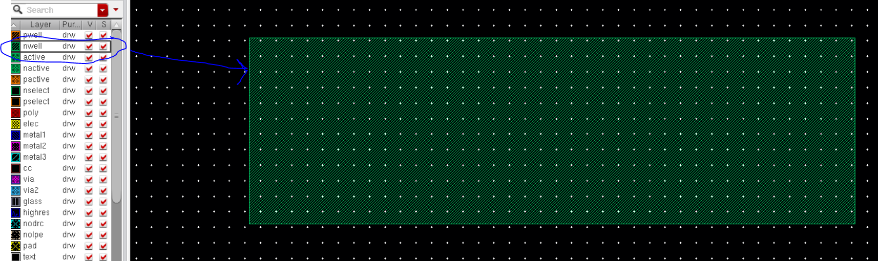
After creating
a new layout, I began making the resistor and the n-well layer. This
was done by selecting n-well on the left side and press R and then
drawing a rectangular box. At this point the n-well layer is not yet
defined as a resistor and its dimensions are not yet defined. In order
to determine the dimensions of the N-well and determine its length and
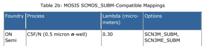
width, we have to refer to MOSIS. In the C5 process, lambda =
0.30um, the minimum size of the width of the n-well is 3.6 microns. To
calculate the length and the width of the n-well resistor, the
following equation can be used: R = (roh/t)*(L/W). Where the value of roh/t is the sheet resistance, which in C5 process is approximately 800 microns, t
is the thickness which is neglected because we cannot control how thick
the n-well is on Cadence. The only variables that we can control is the
L (length) and W(width) of an n-well. Given that the minimum width of
an n-well is 3.6microns, we can solve for the length given that we have
the resistance, sheet resistance and width. For this lab I used 6
microns for width and calculated a value of 75 microns for length.
MOSIS
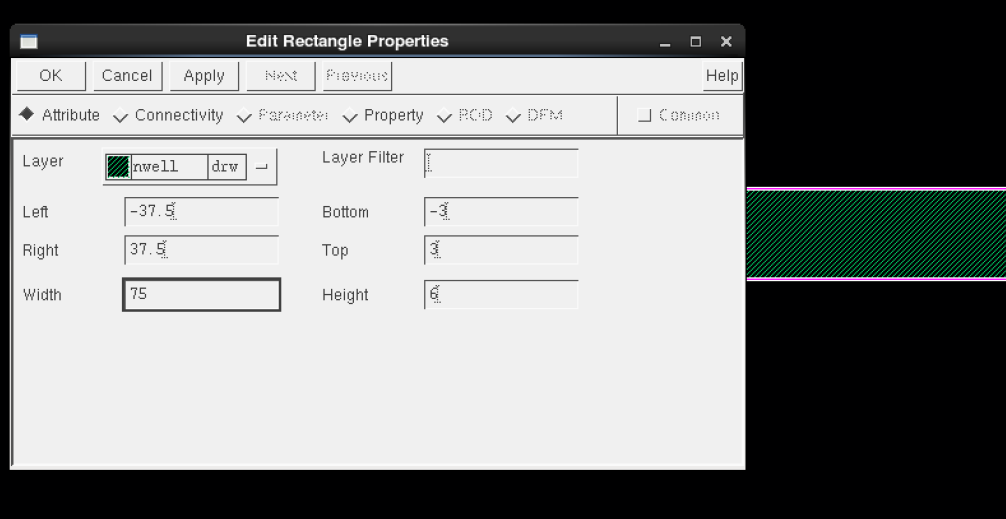
Drawing N-well
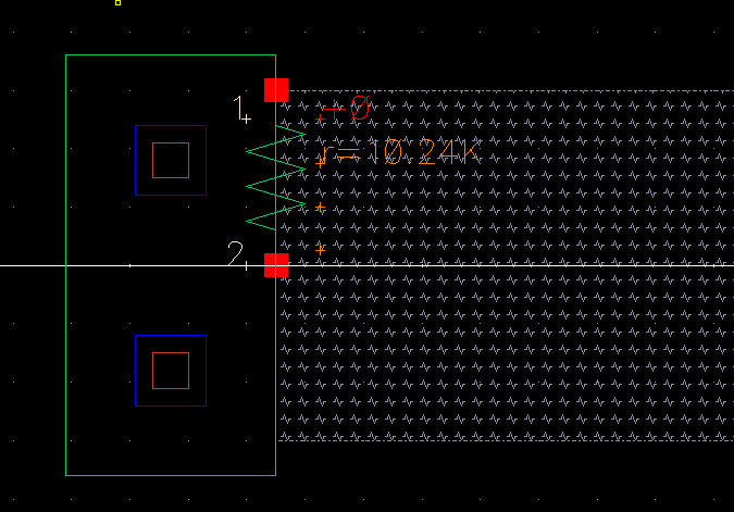
Entering dimensions of N-well: Select N-well layer ---> press Q
After
I inputted the values for the length and width of the n-well, I went
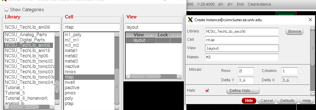
ahead and added the "ntap" object which is used as a slot on both sides
of the n-well resistor so that the other resistors can be connected to
it. Make sure to use ntap
(lowercase). This is done by pressing the instance key "I" and browsing
to "NCSU_Techlib_ami06" library. I used 2 rows and 1 column for
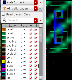
my ntap. After doing so, I used the metal 1 layer to connect the two
slots of the ntap on both sides of the resistor. Then I pressed
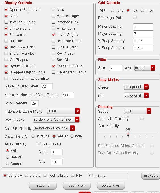
"E" to bring out the display controls and made sure to check "Pin
Names" to shows pin labels and set stop to 10. Then I applied "res_id"
over the body of my n-well resistor and extracted the layout of my 10k
resistor to verify that it is indeed 10k.
Adding ntap
Added ntap and connected using metal 1 layer
Display Options
Added res_id
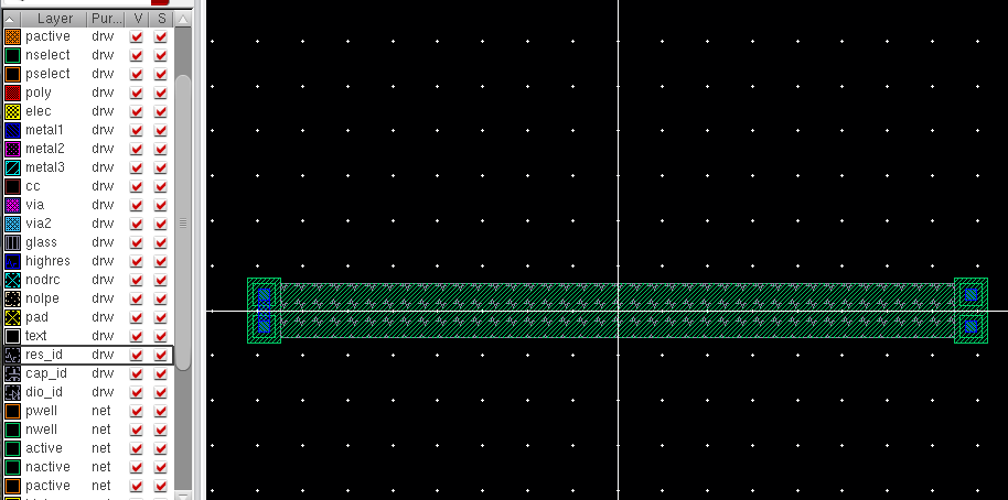
Result of my layout
Extracted and Verified
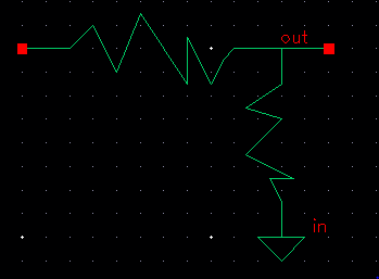
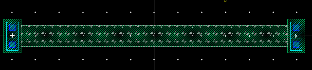
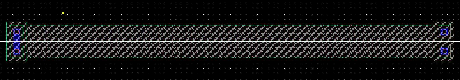
The
next step that I did is to create a layout for three 10k n-well
resistor that resembles a portion of my DAC and I will be using to
instantiate my final 10-bit DAC. To make sure that my schematic of
three 10k resistors match the layout, I LVS'd it and got a netlist match
Three 10k resistor schematic
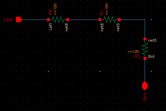
Layout
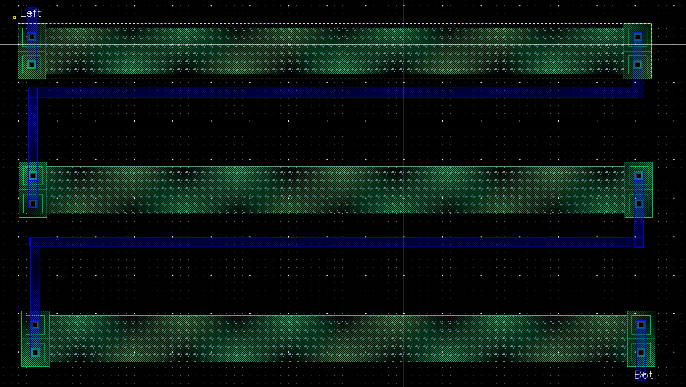
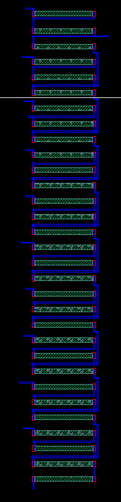
The
next step that I did is to make a full layout of my 10-bit DAC, in
order to do that I used my layout from the image above and before
instantiating it, I removed the labeled pins (Left and Bot) and
replaced it with labels from B9:0 (B9 to B0) to match the labels on my
10-bit DAC schematic. I made sure to stack the layout design (same X
position different Y position). Shown below are the images of my 10-bit
DAC layout instantiated with 10k resistors.
Full View (schematic before instantiation)
Full View (After Instantiation)
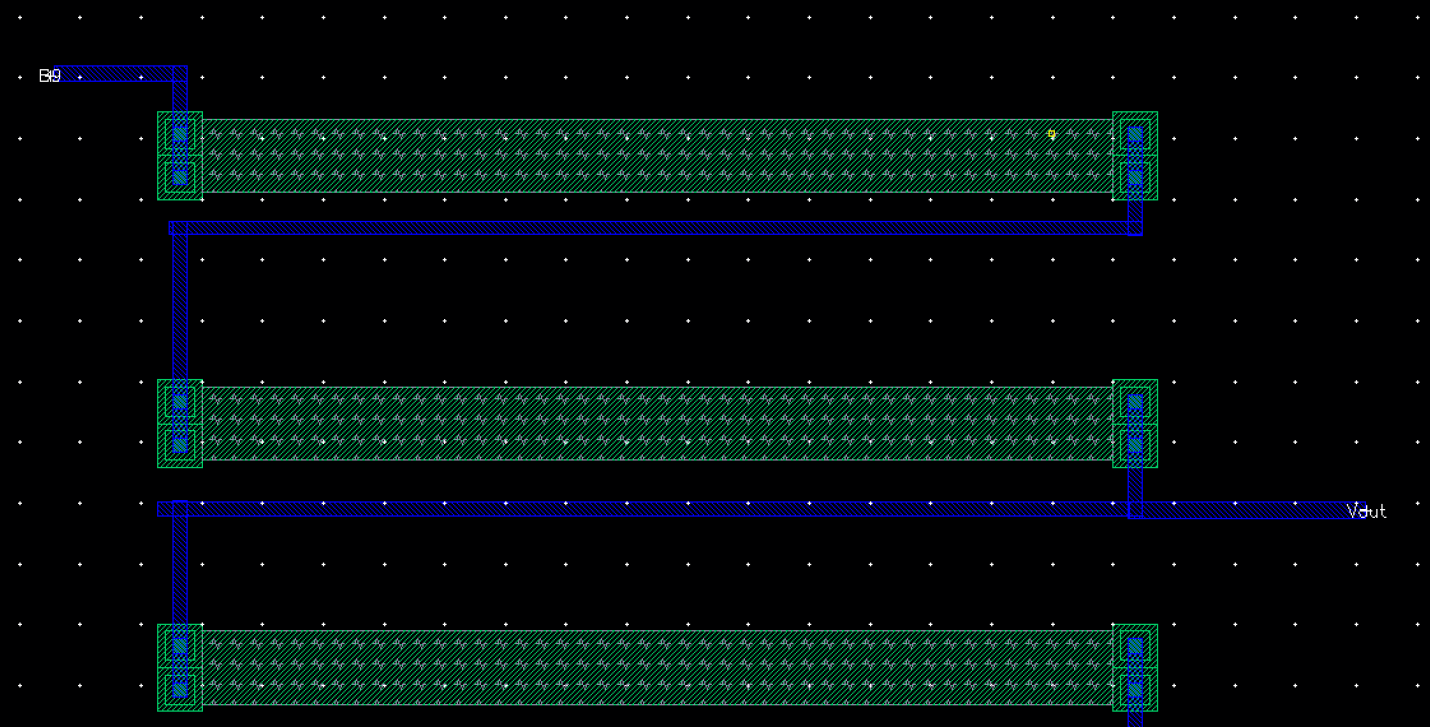
Top (Showing B:9 and Vout)
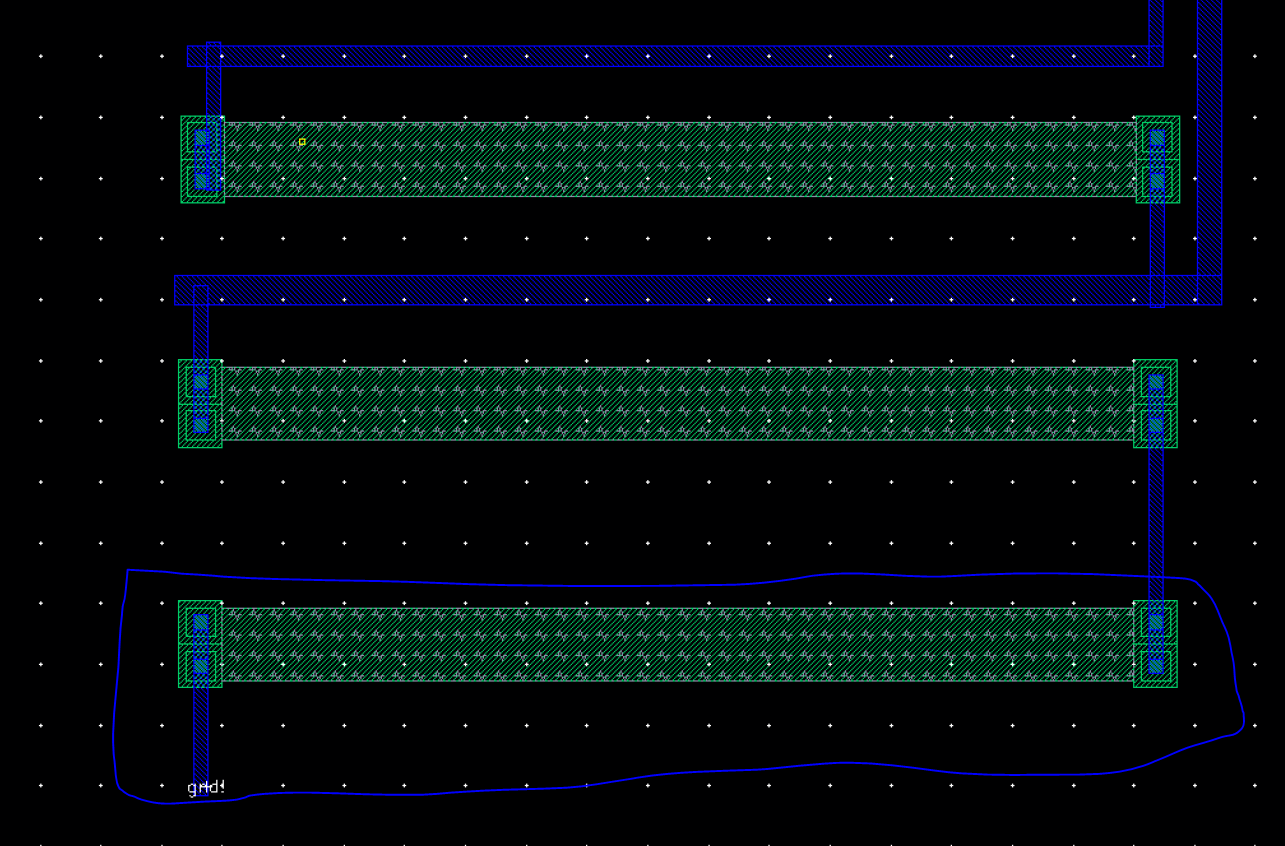
Bottom View (Added another 10k resistor before ground to fulfill the 2 10k resistor from the schematic)
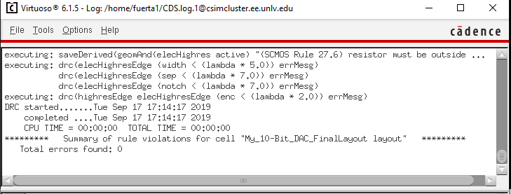
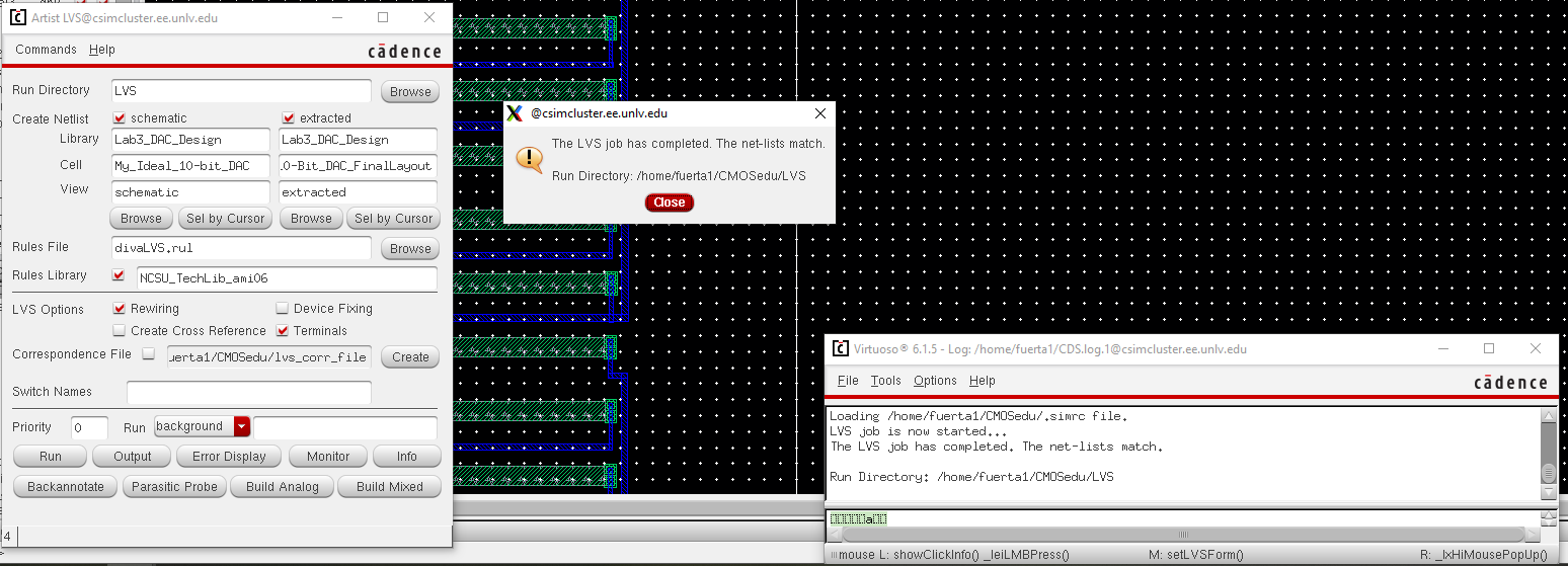
After
finishing the layout, I DRC'd my 10-bit DAC and LVS'd it to make sure
that there were no errors and that the netlist matches. To do the DRC,
click Verify --> DRC.
To
do LVS, click Verify --> LVS ---> browse schematic (put your
schematic design) ----> browse extracted (put your extracted layout)
---> Run
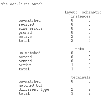
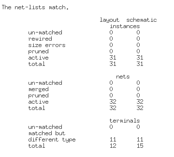
To
get the output result, after running LVS a window will open stating
that the net-lists match, close that windown and then on the LVS window
click Output
DRC Result
Netlist Match
Output Result
Click here to go to my final design folder of DAC: Lab3_DAC_Design.zip
Return to EE421L Students
Return to My Lab Directory