Lab 2 - EE 421L
Authored
by Adrian Angelo G Fuerte
Rebelmail: fuerta1@unlv.nevada.edu
09/11/2019
Pre-Lab
Part 1
For
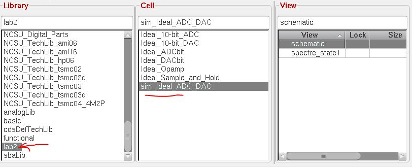
the pre-lab I was tasked to upload and unzip the given lab 2 file from
CMOSedu website onto my CMOSedu directory via MobaXterm. The lab 2 file
contains simulation examples using an ideal 10-bit Analog-to-Digital
Converter (ADC) and Digital-to-Analog Converter (DAC). It also contains
the schematics for both converters that are going to be used for
simulations. After uploading and unzipping the file, I had to define
this file in the cds.lib in my CMOSedu directory to be able to use and
simulate the schematics that were provided.
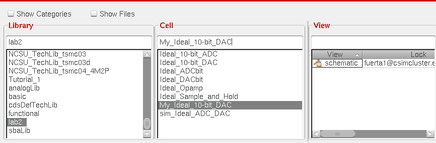
Lab 2 File
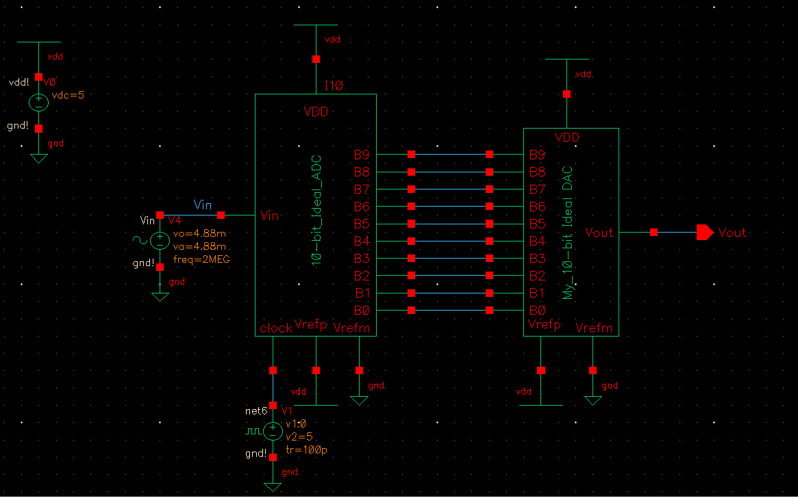
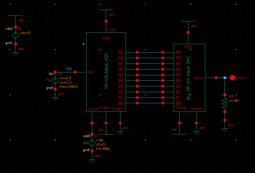
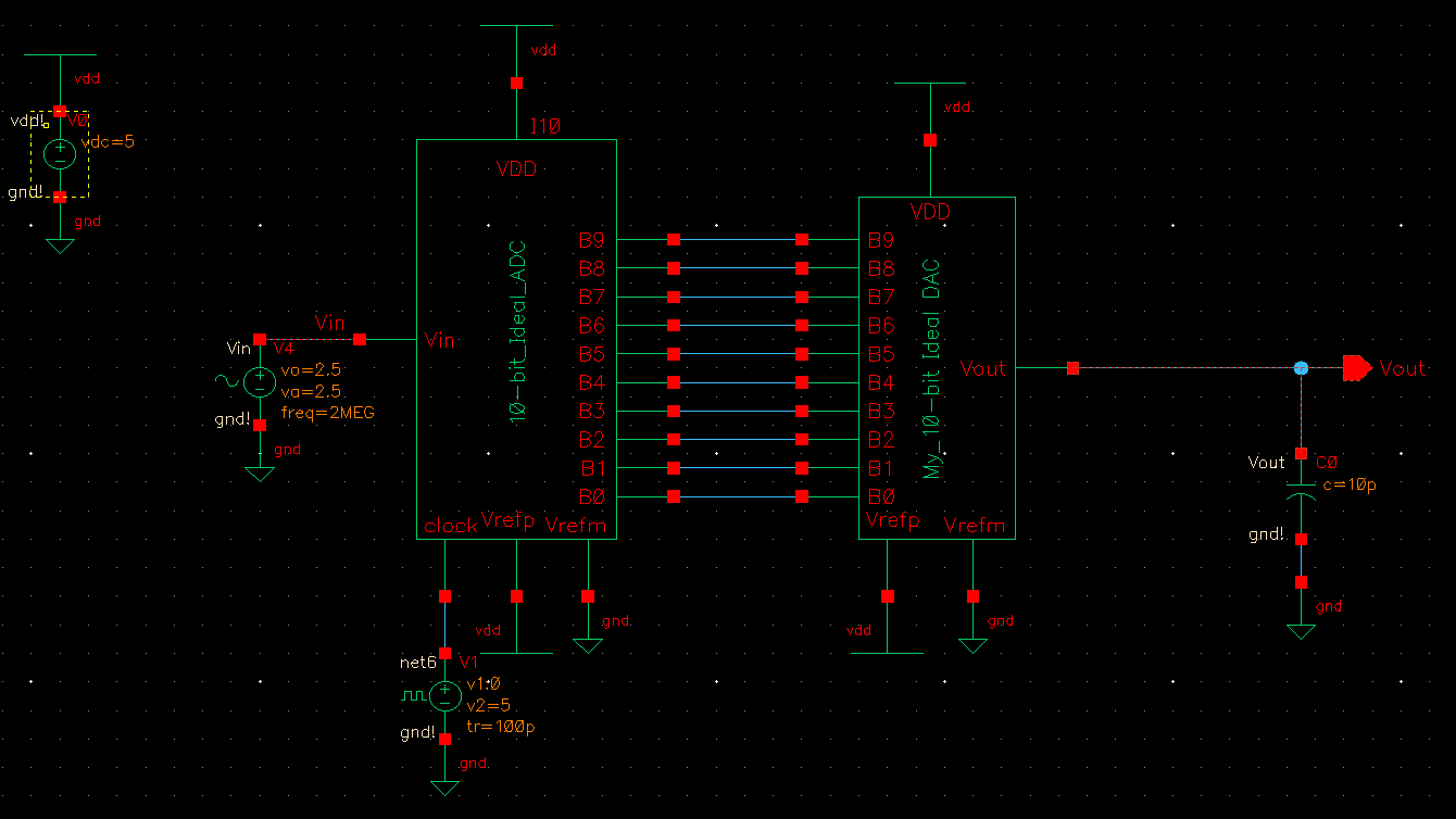
Top-Layer Schematic (Ideal ADC_DAC Schematic)
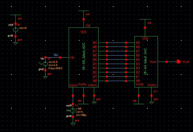
After
opening the schematic (shown above), we then started the simulation by
selecting Launch --> ADE L which takes us to the editor window and
once there, select Session --> Load State --> OK which triggers
the simulation and gives us the transient response values of both Vin
and Vout shown below. I then proceeded to change the background to
white and changed the plot lines from dashed to silid line in order to
have a clearer view of the waveforms generated.
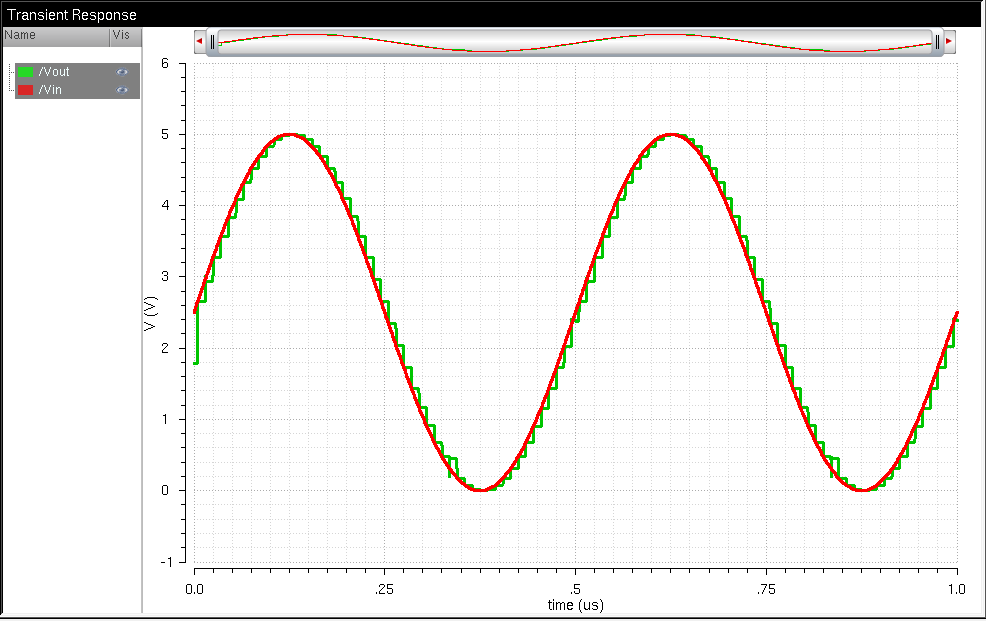
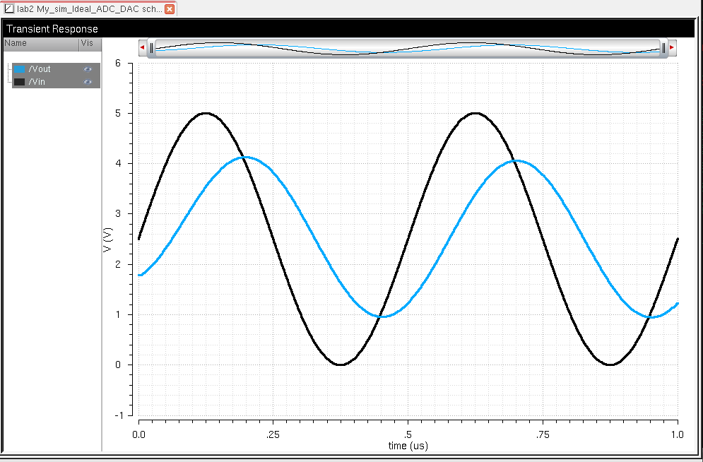
Simulation
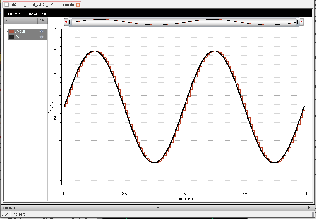
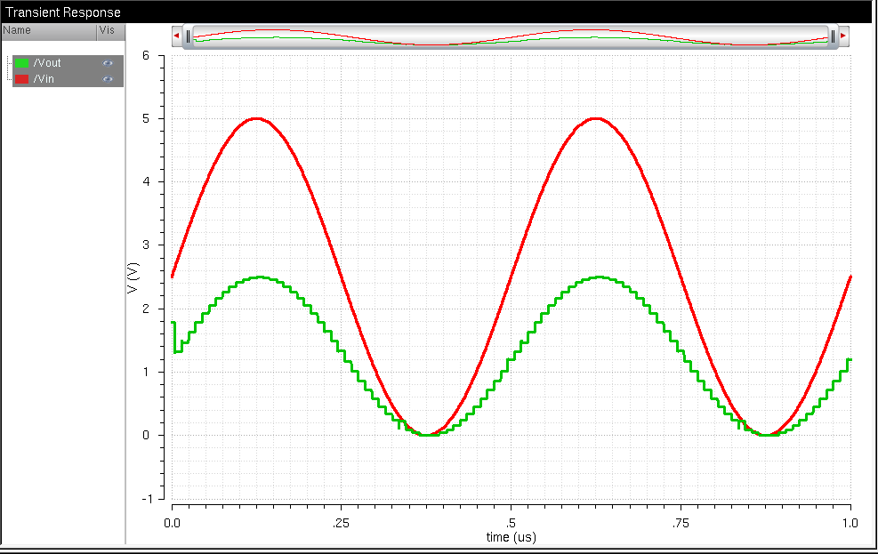
The
simulation result shows that the relationship between Vin and B[9:0] is
that the ADC takes the input from the Vin and converts this input into
a digital signal that produces a 10 bit binary value. This 10 bit
binary value is then recieved by the DAC which then outputs an analog
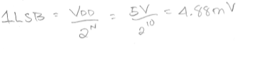
signal Vout. In order to determine the least significant bit (LSB) we
simply use the equation shown below where we plug in our VDD and N. By
doing this we get the value of Vout to be 4.88mV which represents the
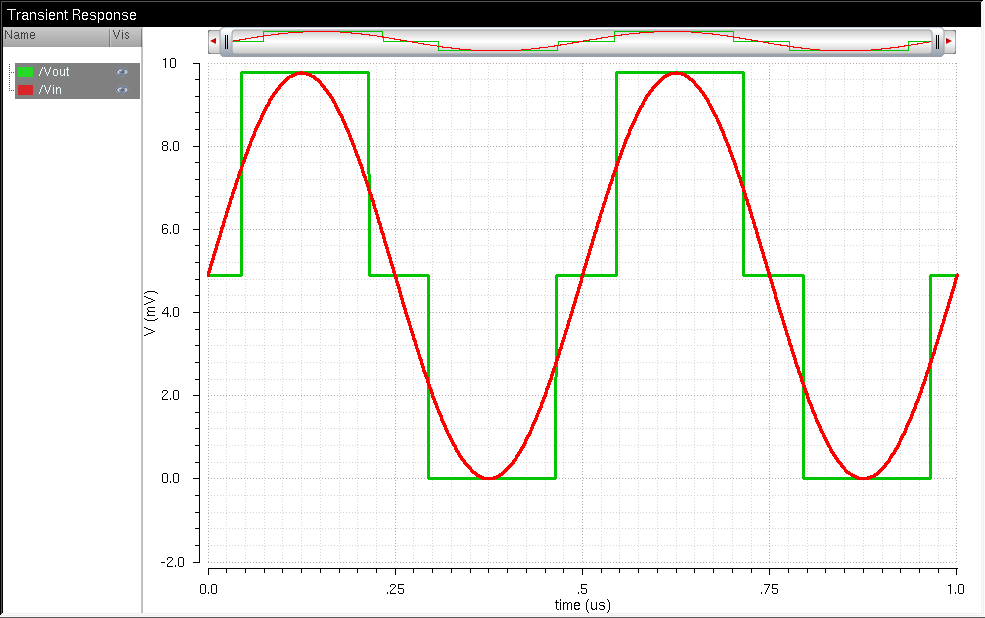
least significant bit at 0000000001. The graph below shows Vout when the amplitude and offset is at exactly 4.88mV
LSB Calculation

Graph
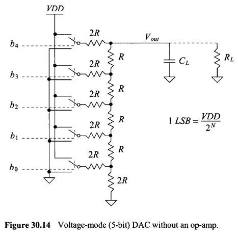
Laboratory Description
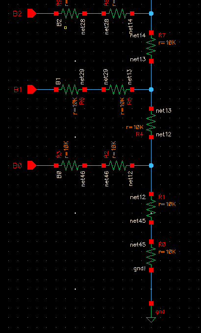
In
this laboratory we will be using n-well resistors to implement a 10-bit
DAC. Our design is based on the topology in figure 30.14 from the CMOS
book. The schematic that we are going to be replacing the original DAC
schematic with is seen in the image below.
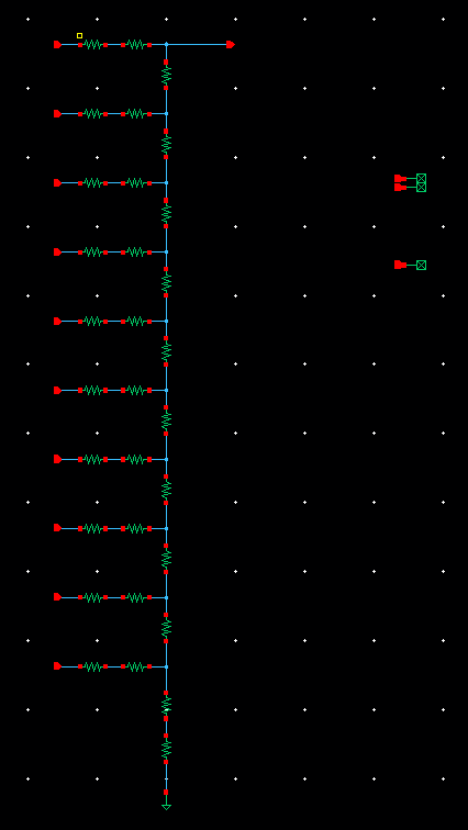
Part 1
The
first thing that I did is to copy the ideal 10-bit DAC schematic that
is already in my library and rename it into "My_ideal_10bit_DAC". I
then opened My_ideal_10-bit_DAC and transformed the original DAC
schematic with the new DAC schematic from figure 30.14.
Original DAC schematic
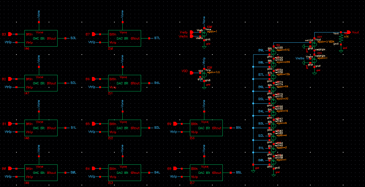
My Schematic
Part 2
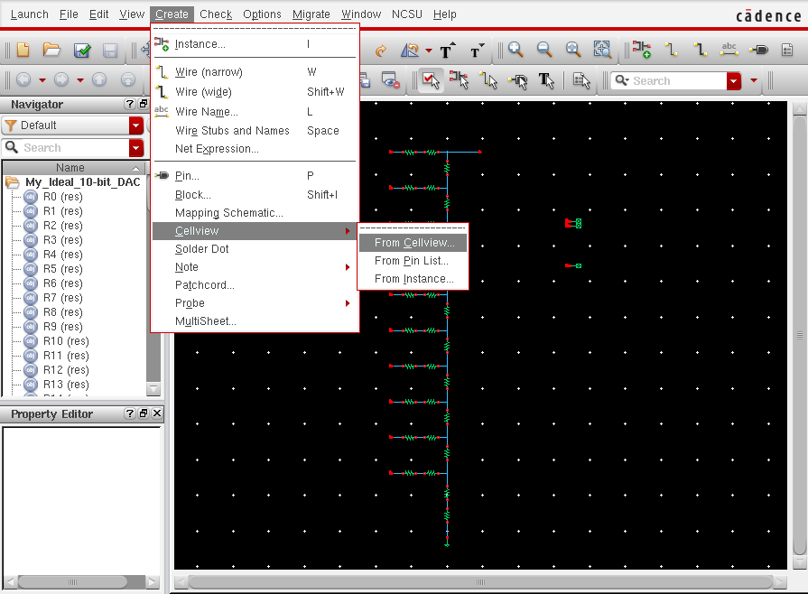
After
transforming the old DAC to my DAC, I then proceeded to create a symbol
using my schematic with the exact same footprint as the
Ideal_10-bit_DAC. This was done by going to Create --> Cellview
--> From Cellview and a new window will appear, make sure that on
the tab that says "From View Name" select symbol. You could also just
re-use the symbol from the Ideal_10-bit_DAC by copying it to your
10-bit DAC schematic. After this process, I editted my symbol and named
it "My_10-bit_Ideal DAC". I also made sure that the vrefp, vrefm, and
vdd pins are connected with "noConns".
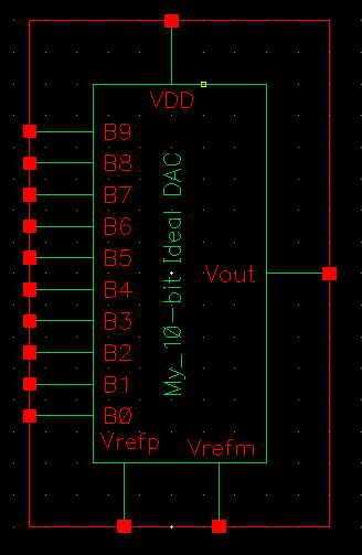
My Symbol
Part 3
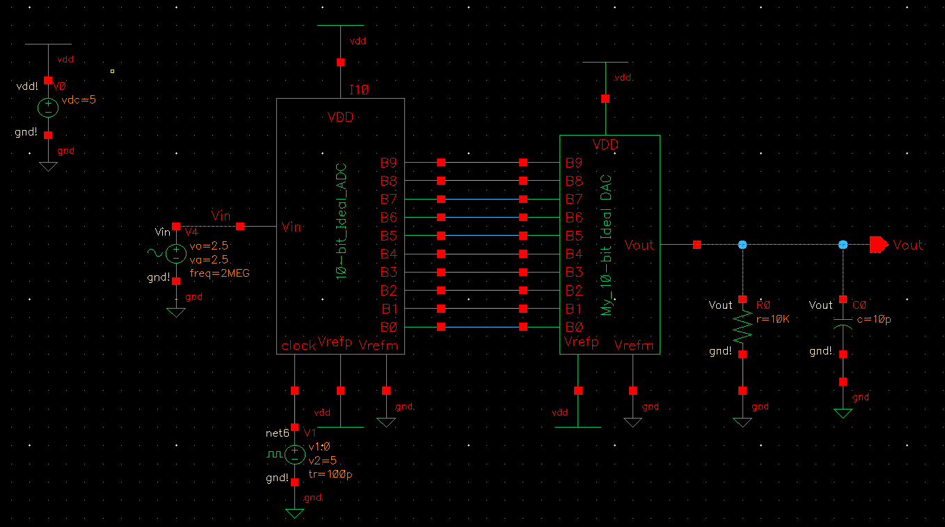
After
creating my symbol, I then proceeded to copy the cell sim_Ideal_ADC_DAC
and renamed it to My_sim_Ideal_ADC_DAC and replaced the 10-bit ideal
DAC symbol with the one that I made, shown in the image below. I then
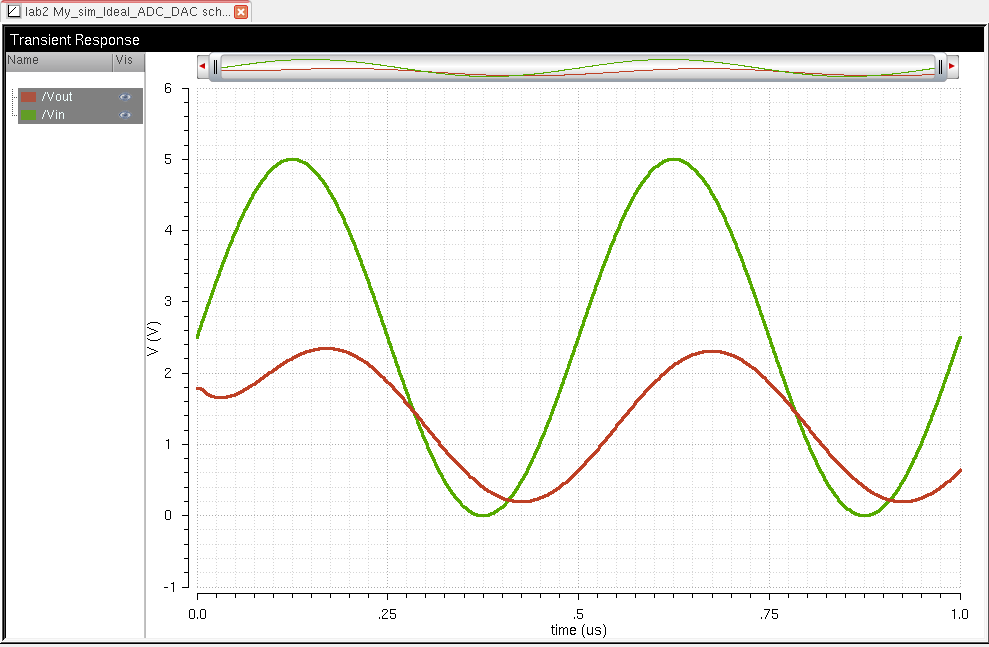
proceeded to simulate and got the following result.
Simulation Result
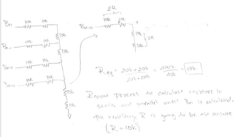
Hand Calculations
LSB Hand Calculation
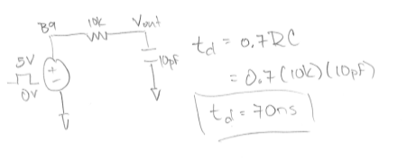
Delay, Driving Load Hand Calculation
Output Resistance of DAC Calculation
Part 4
I
then performed different experiments to my design to see what happens
when I ground all DAC inputs except for B9 and connect B9 to a pulse
source from 0 to 5V (0to VDD). I also simulated to see what would
happen if my DAC drives a load (resistor, capacitor, and both resistor
and capacitor). The results are shown in the images below
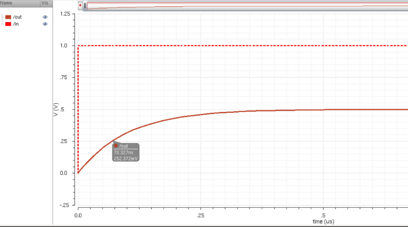
Ground all inputs except for B9
Grounding
all inputs except for B9 and connecting B9 to a pulse source, proves my
hand calculation that the time delay of the DAC is 0.7RC which is about
70ns.
Resistor Load (Schematic and Simulation)
As the simulation shows, driving a 10k resistor to the output, halves the magnitude of the input voltage.
Capacitive Load (Schematic and Simulation)
Adding
a 10pF capacitive load to the output is a smooth sinusoidal curve but
it delays the output voltage. This is lagging the output voltage
by about 70ns
Resistive Load and Capacitive Load (Schematic and Simulation)
By
adding both a 10k resistor and 10pF capacitor to Vout, the input
voltage is cut to about half and we get a smooth sinusoidal curve and
delays the output by about 50ns
Discussion (What happens if the resistance of the switches isn't small compared to R)
In
a real circuit, if the resistance of the switches isn't small compared
to R, then the resulting output resistance is going to be higher. The
output voltage will decrease significantly because of the higher
resistance.
The bigger the R, the smaller the output voltage will become.
Return to Lab Directory
Return to Students Directory