Project - ECE 421L
Email Address: cortej2@unlv.nevada.edu
Lab Date: Nov 13, 2019
--------------------------------------------------------------------------------------------------------------------------------------------------------------------------------------------------------------------------------------------------------------
--------------------------------------------------------------------------------------------------------------------------------------------------------------------------------------------------------------------------------------------------------------
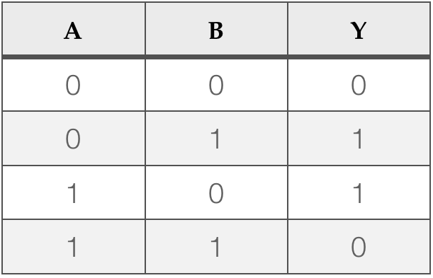
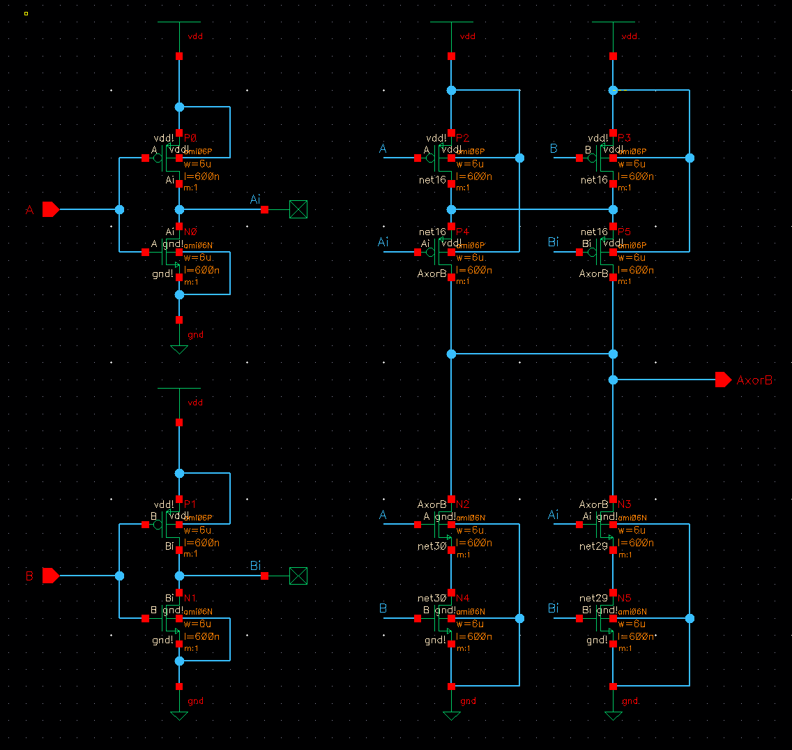
Purpose of XOR gates:
The XOR truth table is shown below.
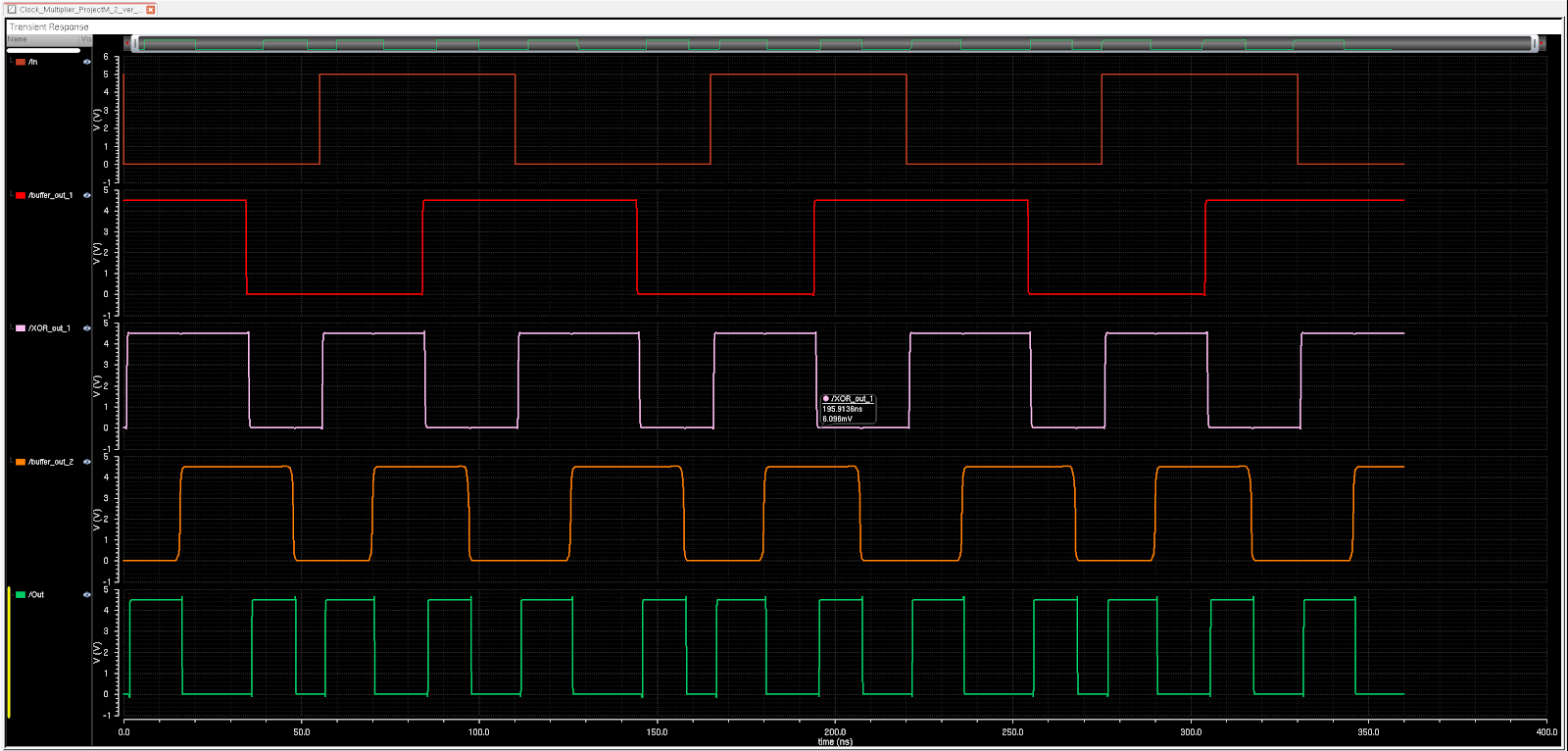
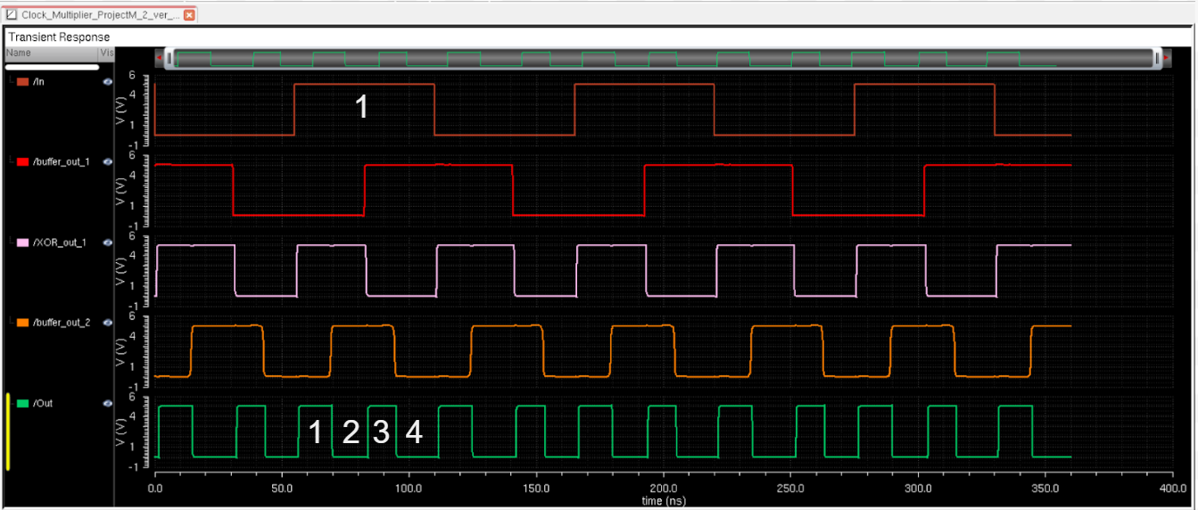
The
XOR gate produces a x2 signal because of the way it is taking in it’s
two signals. Both signals originate from the same source, but one
of them is
delayed
due to the buffer. This delay allows the input and output to be:
00->0, 10->1, 11->0, 01->1. This pattern is repeated and
appears as the x2 signal.
The same XOR gate was used for both stages.
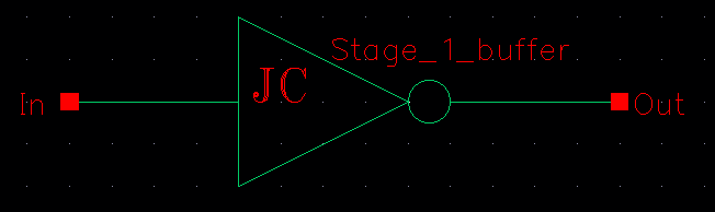
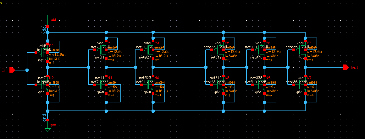
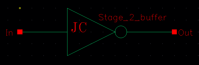
Purpose for the buffers:
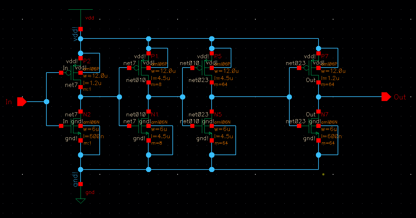
The buffers for the first and second stage are different to perform appropriate delays given the frequency.
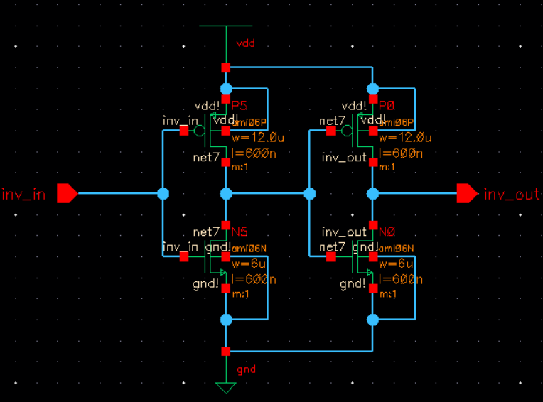
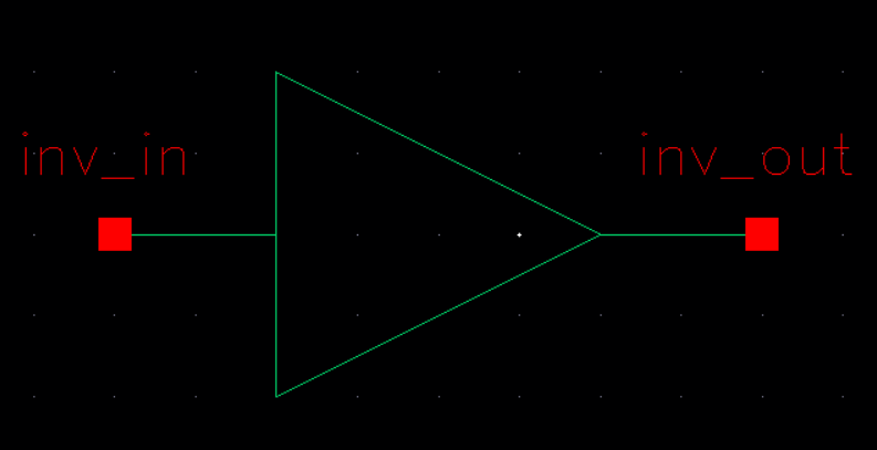
Below is the symbol and schematic for the stage 1 buffer.
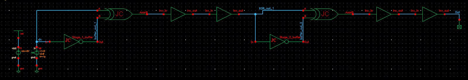
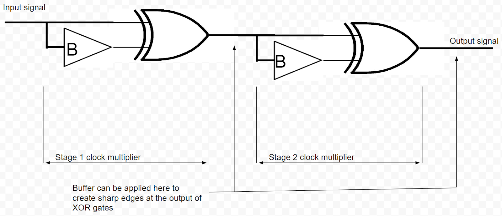
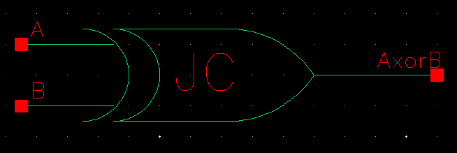
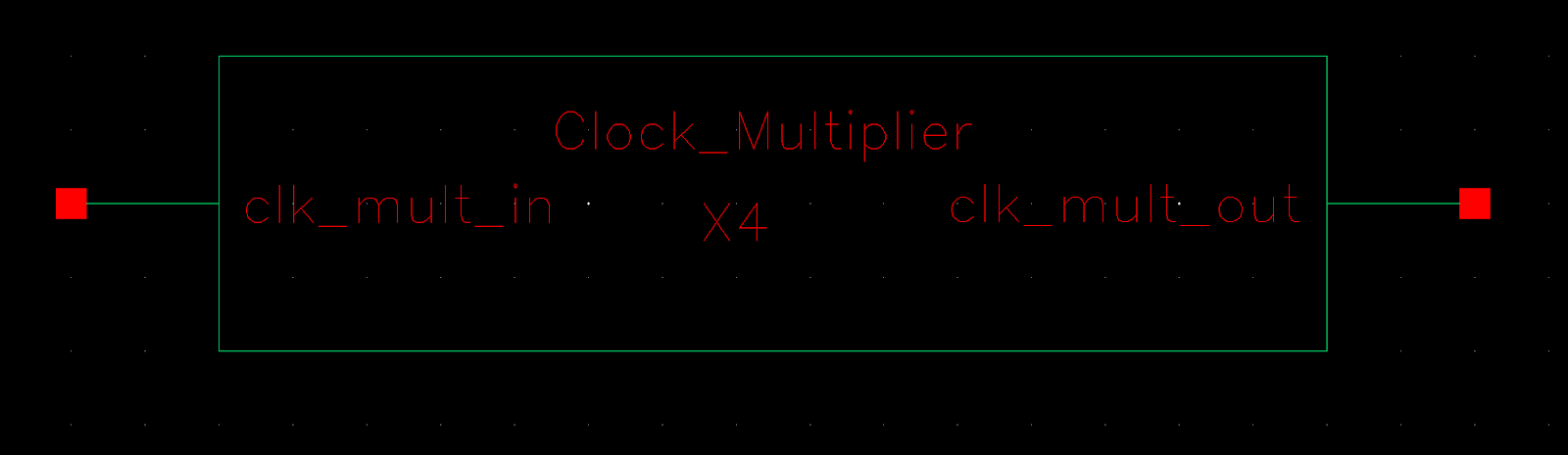
The symbol for the clock multiplier is shown below.
Tests:
change in VDD
Test conditions freq=9.09 MHz, VDD= 4 V | 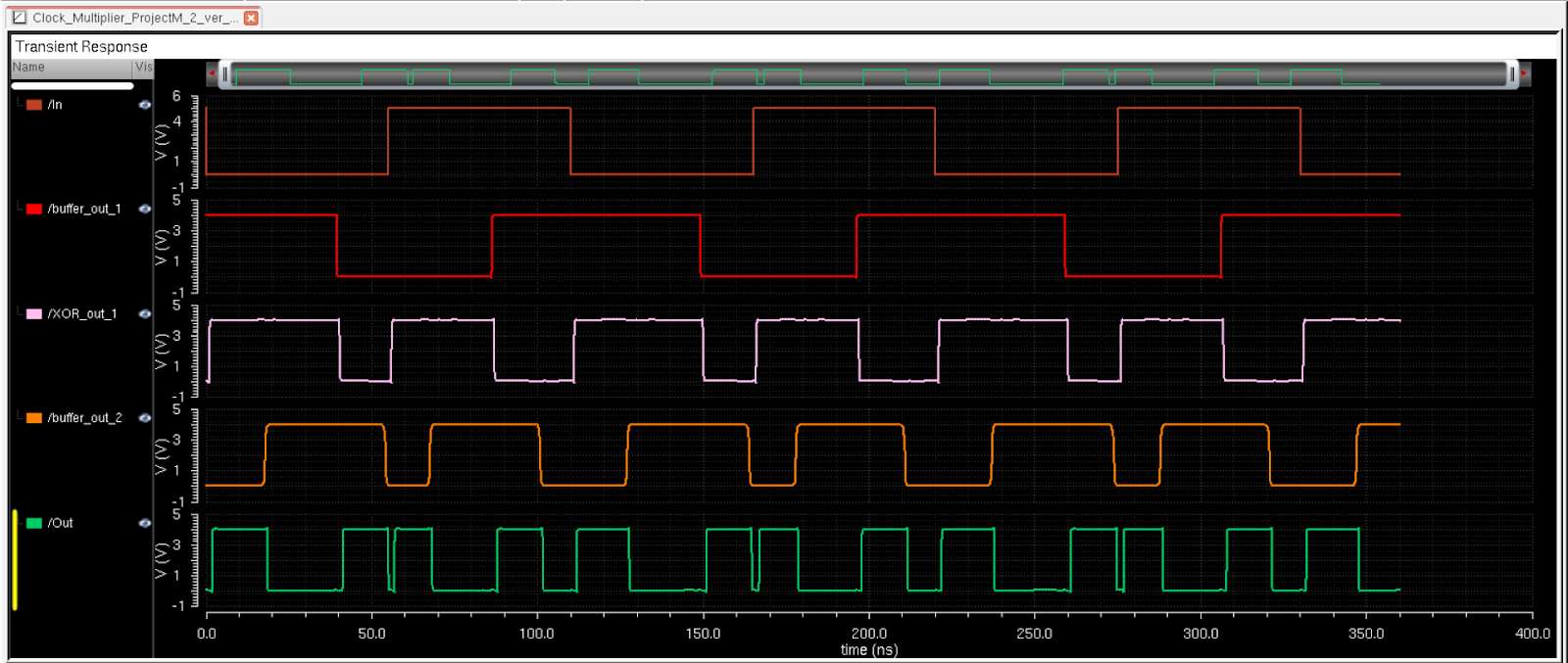 |
Test conditions freq=9.09 MHz, VDD= 4.5 V |
|
Test conditions freq=9.09 MHz, VDD= 5.5 V | 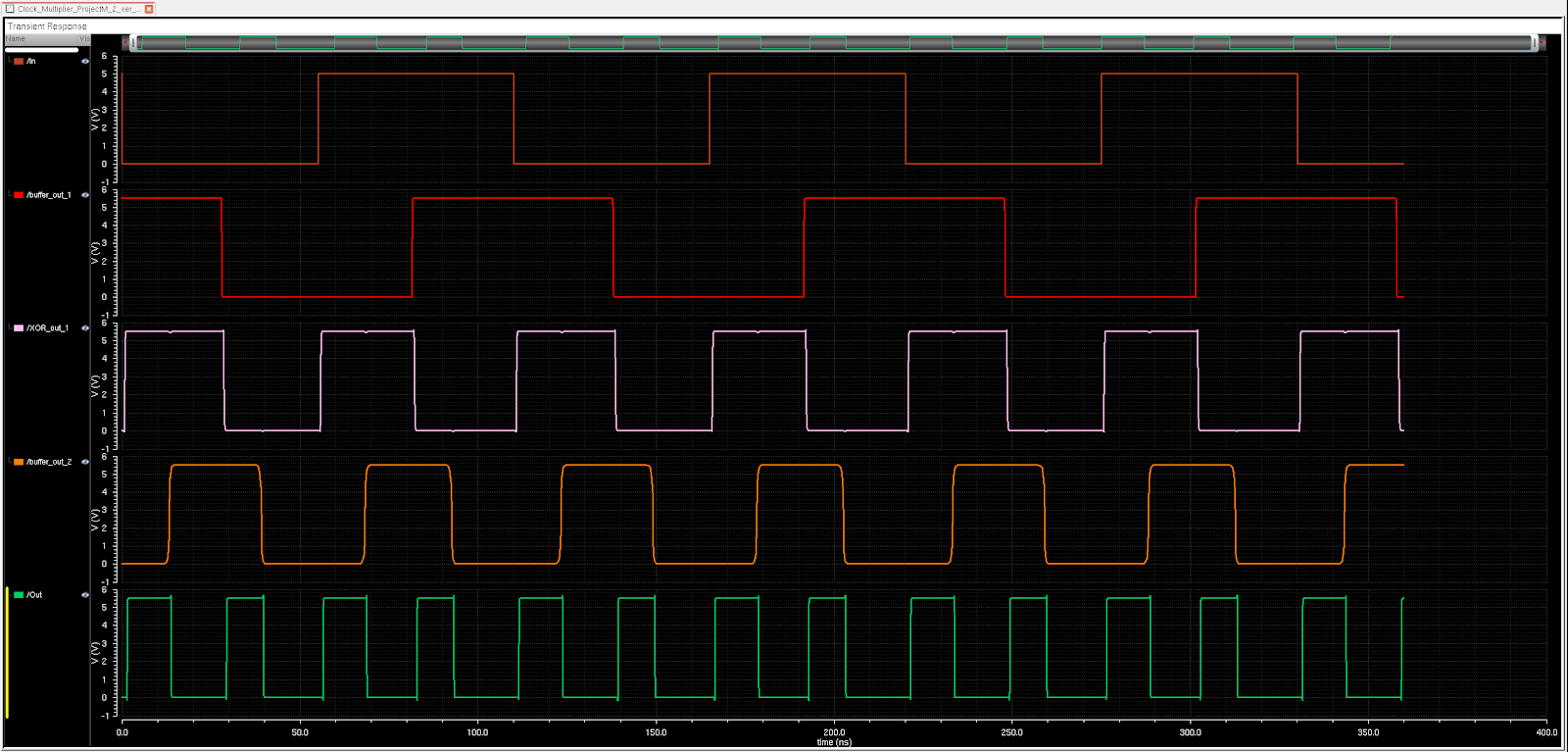 |
Test conditions freq=9.09 MHz, VDD= 6 V | 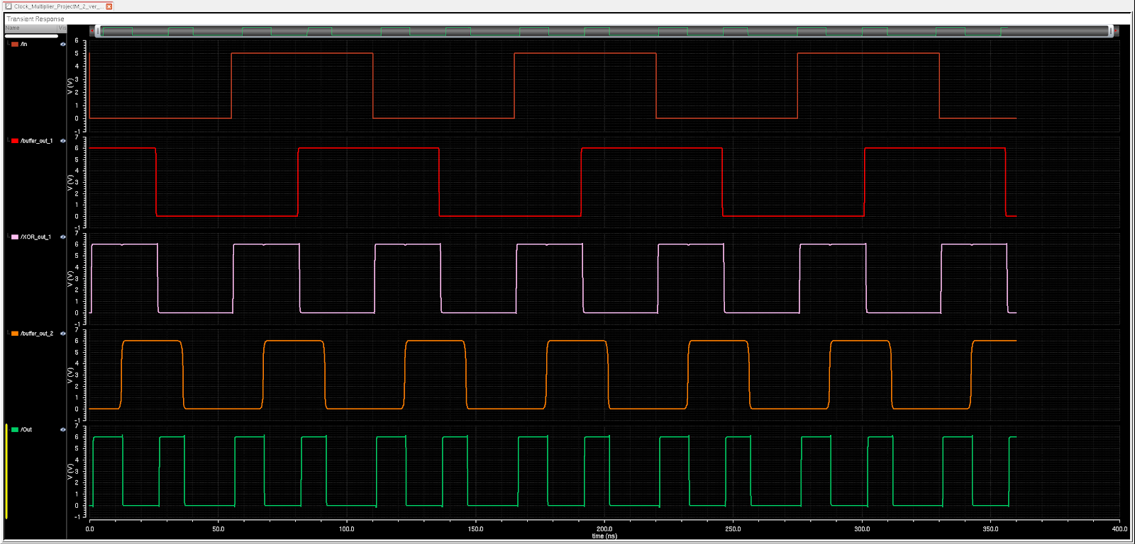 |
Tests:
change in frequency
Test conditions freq=7 MHz, VDD= 5 V Period of voltage source is 140 ns | 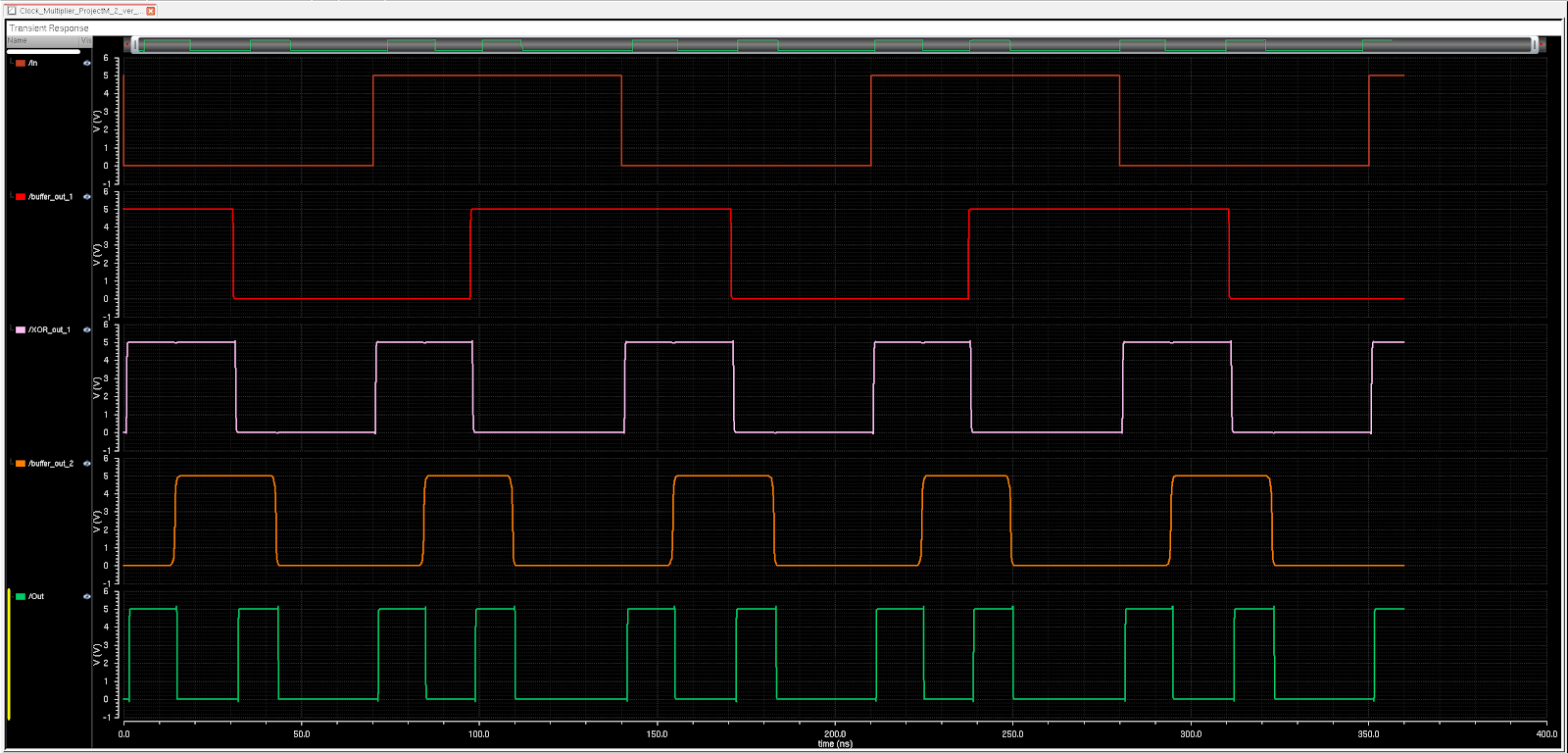 |
Test conditions freq=8 MHz, VDD= 5 V Period of voltage source is 125 ns | 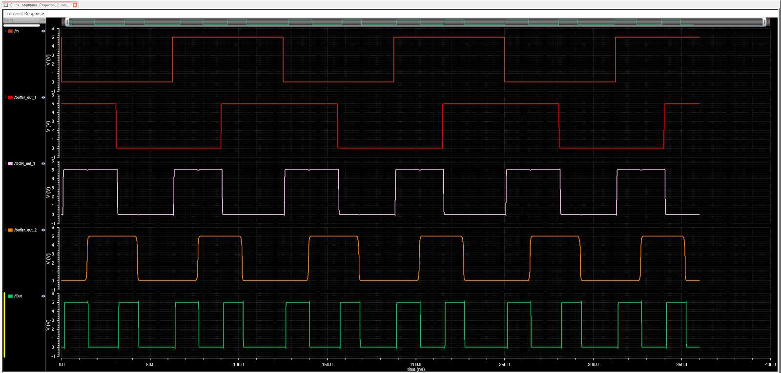 |
Test conditions freq=10 MHz, VDD= 5 V Period of voltage source is 100 ns | 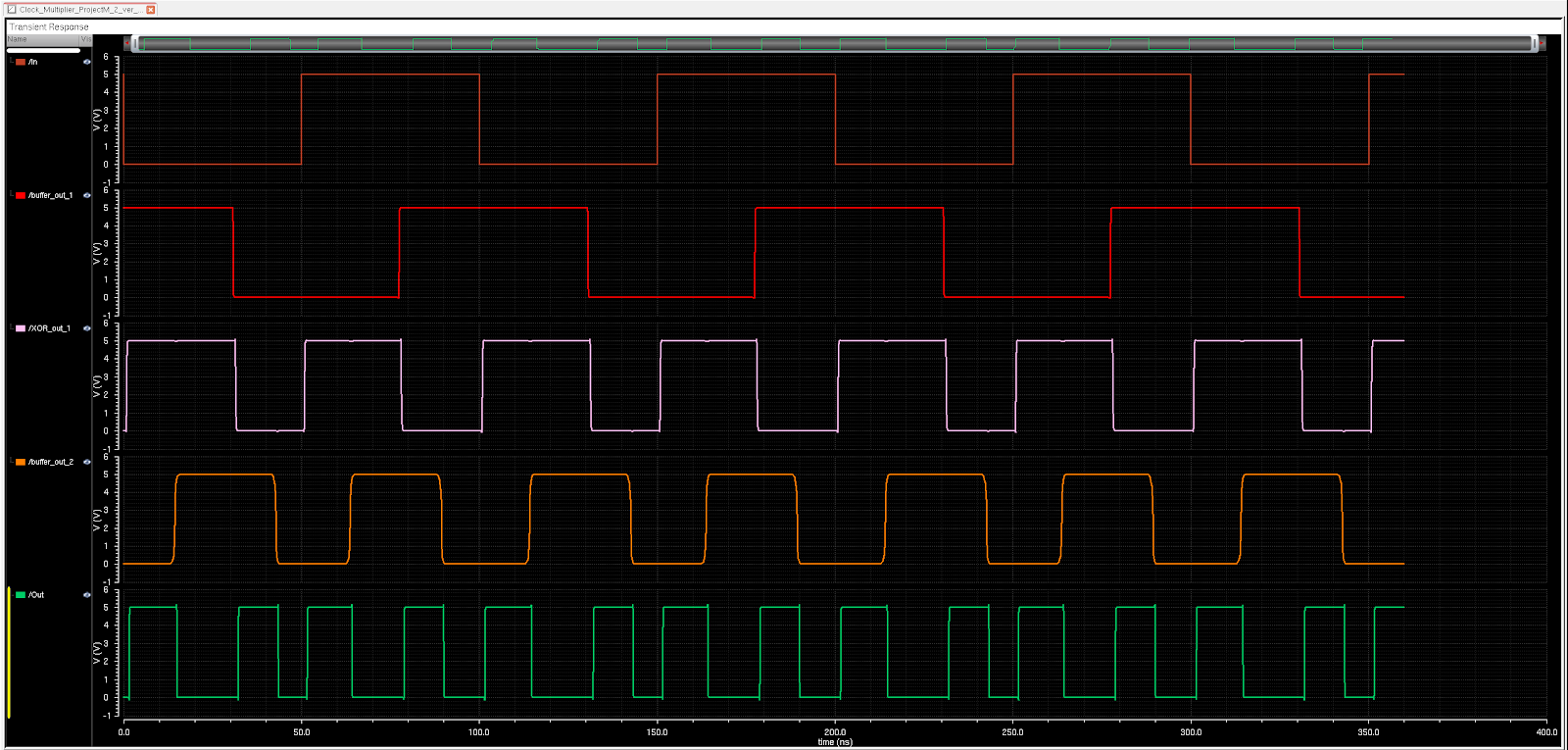 |
Test conditions freq=11 MHz, VDD= 5 V Period of voltage source is 90.9 ns | 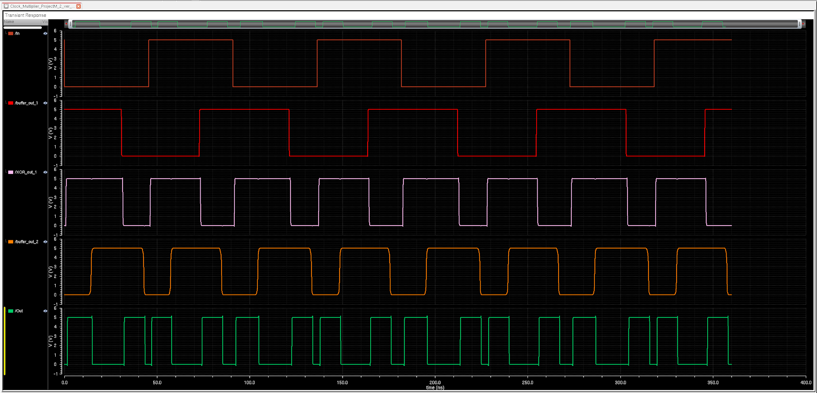 |
Test conditions freq=12 MHz, VDD= 5 V Period of voltage source is 83.3 ns | 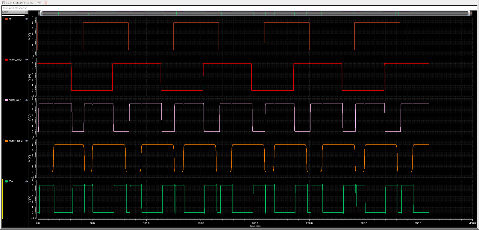 |
Test conditions freq=13 MHz, VDD= 76.9 V Period of voltage source is 140 ns | 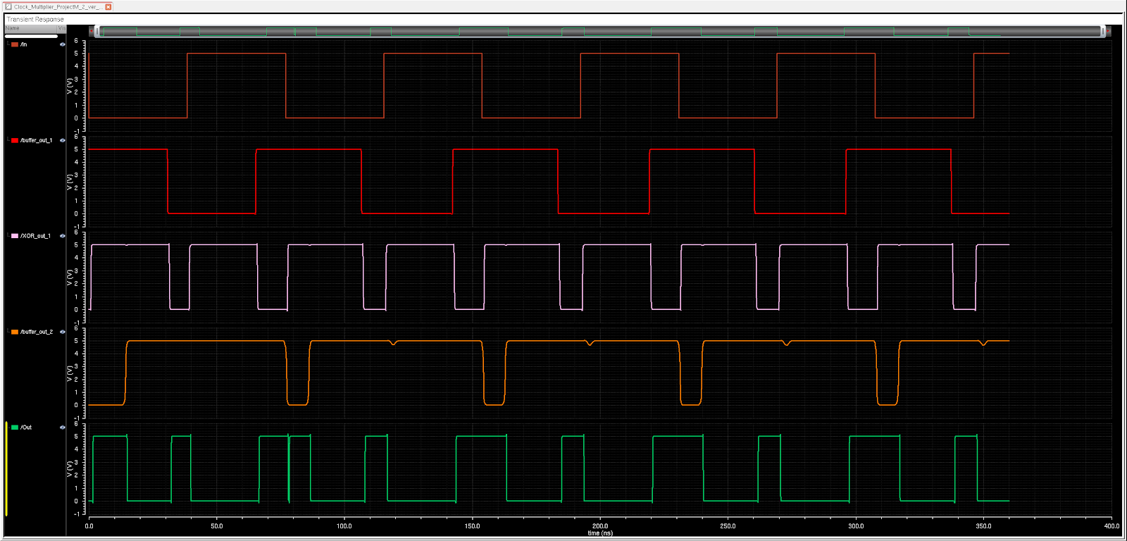 |
--------------------------------------------------------------------------------------------------------------------------------------------------------------------------------------------------------------------------------------------------------------
Project Part 2:
Below is the layout for the first stage buffer used in the clock multiplier, as well as other relevant screenshots.
| Symbol | 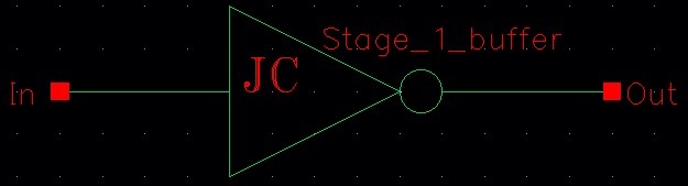 |
| Layout | 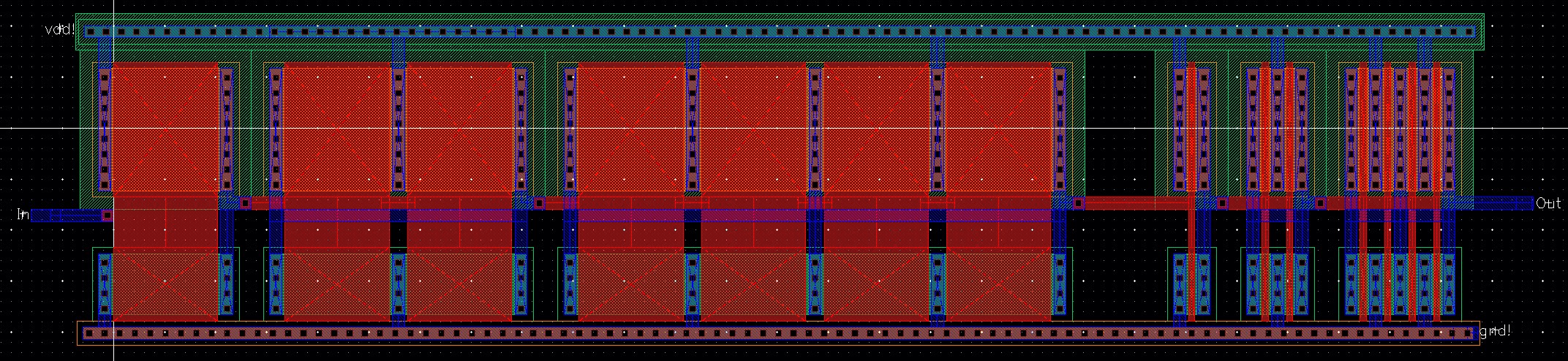 |
| DRC | 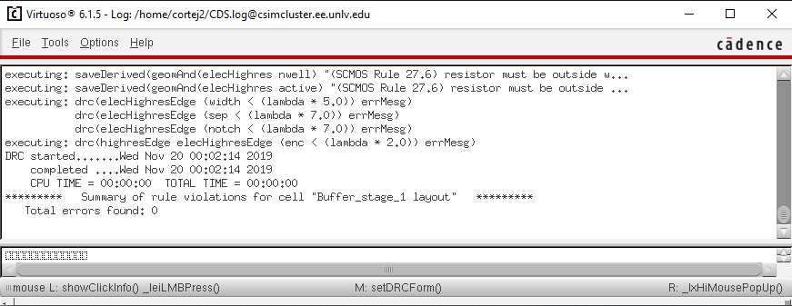 |
| LVS | 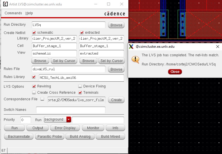 |
Below is the layout for the second stage buffer used in the clock multiplier, as well as other relevant screenshots.
| Symbol | 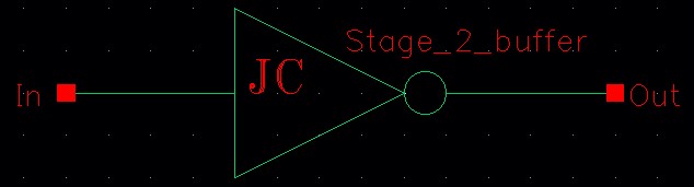 |
| Entire layout |  |
| Close up of 1st half | 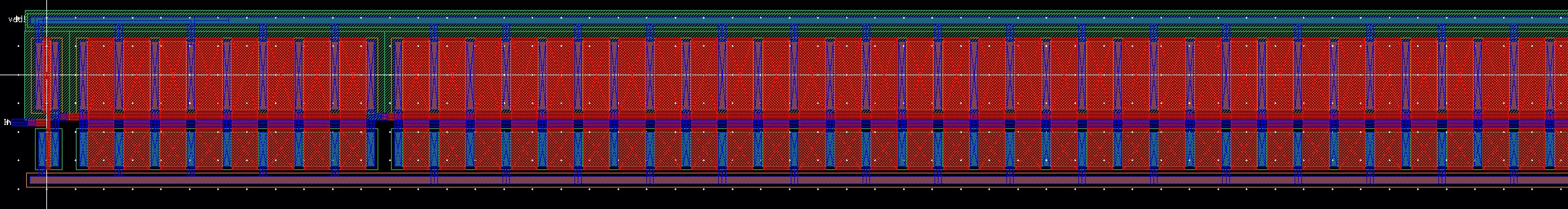 |
| Close up of 2nd half |  |
| DRC | 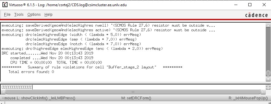 |
| LVS | 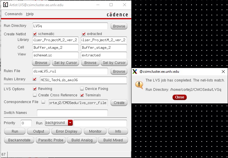 |
Below is the layout for the XOR gate used in the clock multiplier, as well as other relevant screenshots.
| Symbol | 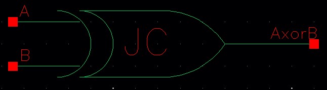 |
| Layout | 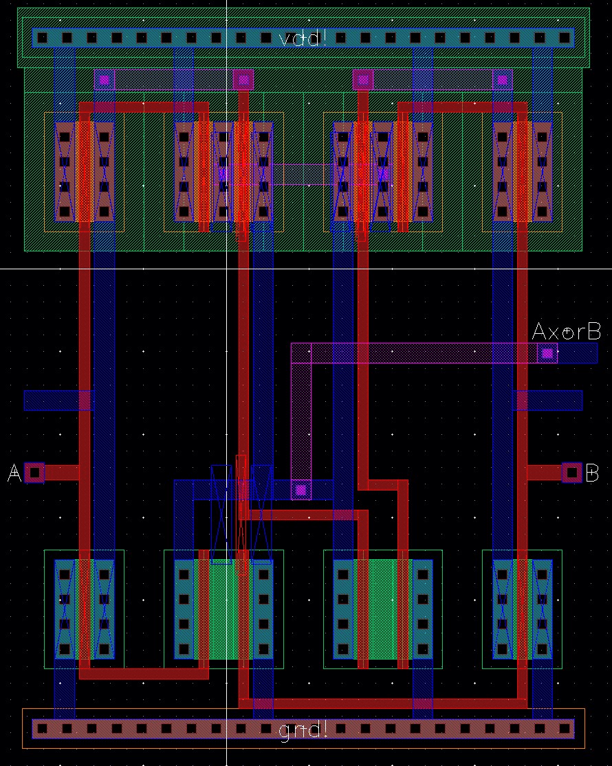 |
| DRC | 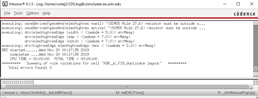 |
| LVS | 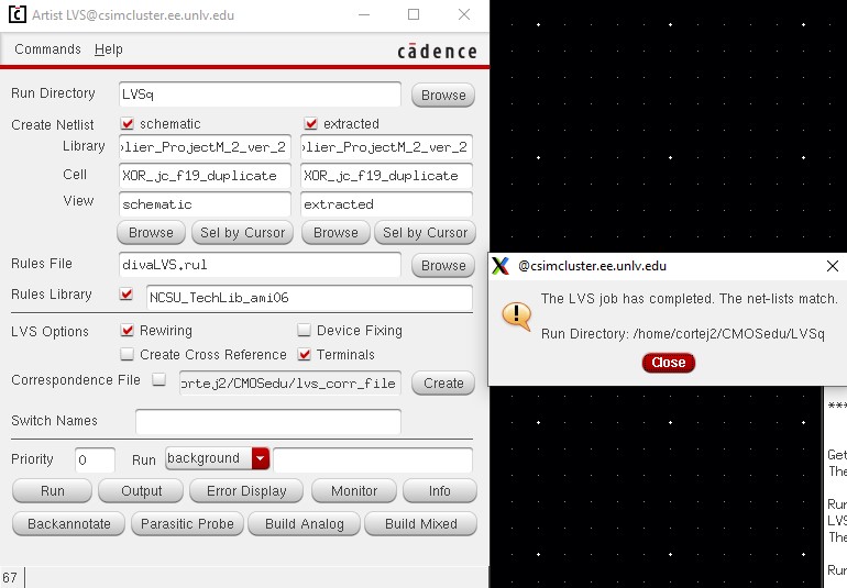 |
Below is the layout for the buffers applied at the right side of the XOR gates, as well as other relevant screenshots.
| Symbol |  |
| Layout | 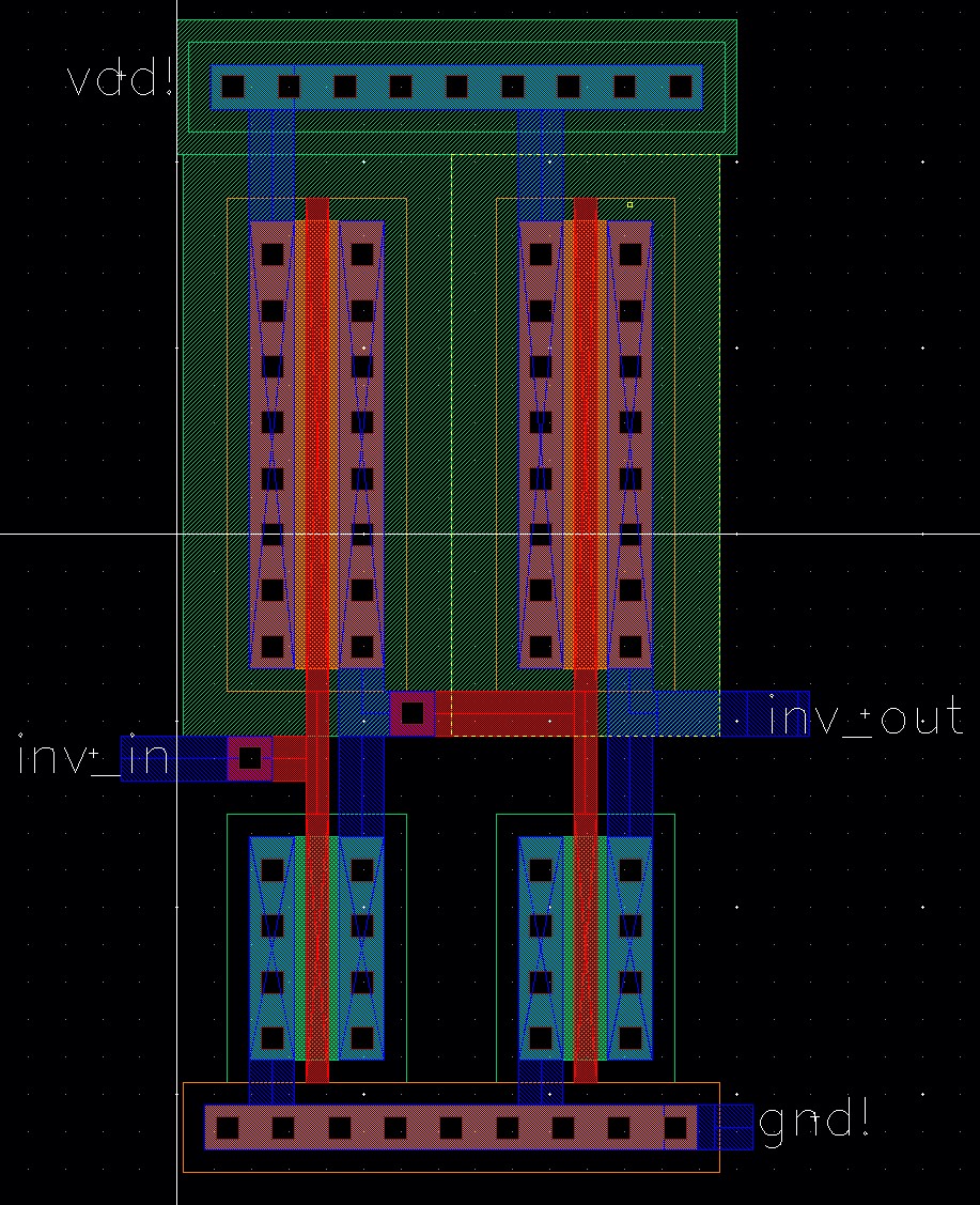 |
| DRC | 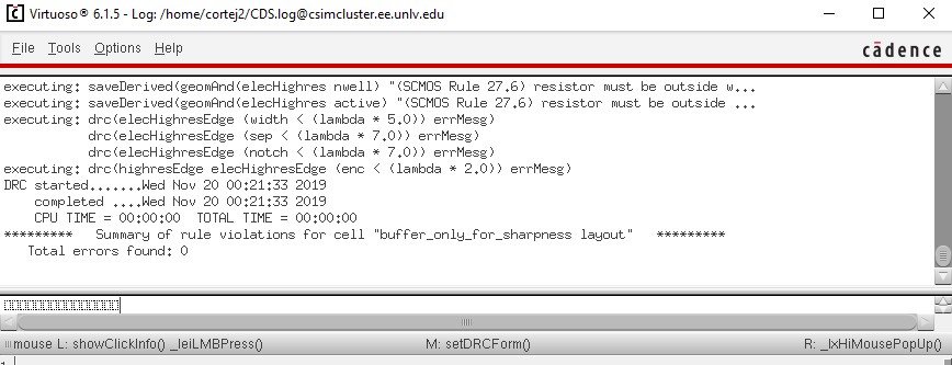 |
| LVS | 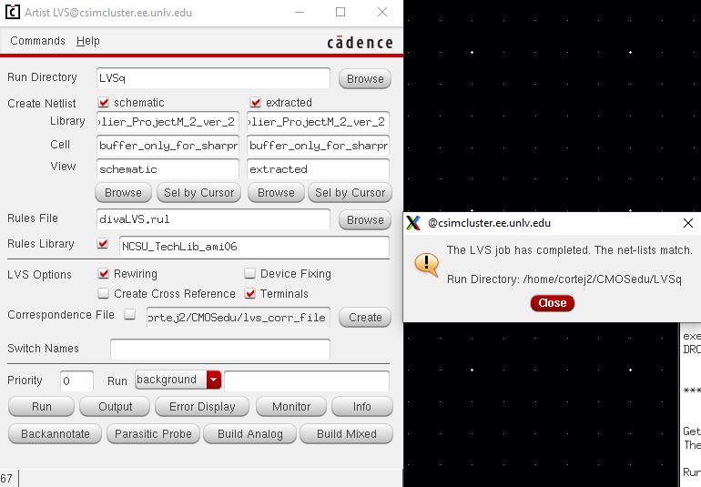 |
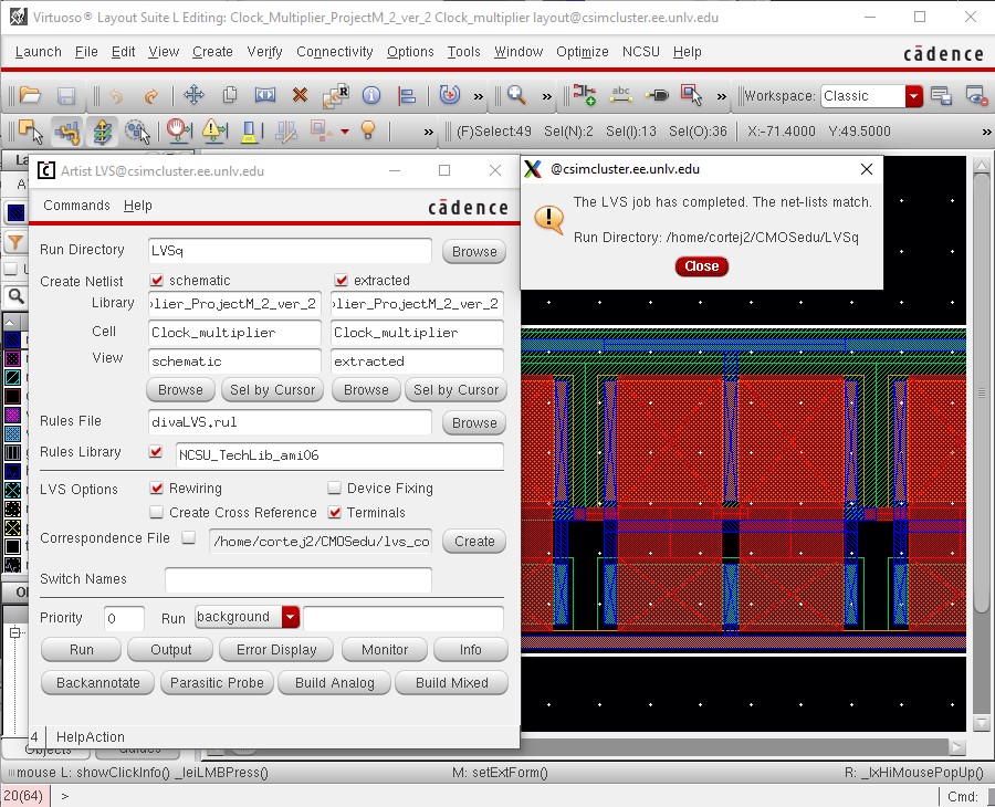
below is the clock multiplier layout

clock mutliplier LVS
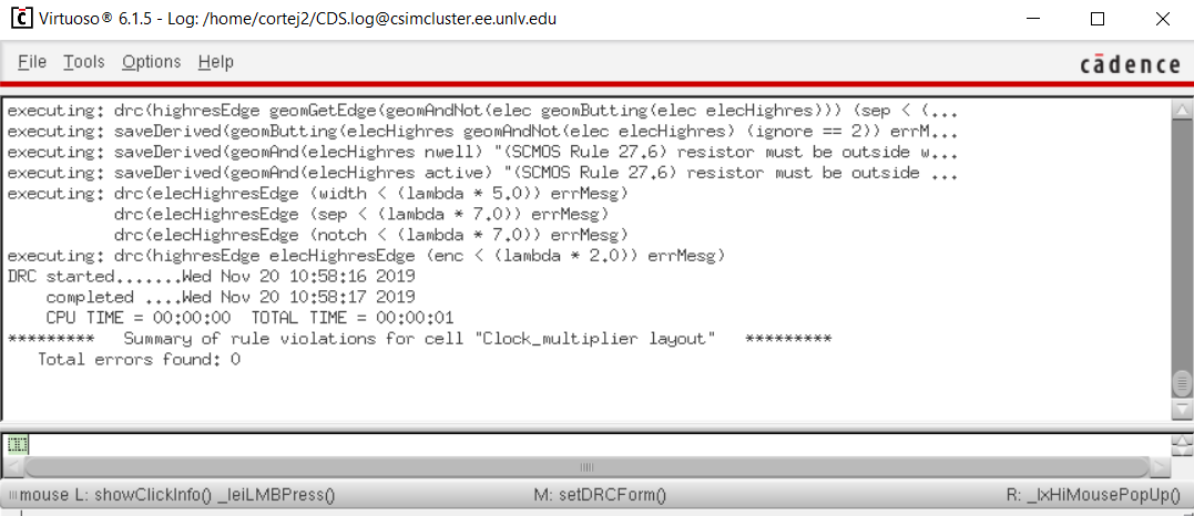
clock multiplier DRC
--------------------------------------------------------------------------------------------------------------------------------------------------------------------------------------------------------------------------------------------------------------
The link to the files can be found here