Lab 7 - ECE 421L
Email Address: cortej2@unlv.nevada.edu
Lab Date: Oct 23,2019-Nov 6,2019
--------------------------------------------------------------------------------------------------------------------------------------------
Prelab:
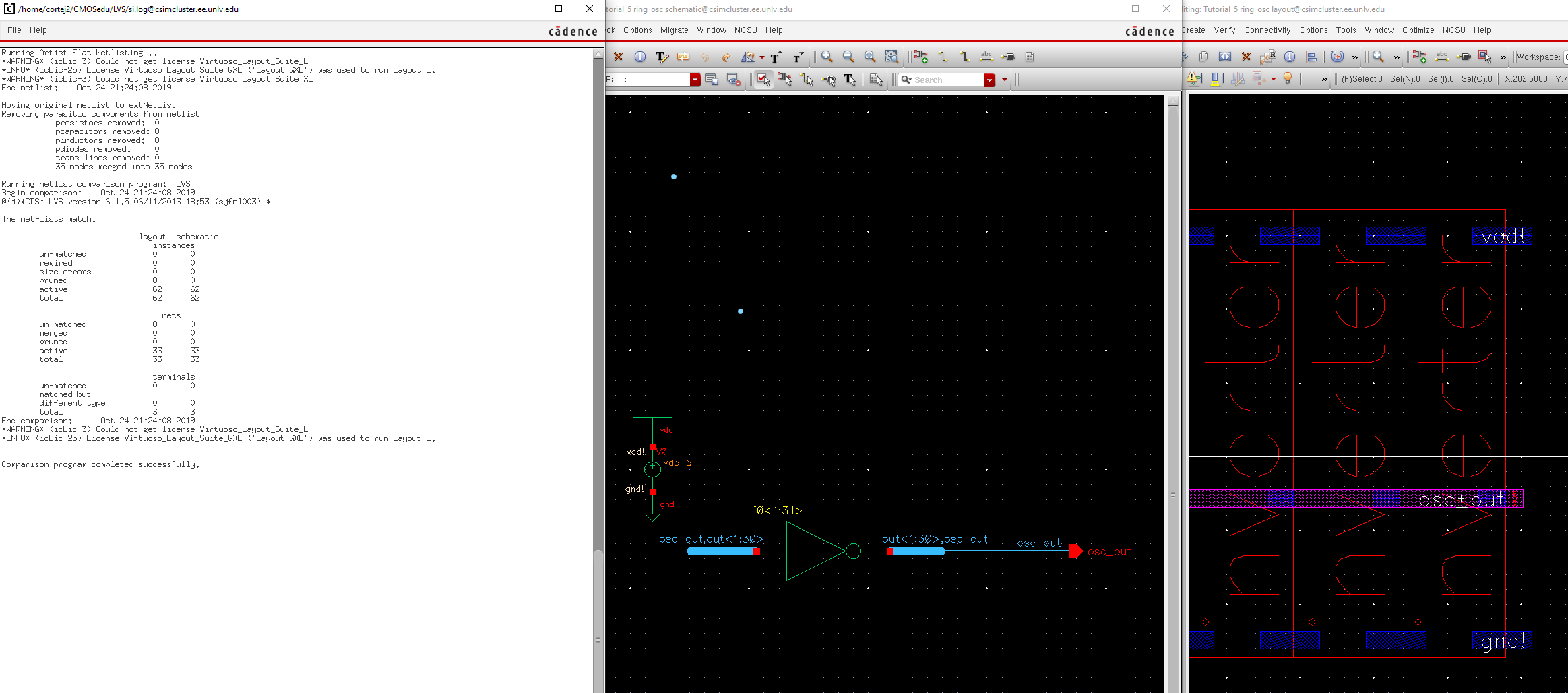
For the prelab, I created the schematic, symbol, layout and extraction of a ring oscillator.
I also simulated the ring oscillator to ensure its functionality.
| Ring Oscillator LVS, Schematic and Layout |
|
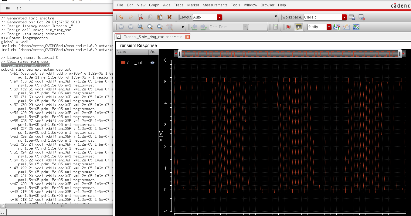
| Ring Oscillator Simulation Results |
 |
--------------------------------------------------------------------------------------------------------------------------------------------
--------------------------------------------------------------------------------------------------------------------------------------------
Lab:
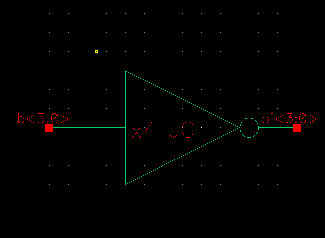
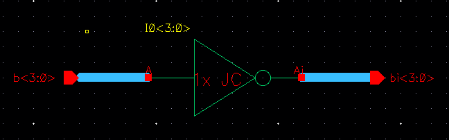
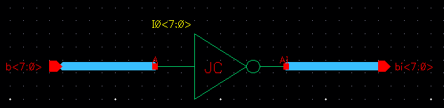
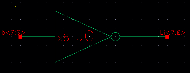
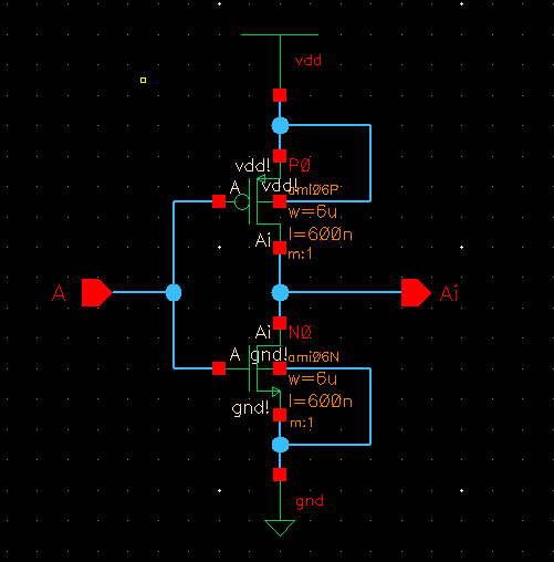
Concise <3:0> inverter
I created a concise 4 bit word inverter, this requires using a wide wire (bus) to connect inputs and outputs.
Below is the symbol,schematic and PMOS and NMOS used.
| 4bit Word Inverter Symbol |
 |
| 4bit Word Inverter Schematic |
 |
| 4bit Word Inverter |
 |
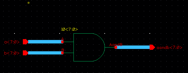
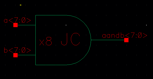
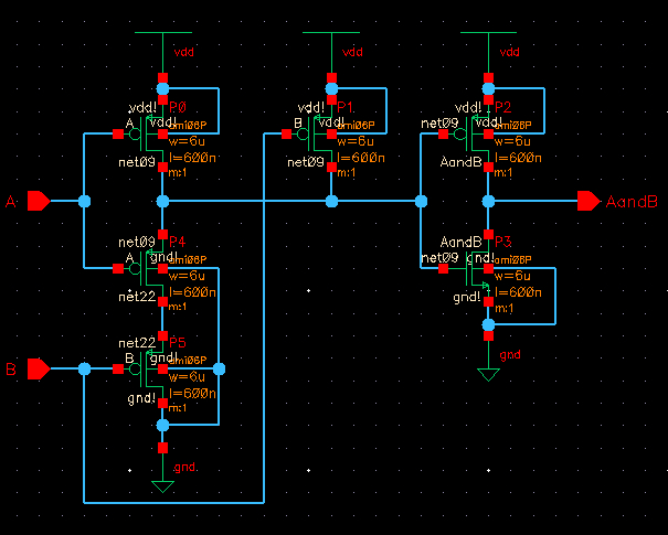
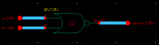
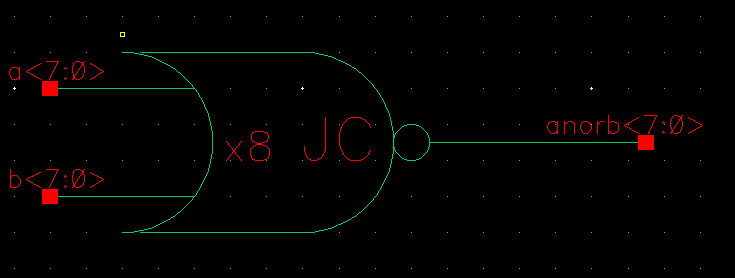
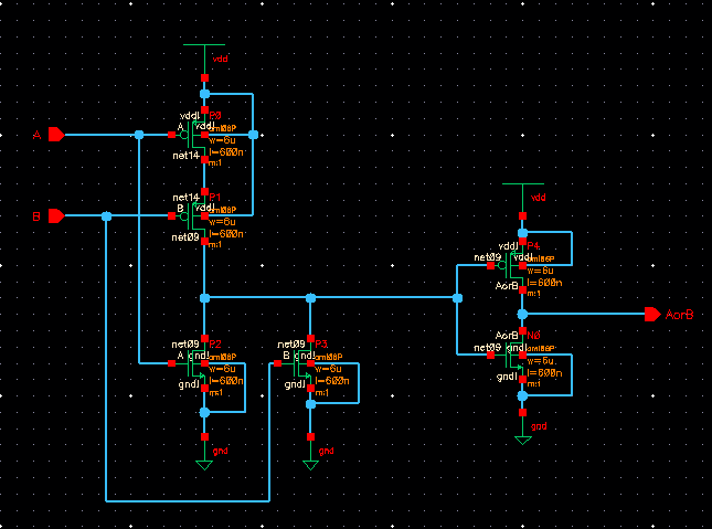
I then created 8-bit arrays made up of NAND, AND, NOR, OR gates as well as inverters.
| 8bit NAND schematic |
 |
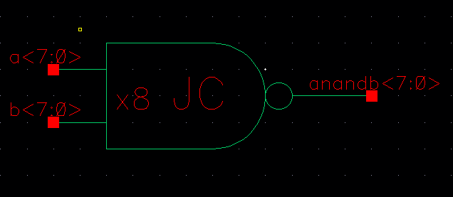
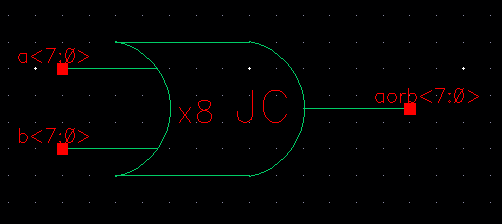
| 8bit NAND symbol |
 |
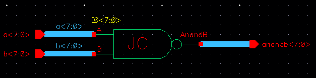
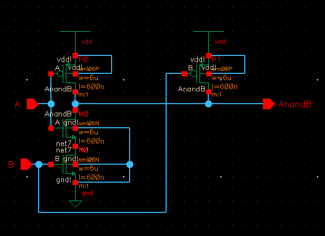
| Single NAND schematic |
 |
| 8bit AND schematic |
 |
| 8bit AND symbol |
 |
| Single AND schematic |
 |
| 8bit NOR schematic |
 |
| 8bit NOR symbol |
 |
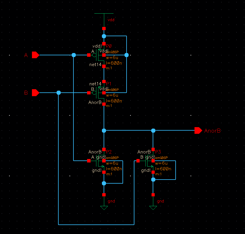
| single NOR schematic |
 |
| 8bit OR schematic |
 |
| 8bit OR symbol |
 |
| single OR schematic |
 |
| 8bit inverter schematic |
 |
| 8bit inverter symbol |
 |
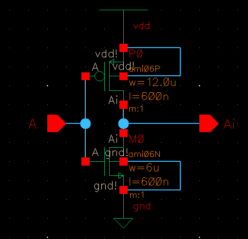
| single inverter schematic |
 -------------------------------------------------------------------------------------------------------------------------------------------- |
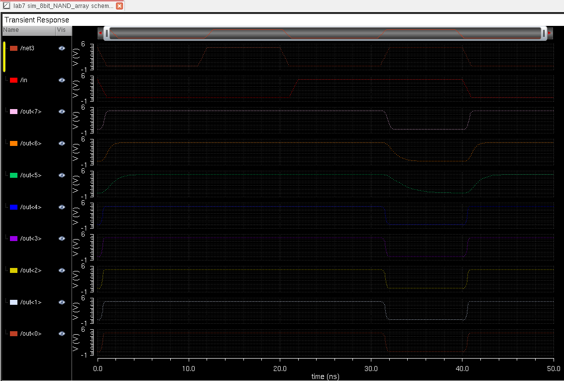
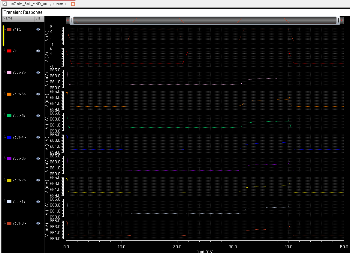
I then simulated each of the gates and inverter to see how the output would behave if I were to input 00,01,10,11 into the gates and inverter.
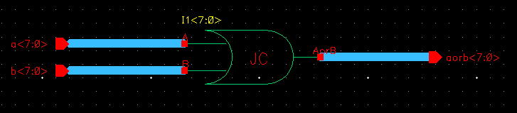
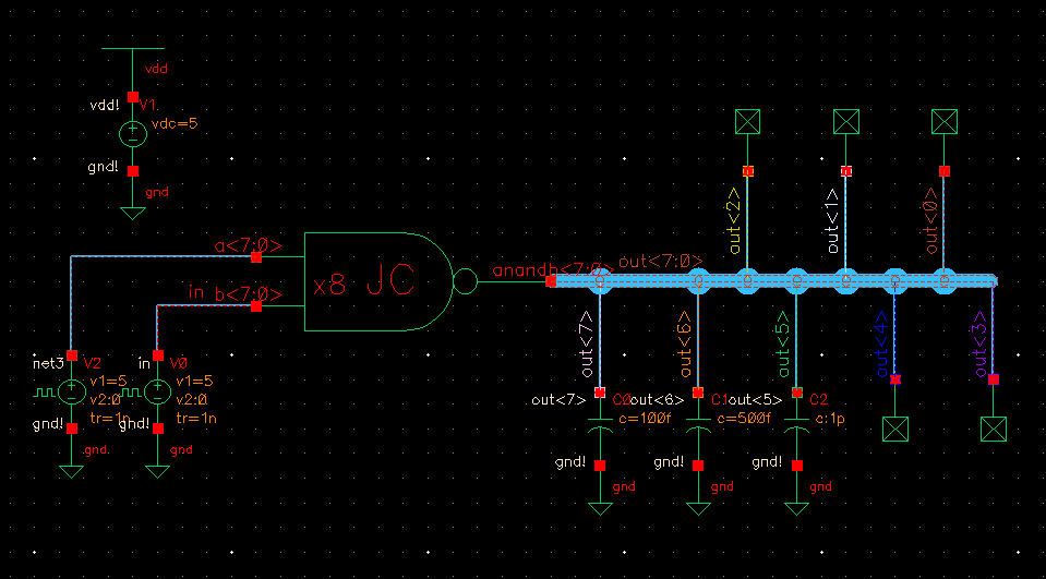
| 8bit NAND simulation schematic |
 |
| 8bit NAND simulation results |
 |
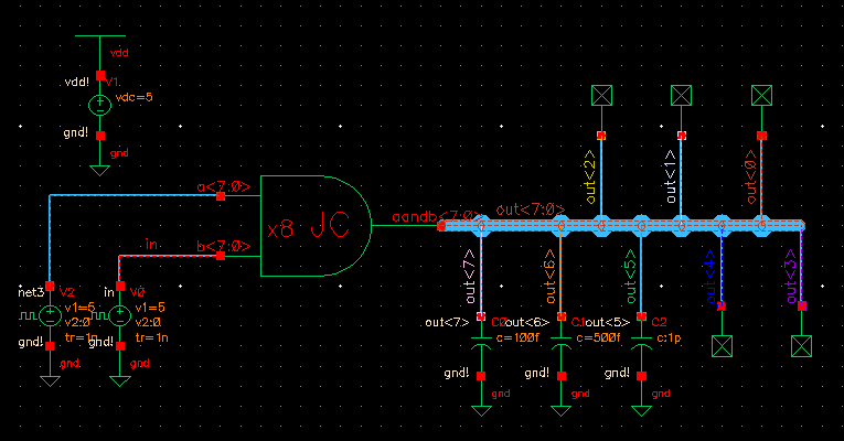
| 8bit AND simulation schematic |
 |
| 8bit AND simulation results |
 |
| 8bit NOR simulation schematic |
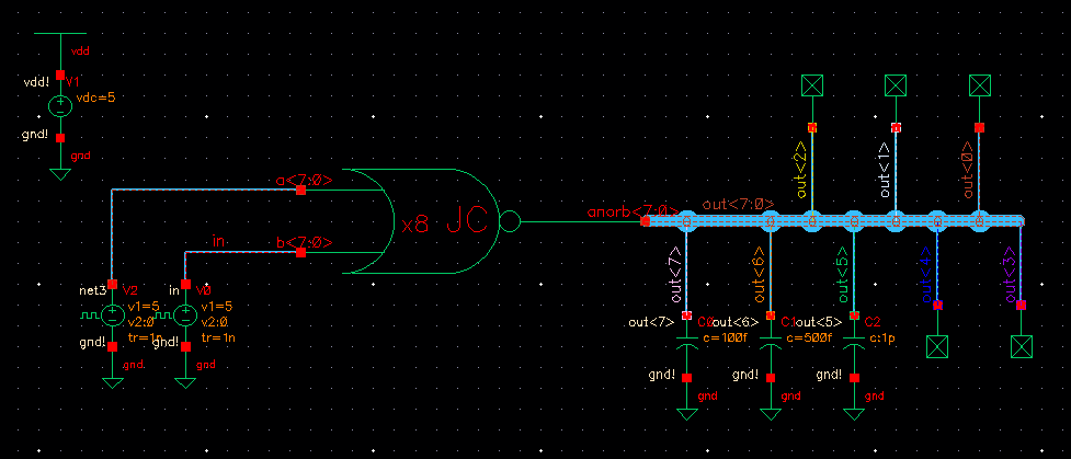 |
| 8bit NOR simulation results |
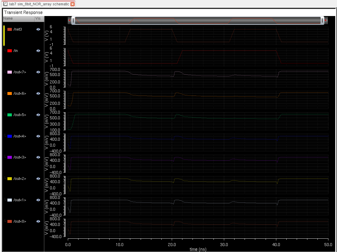 |
| 8bit OR simulation schematic |
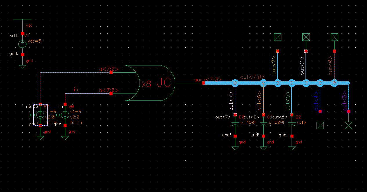 |
| 8bit OR simulation results |
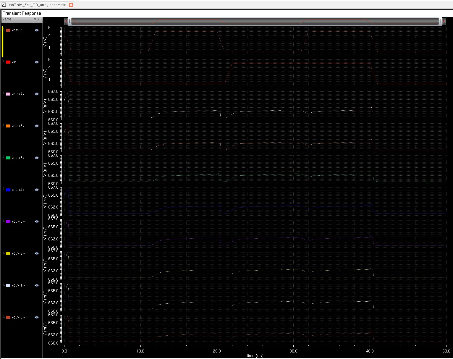 |
--------------------------------------------------------------------------------------------------------------------------------------------
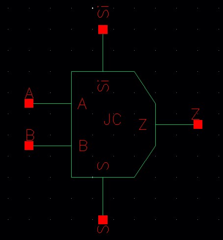
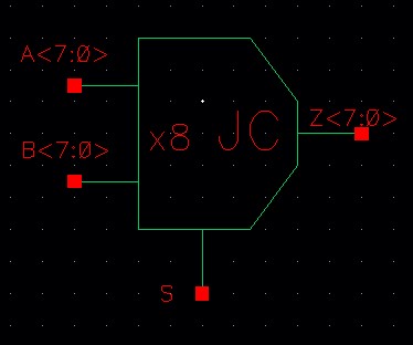
| DEMUX/MUX symbol |
 |
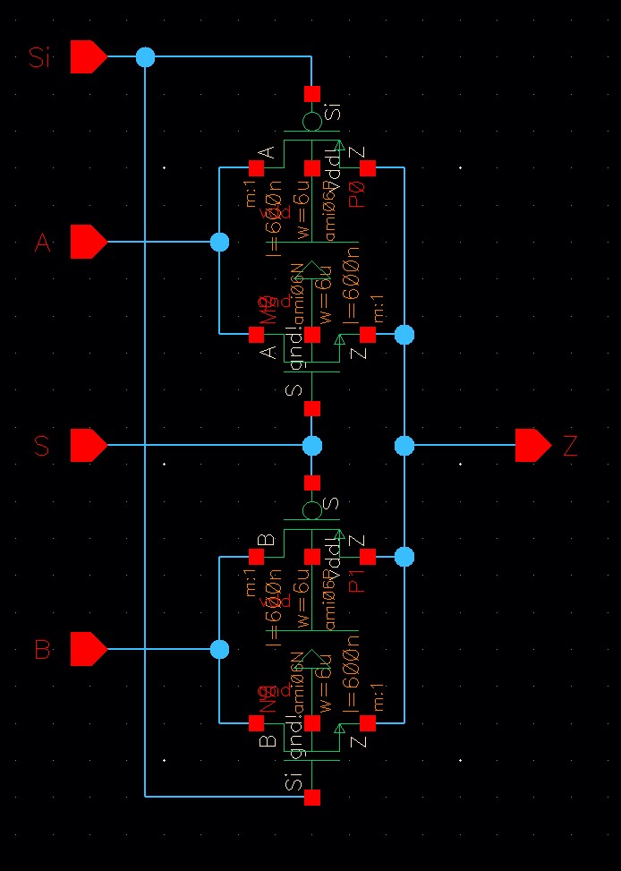
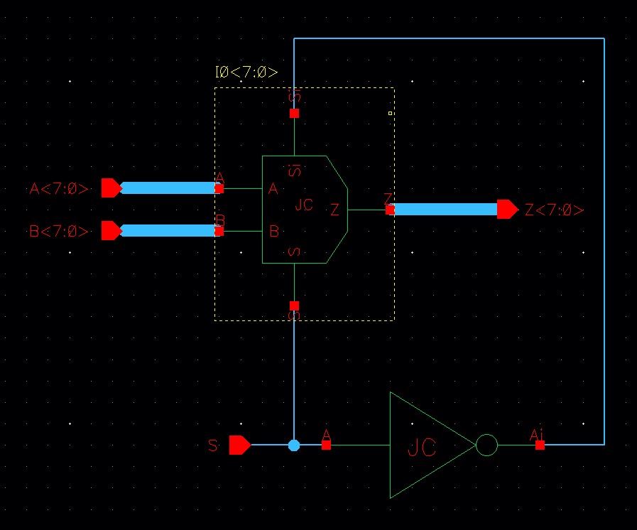
| DEMUX/MUX schematic |
 |
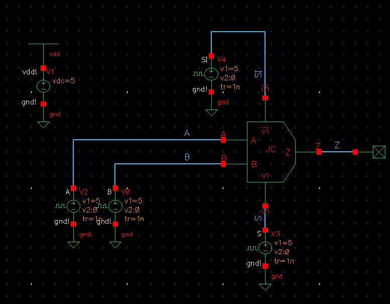
I then simulated the DEMUX/MUX to understand how it behaves with certain input.
| DEMUX/MUX simulation schematic |
 |
| DEMUX/MUX simulation results |
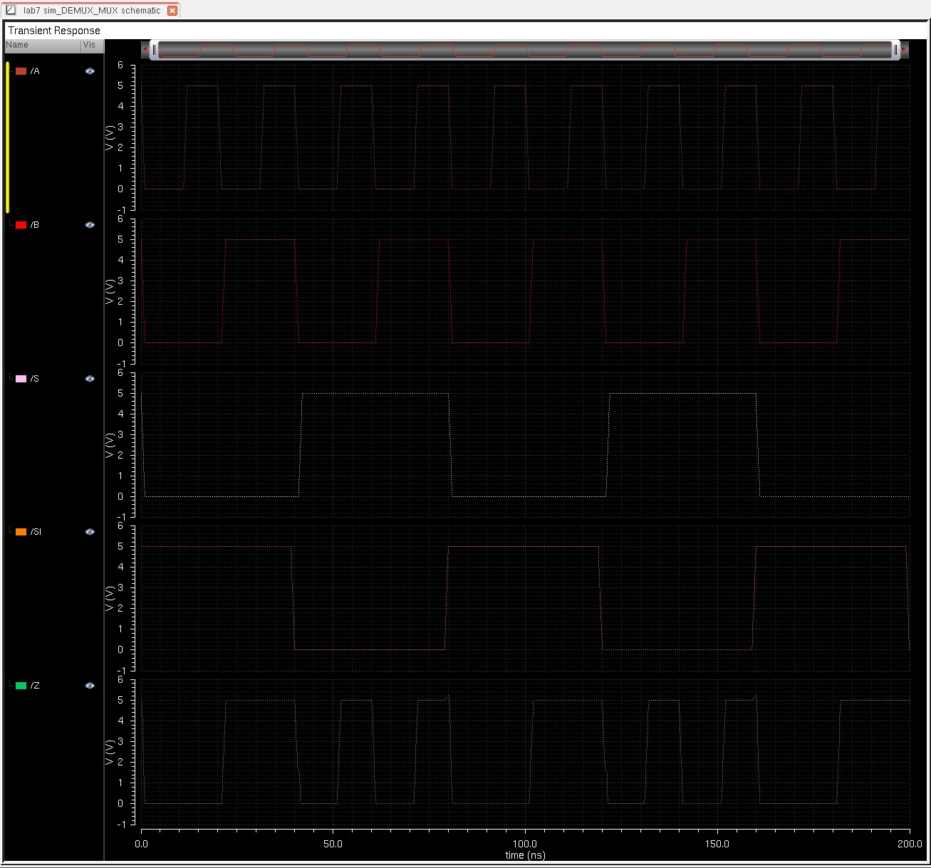 |
we can observe from the output simulation of the MUX that as the input Select is '1', 'A' becomes the active input and passes the output value.
In the same context, when the Select is set to '0', 'B' becomes the active input and passes the output value of the MUX.
Therefore, the logical operation 'Z = A*S + B*Si' is a suffice logical operation.
For a DEMUX operation, instead, the output is chosen to select the input line 'A' or 'B'.
--------------------------------------------------------------------------------------------------------------------------------------------
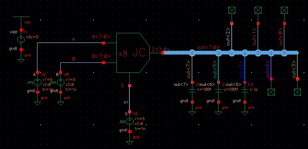
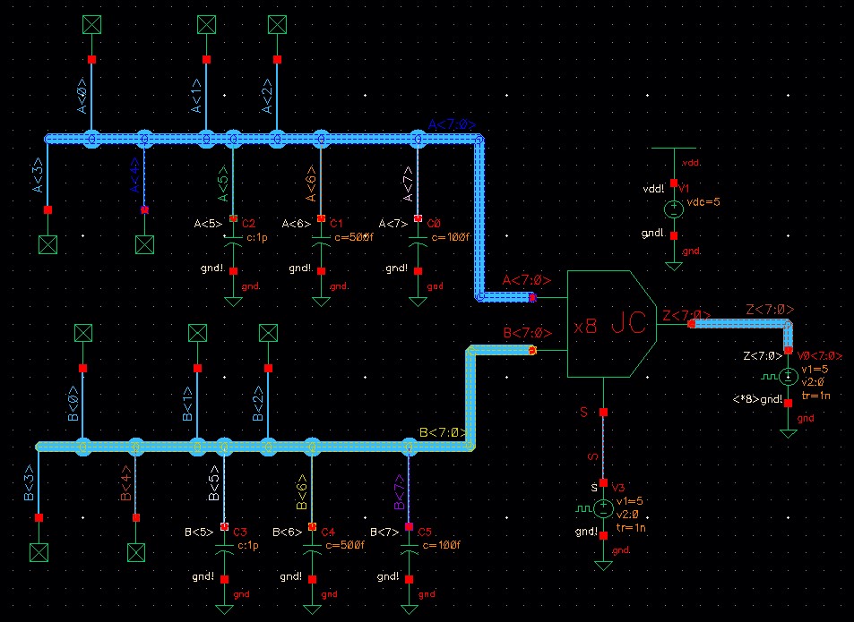
I then created an 8bit_DEMUX/MUX schematic and symbol as shown below.
| 8bit DEMUX/MUX schematic |
 |
| 8bit DEMUX/MUX symbol |
 |
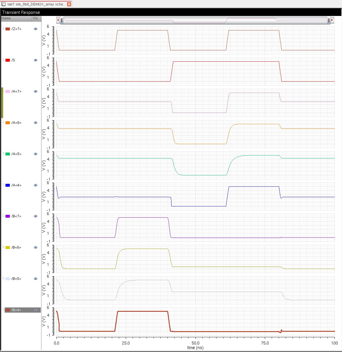
I then created a schematic to demonstrate its capabilities as a MUX.
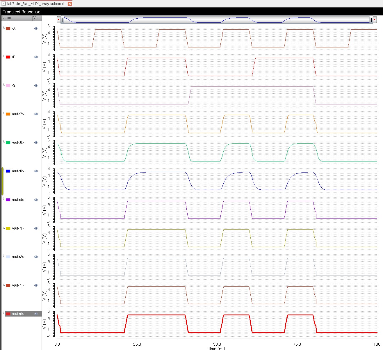
| MUX simulation schematic |
 |
| MUX simulation results |
 |
I then created a schematic to demonstrate its capabilities as a DEMUX.
| DEMUX simulation schematic |
 |
| DEMUX simulation results |
 |
--------------------------------------------------------------------------------------------------------------------------------------------
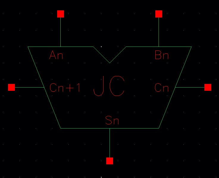
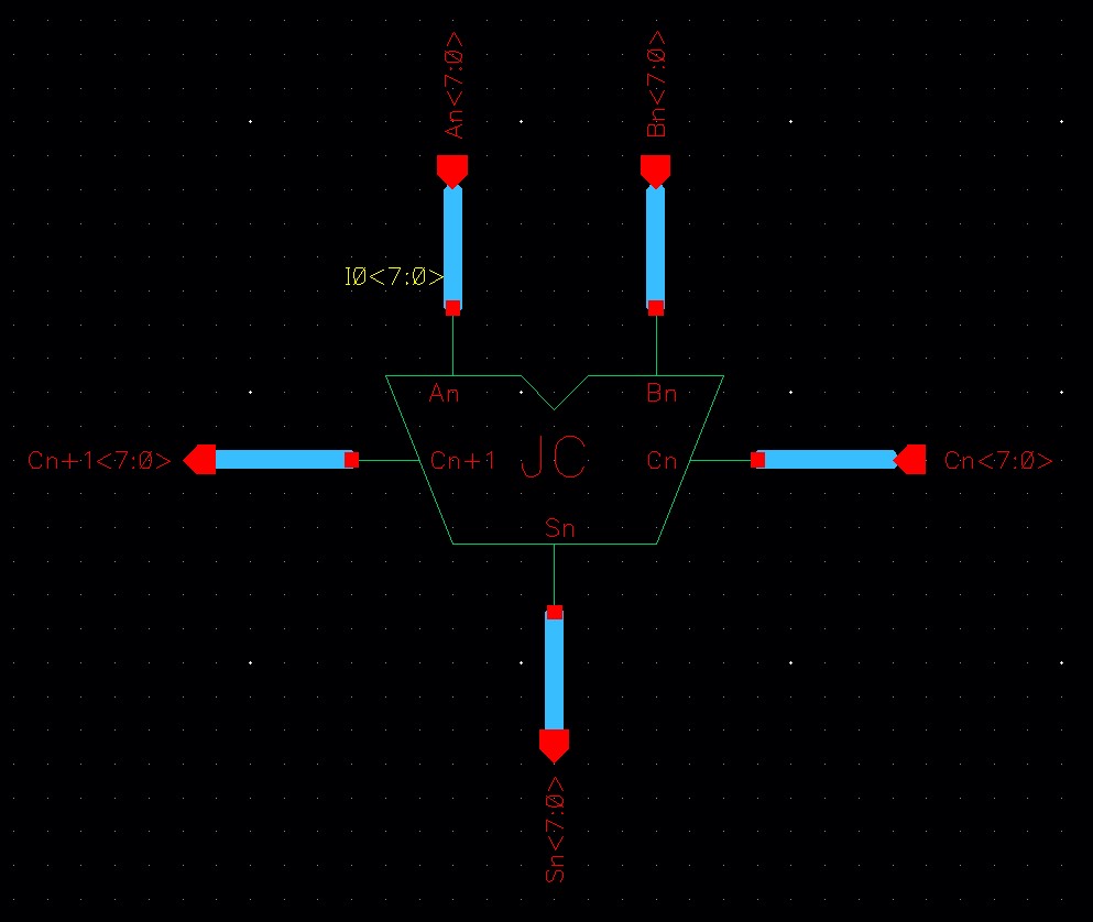
I then created the schematic and symbol for the full adder found in figure 12.20 using 6u/0.6u devices.
| full adder schematic |
 |
| full adder symbol |
 |
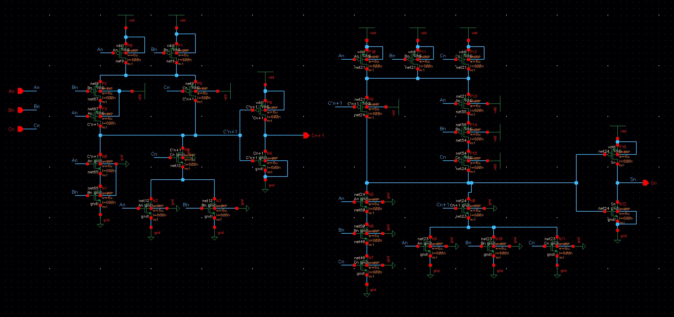
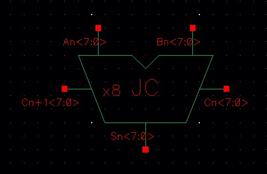
I then created an 8bit version of the full adder with layout
| 8bit full adder schematic |
 |
| 8bit full adder symbol |
 |
| 8bit full adder layout |
 |
--------------------------------------------------------------------------------------------------------------------------------------------