Lab 4 - ECE 421L
-------------------------------------------------------------------------------------------------------------------------------------
Prelab:
For the prelab I went through tutorial 2 which involved creating
schematics, symbols and layouts for NMOS and PMOS transistors
and analyzing them.
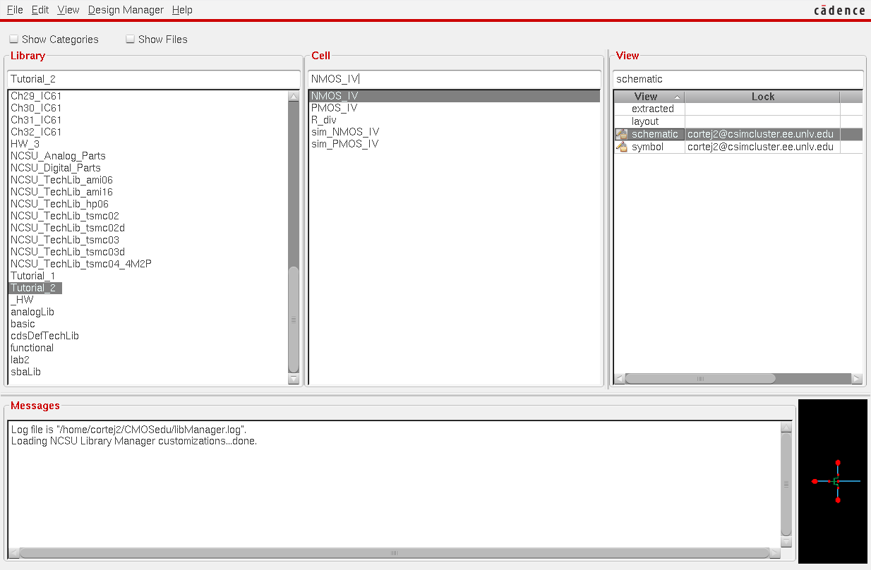
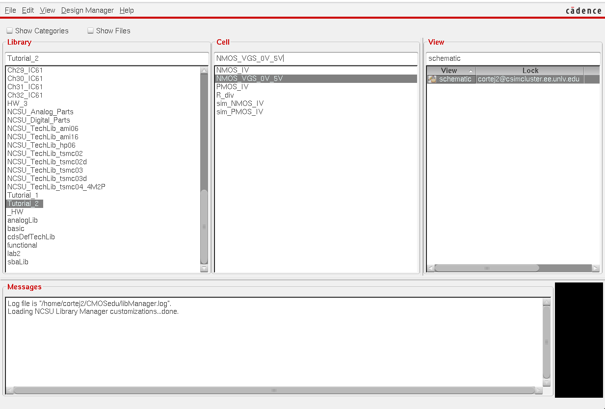
I began by creating creating a new folder where the tutorial files will
be placed, the file is a copy of tutorial 1 and are shown below.
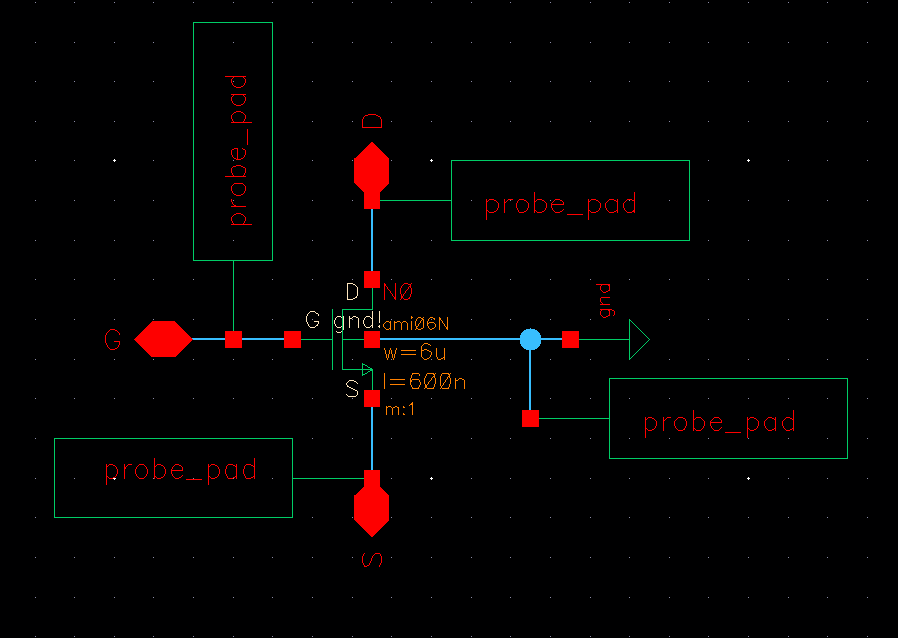
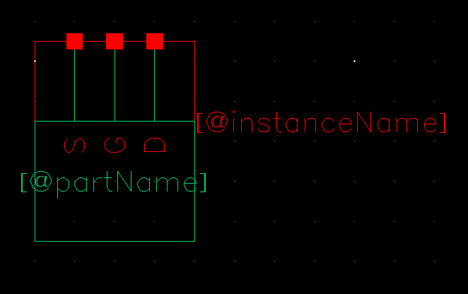
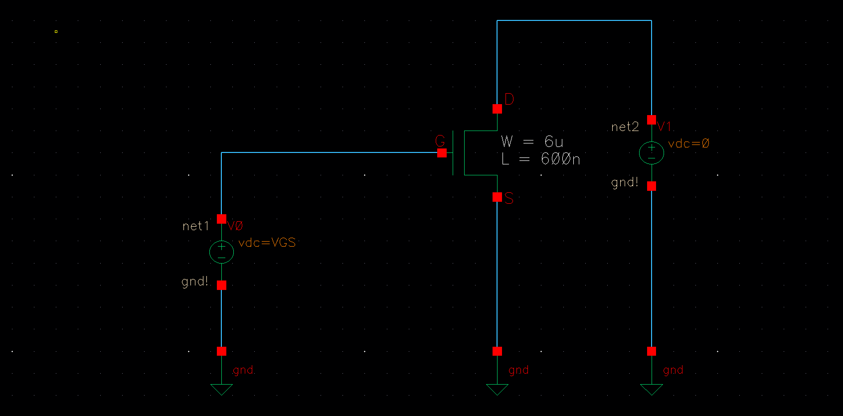
I then created a schematic and symbol for an NMOS transistor, the symbol is shown below
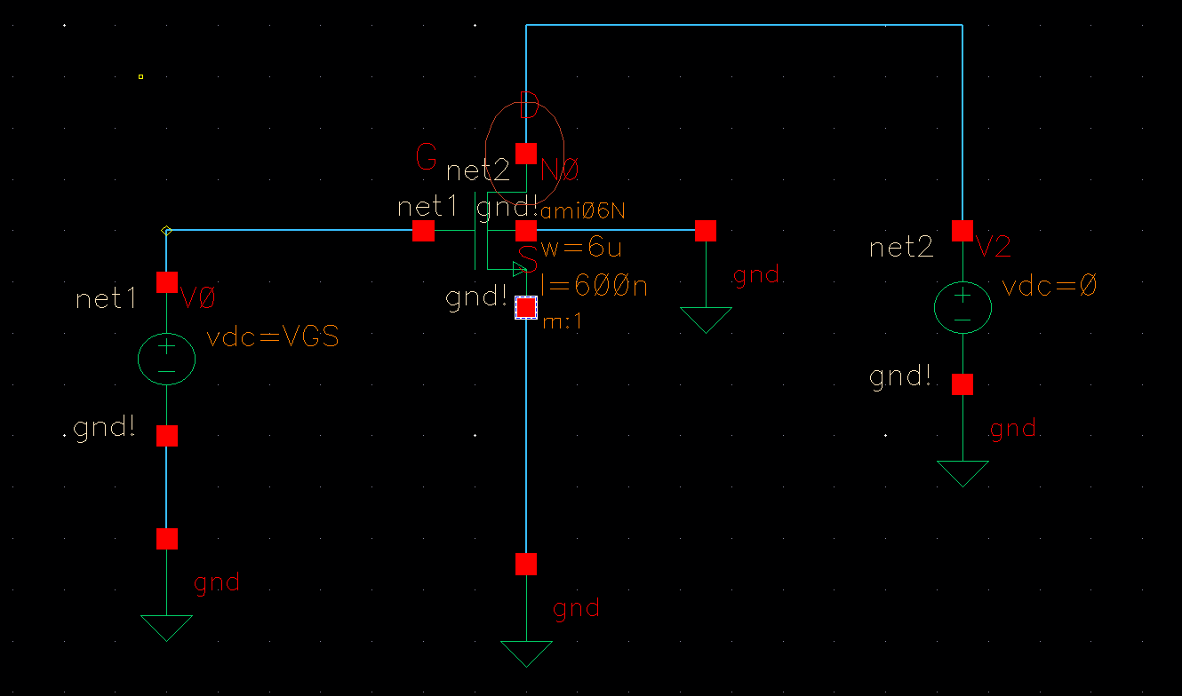
After that I made a schematic to simulate the NMOS symbol. Below is the schematic.
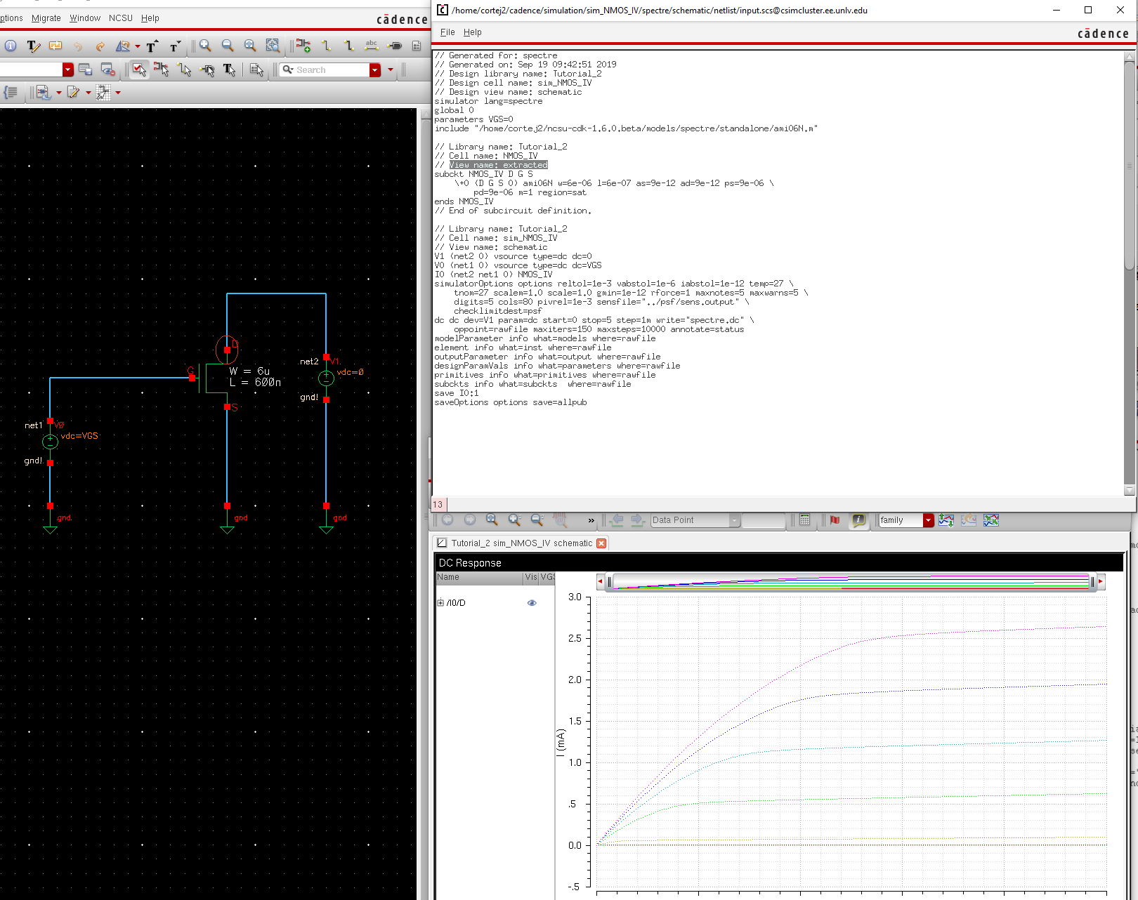
I ran a simulation of the extracted view, after the simulation and looked
at the netlist through tools-->netlist-->display to ensure the
extracted view was simulated.
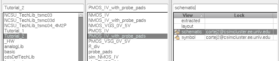
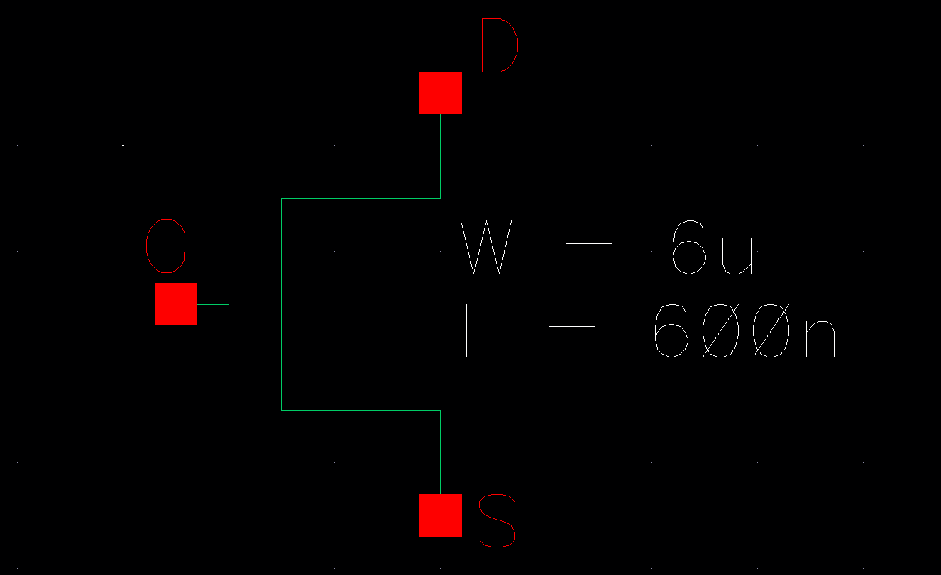
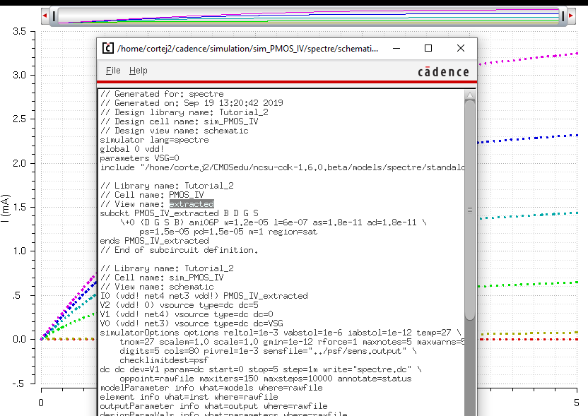
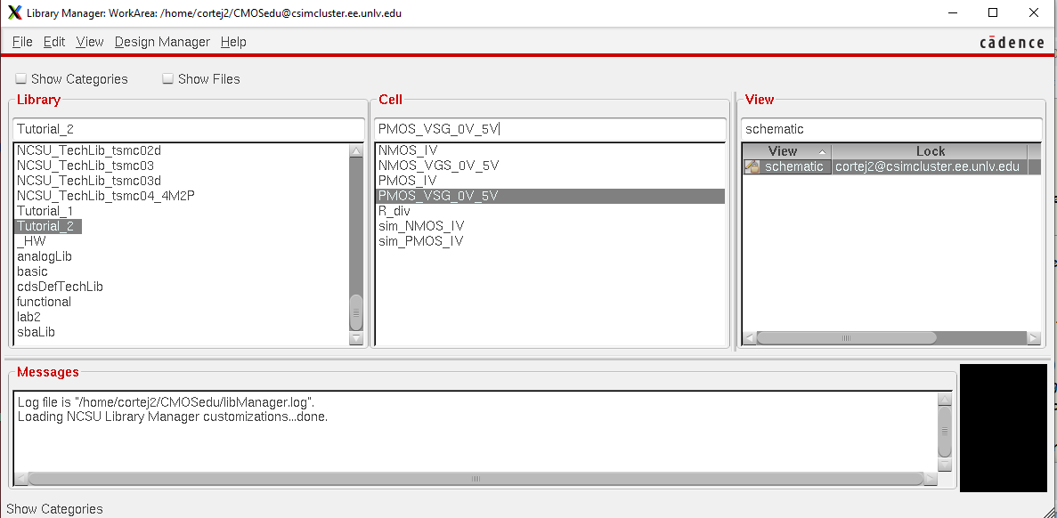
I then created a schematic cell view called PMOS_IV with a width of 12 um and length of 600 nm.
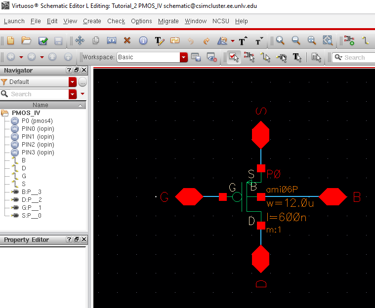
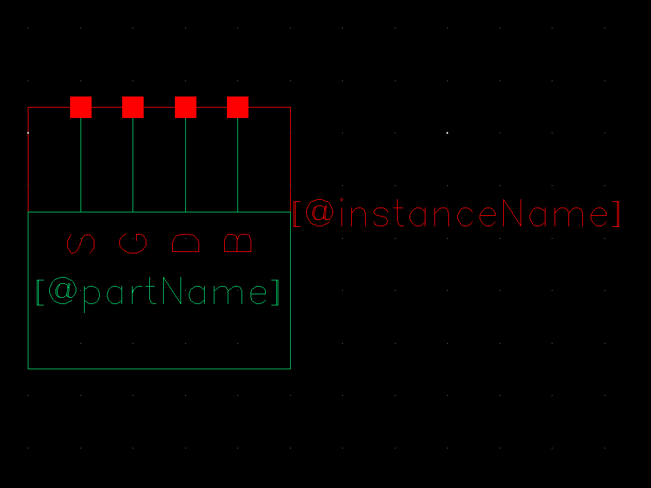
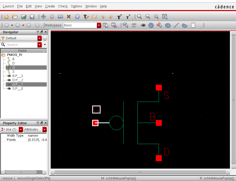
After that I created a symbol for the PMOS, it both have four pins.
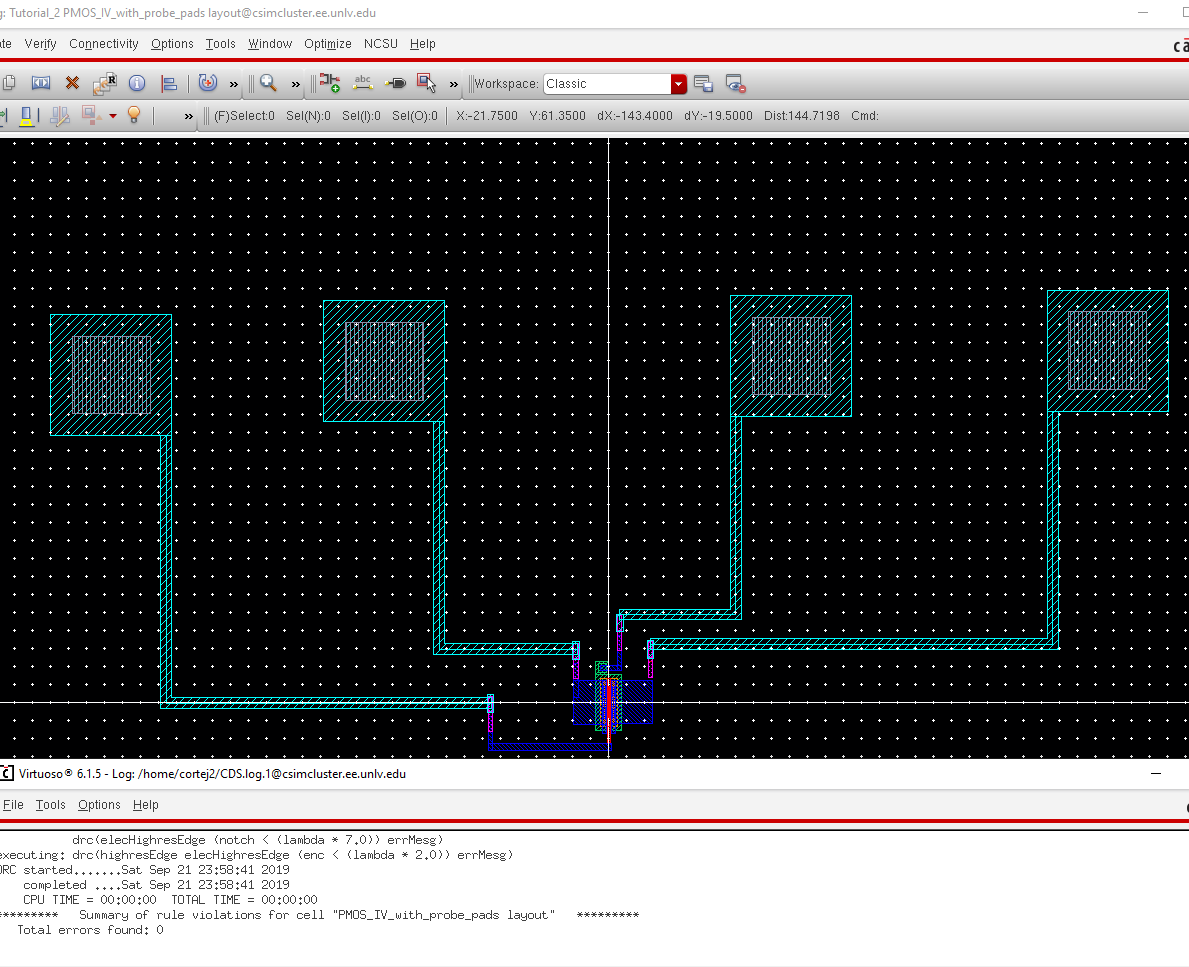
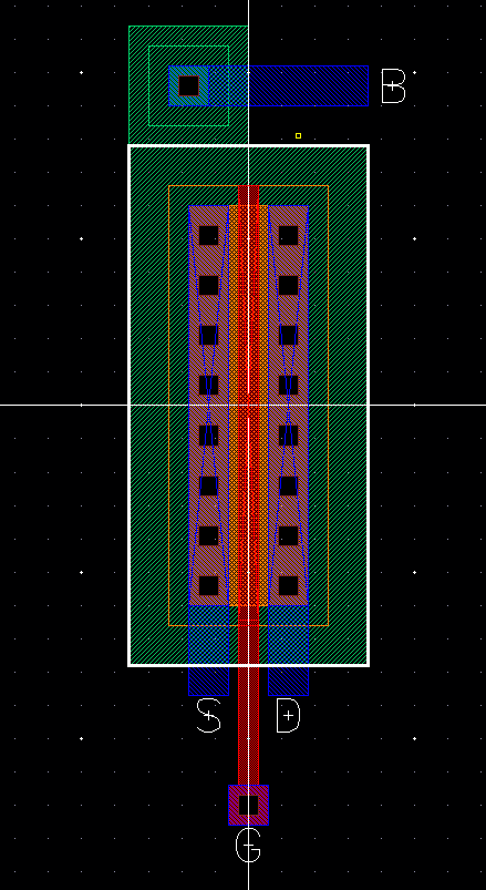
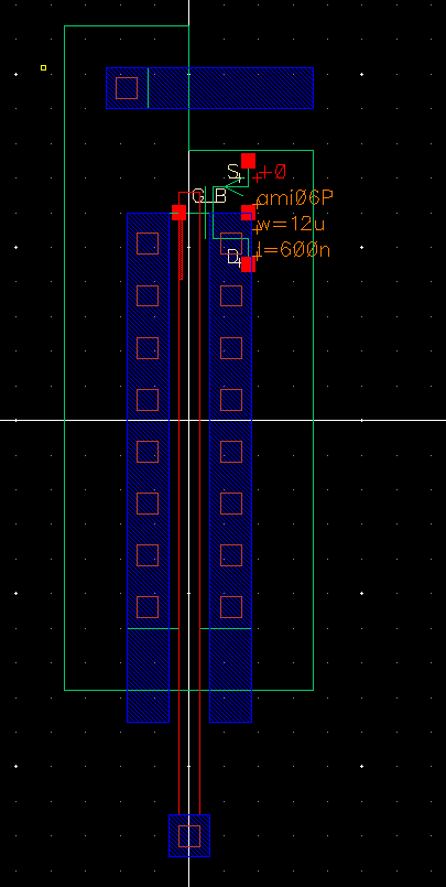
Then I created the layout for the PMOS as shown below
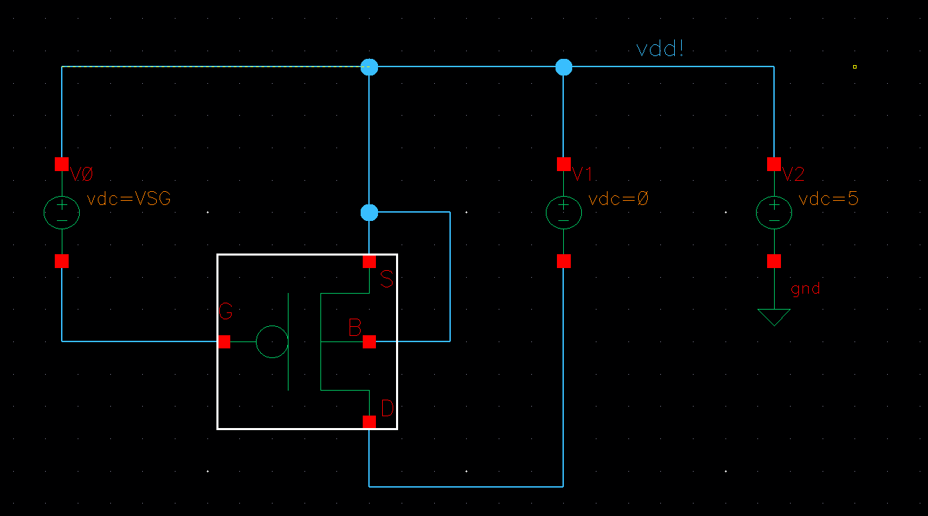
I then attempted to simulate the PMOS I created, I started with a new schematic called sim_PMOS_IV
and recreated the schematic shown in lab 2. Below is the schematic I created.
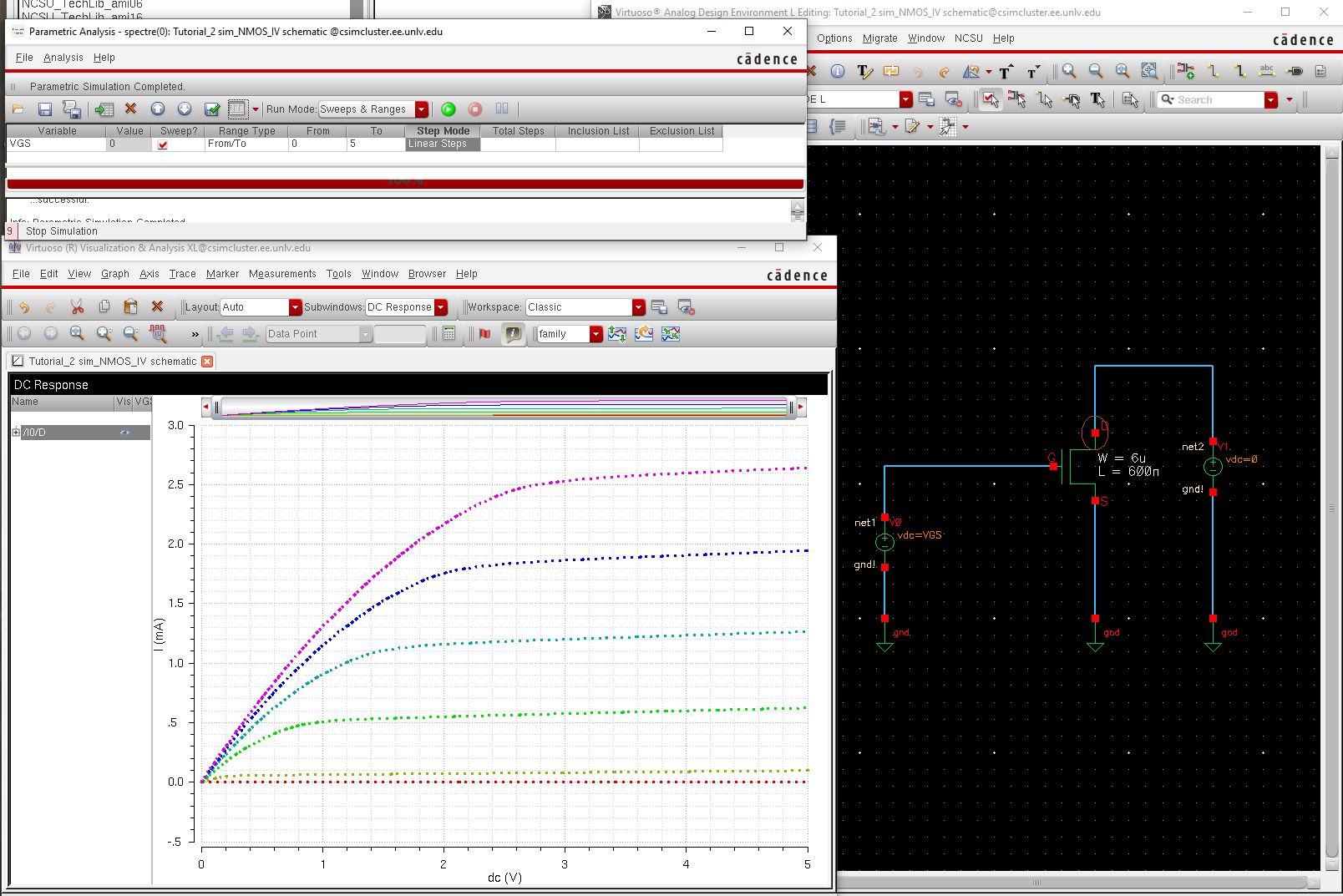
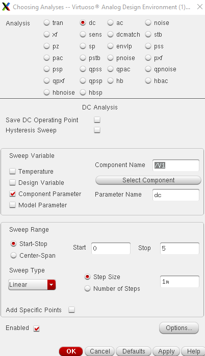
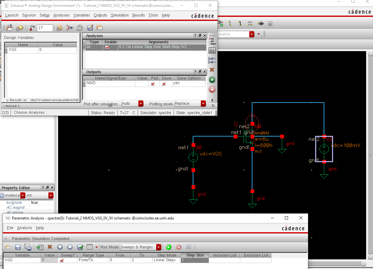
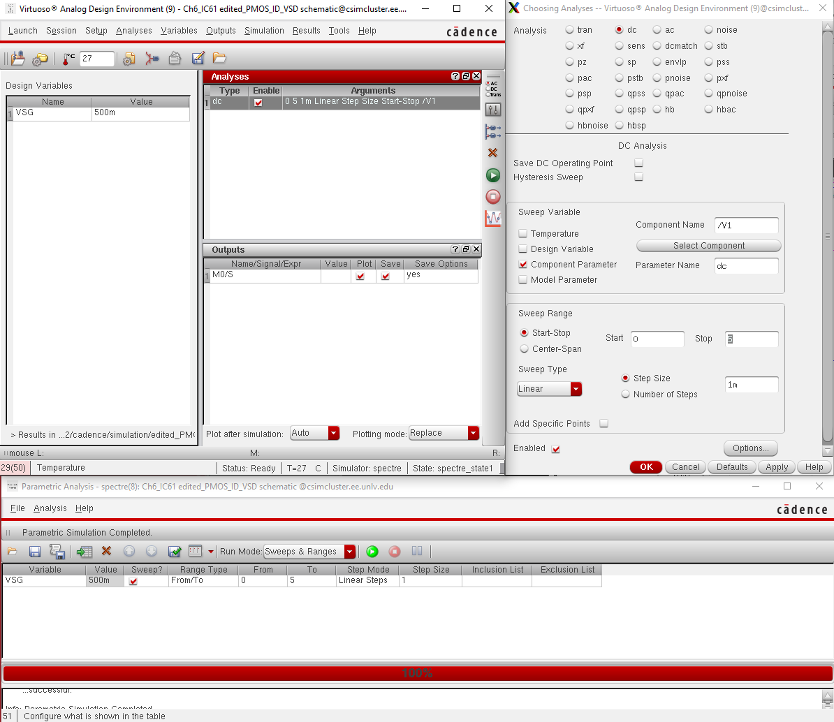
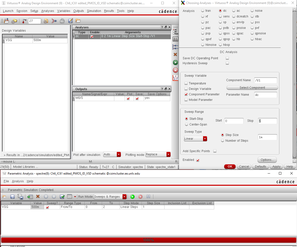
I then ran a parametric analysis on the PMOS circuit, one of the dc
sources is named differently from the tutorial instructions
(in my circuit is is V1 instead of V0 from the instructions) so the dc settings for the analysis are different.
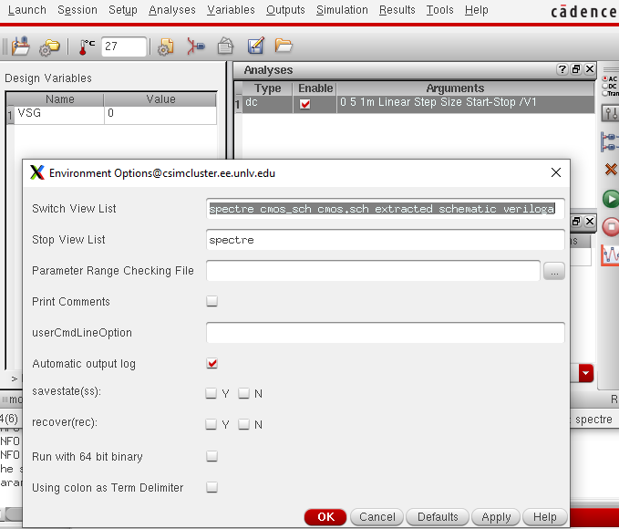
I then went through the analog design environment window to change the environment settings
(through setup--->environment) to change the analysis order. I typed extracted before schematic
in the switch view list so that the extracted view may be analyzed before the schematic.
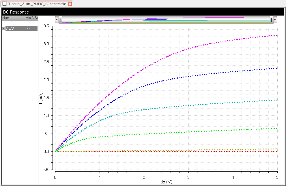
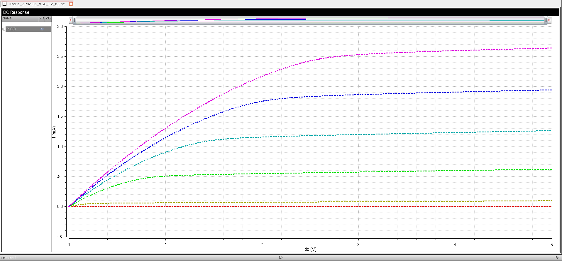
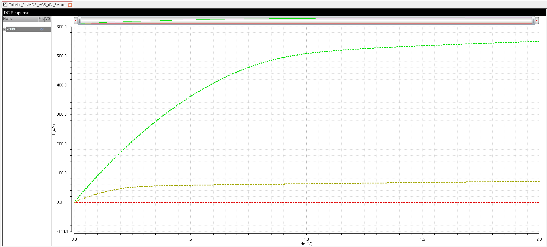
Below are the DC settings, IV curves generated, and environment settings.
-------------------------------------------------------------------------------------------------------------------------------------
Lab: Parts 1) 2) 3)
I started by creating a cellview in the Tutorial 2 folder, this cell view is used to simulate the first two NMOS schematics
First schematic and simulation:
I then created a schematic with an NMOS with width and length of
6um/600nm with VGS varying from 0 to 5 V in 1 V steps while VDS varying
from 0 to 5 V in 1 mV steps.
The settings for the parametric analysis are very similar to the ones in
the prelab, the process for creating the simulation was the same.
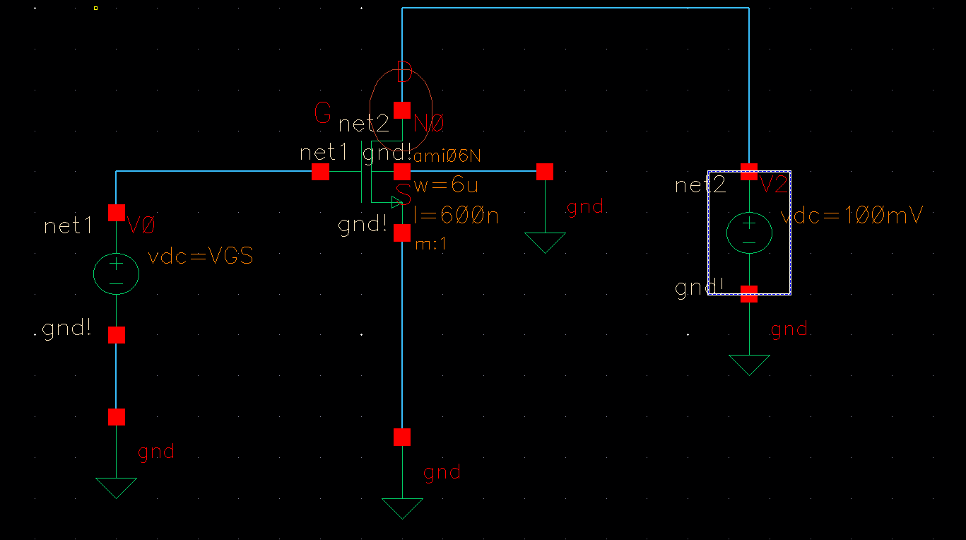
Second schematic and simulation:
I then simulated the same schematic, with some adjustments. I simulated
for when VDS=100 mV and VGS varies from 0 to 2 V in 1 mV steps.
Third schematic and simulations:
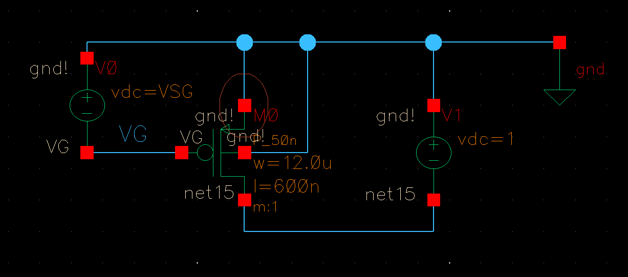
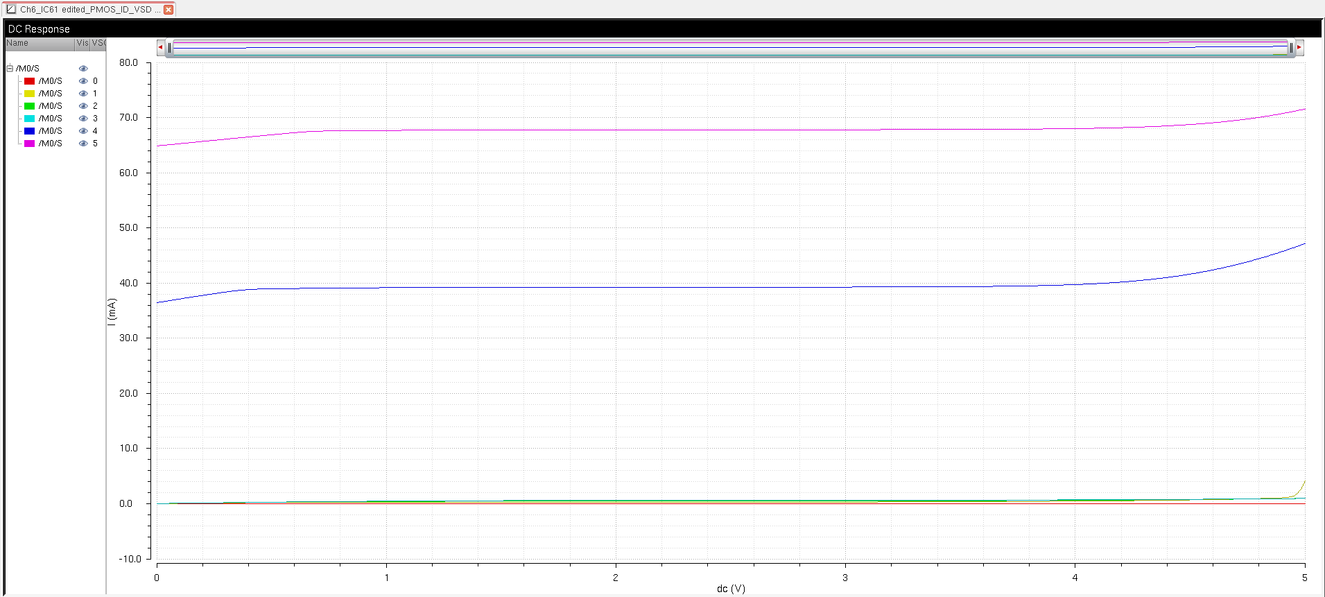
I then created a PMOS schematic that would simulate the ID v VSD curves
for when VSG varies from 0 to 5V in 1V steps while VSD varies from
0 to 5V in 1mV steps. The PMOS used is 12u/600n in width and length.
Fourth schematic and simulations:
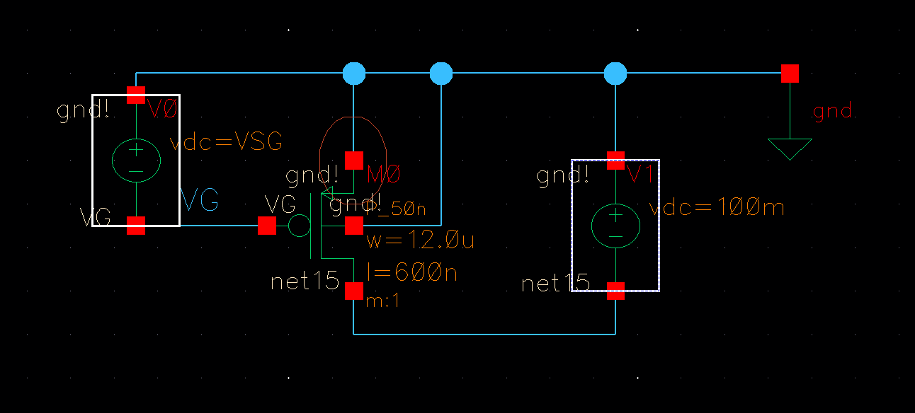
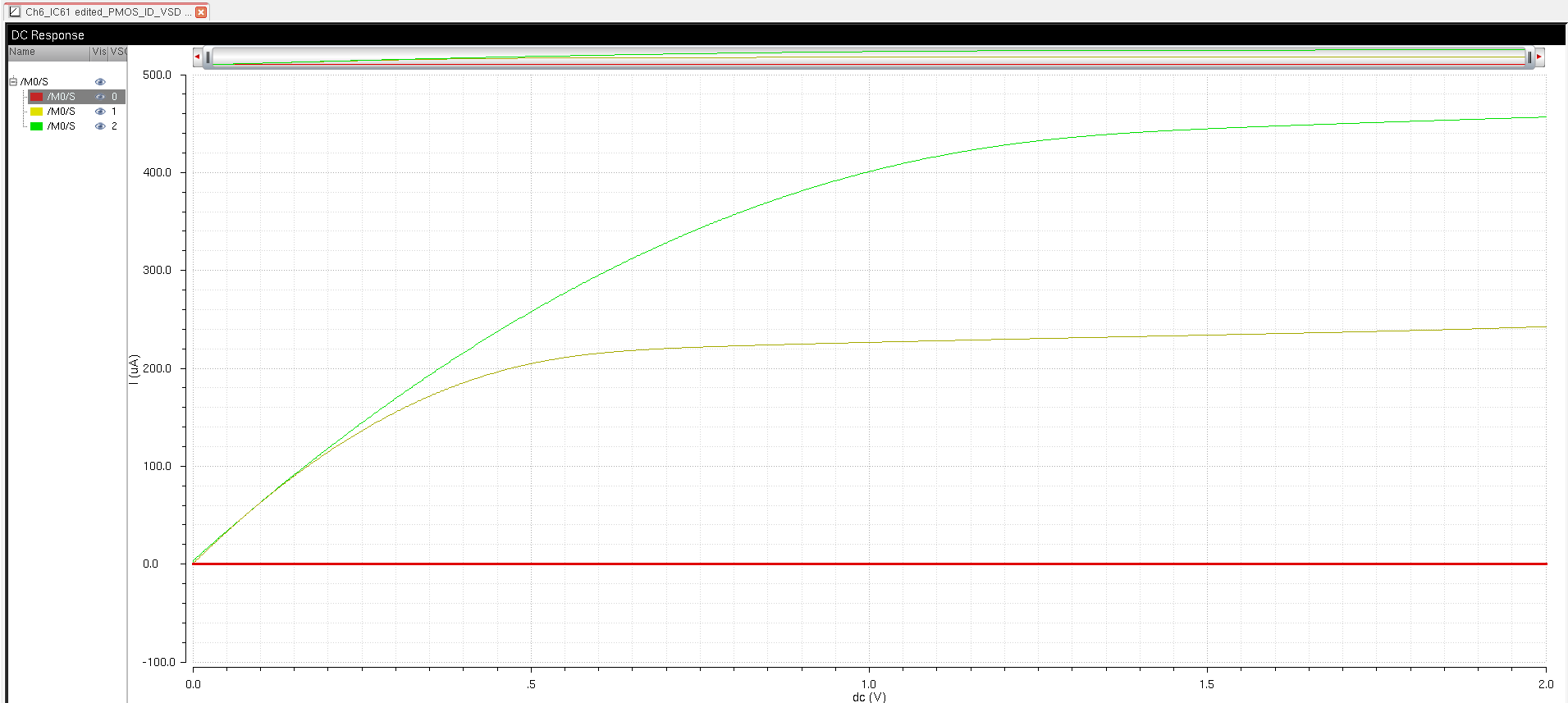
I created the schematic and simulation for the ID v. VSG of a PMOS where
VSD=100mV and VSG varies from 0 to 2V in 1 mV steps.
The PMOS dimensions are the same as the third schematic and simulation.
2)
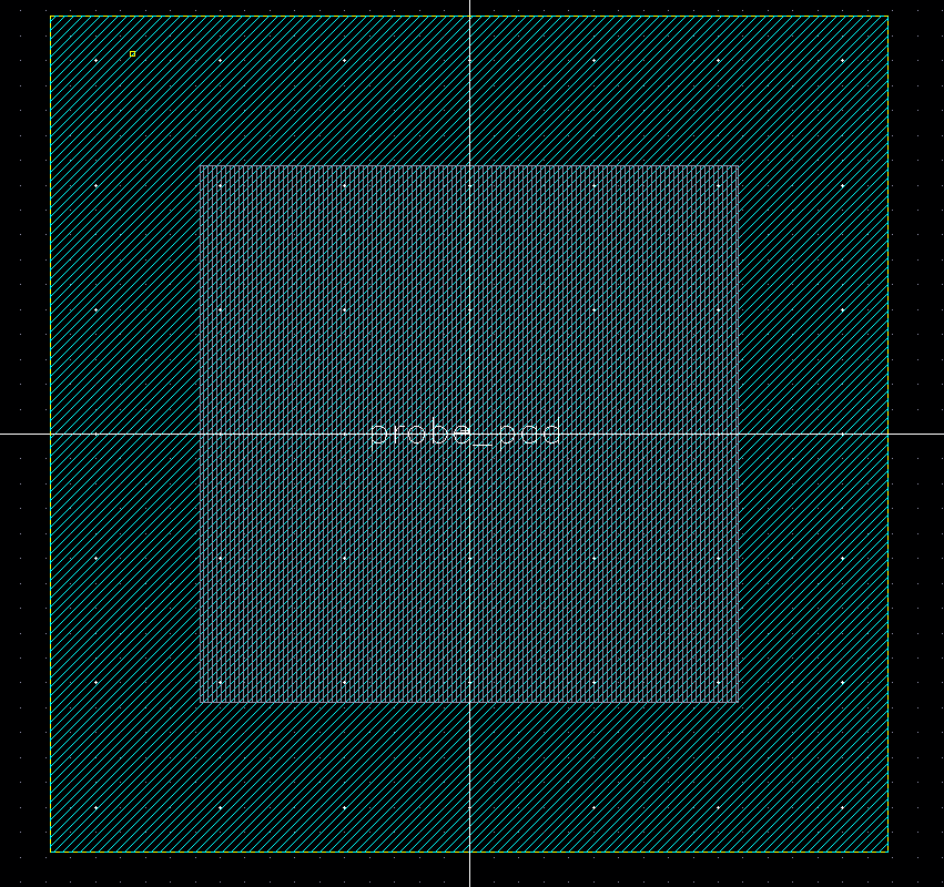
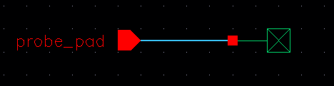
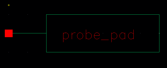
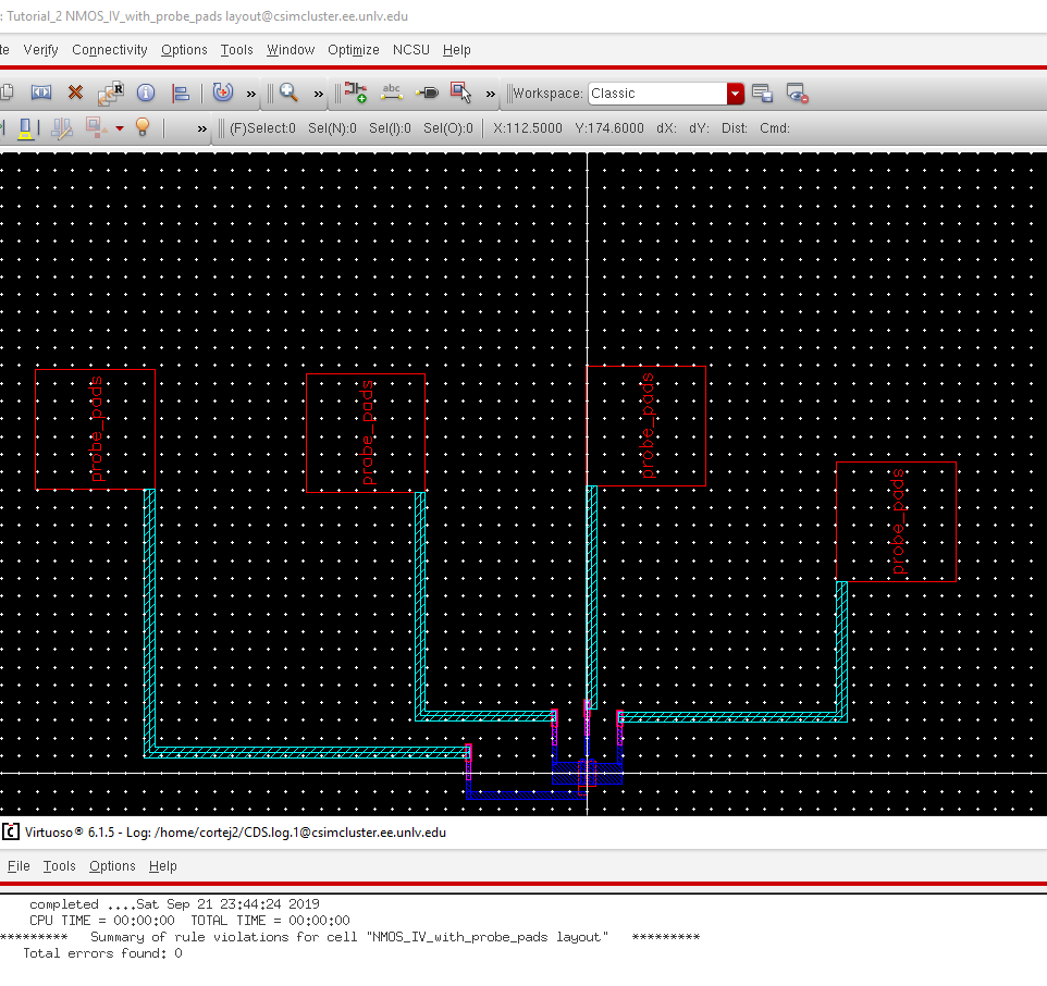
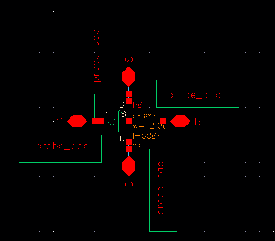
To make the NMOS from the prelab be measurable, it needs probe pads which I created in a layout, schematic, and symbol view.