Lab 3 - ECE 421L
In this lab, I applied the resistors I made in tutorial 1 to recreate the the DAC I created in lab 2.
I also discuss how to determine the width and length from MOSIS using the SCMOS_SUBM
compatible mappings.
Prelab 3:
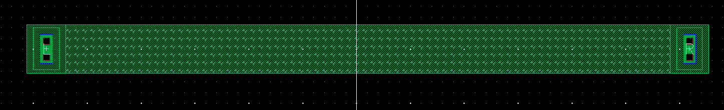
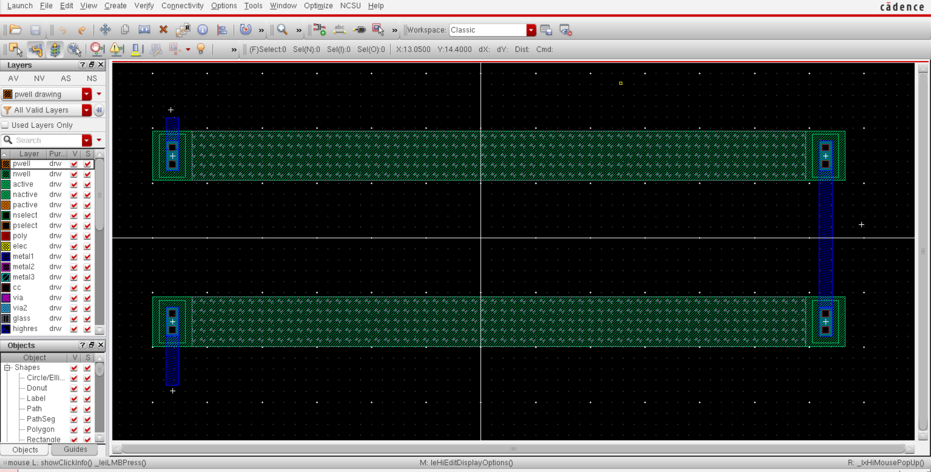
I have gone through the steps of tutorial 1, below is the layout of the resistor voltage divider.
Lab 3:
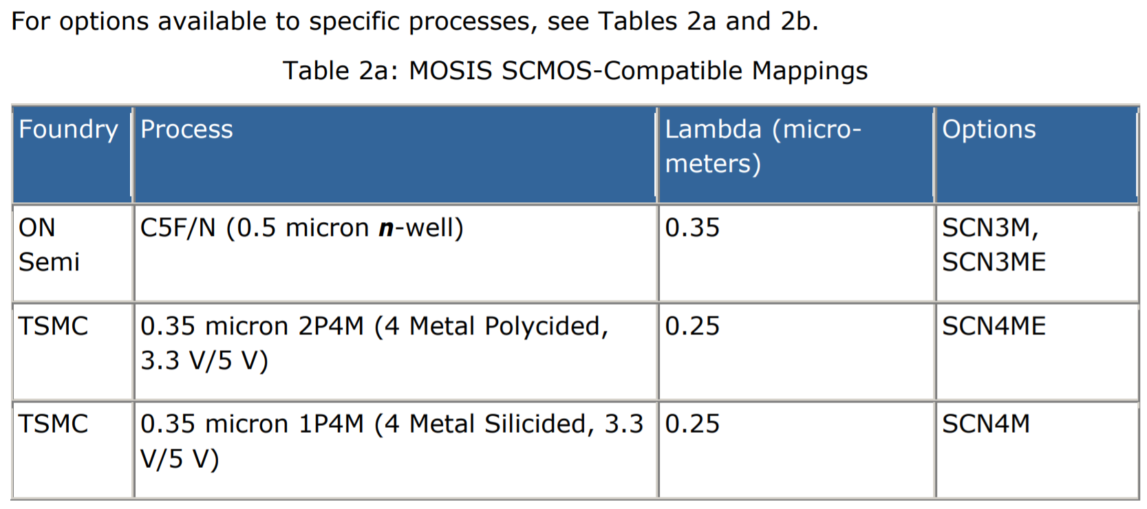
how to select the width and length of the resistor?
start
by referencing the process information from MOSIS. The references for
the process information from mosis are shown below.
They
outline they outline the scale of design, which is relative to the
process. In class we use the C5 process with a lambda of 0.30
microns.
Well width is also defined in the mosis page
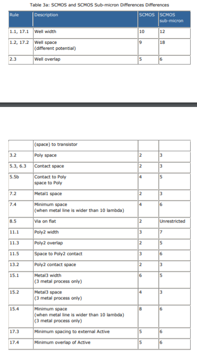
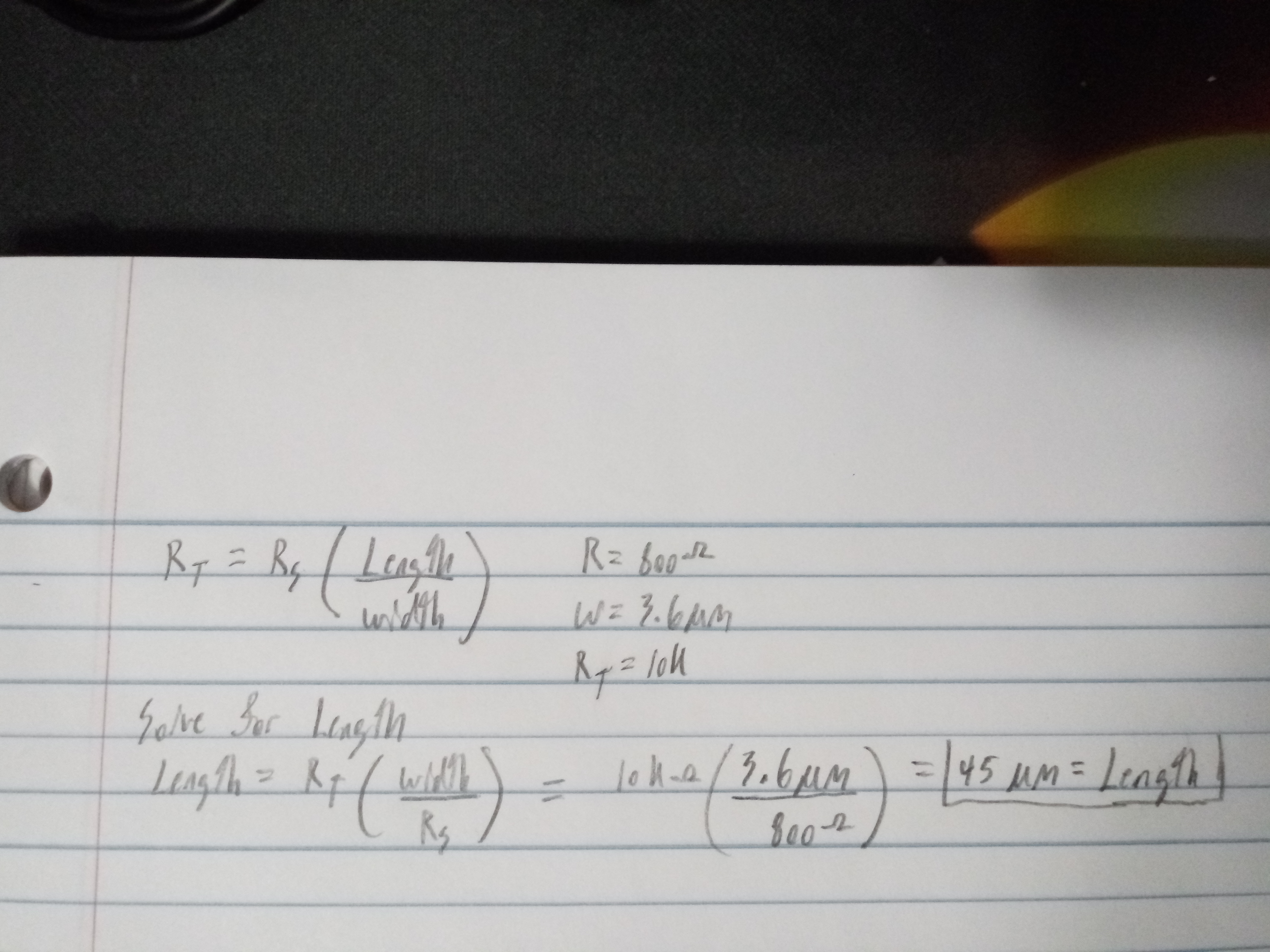
The calculations for width and length are shown below. They outline how to solve for the length of the n-well given the square resistance, width, and total resistance desired.
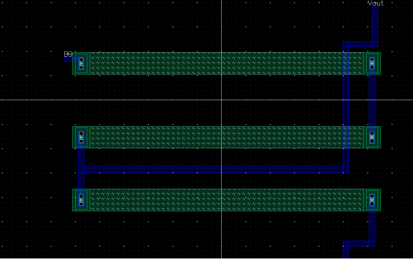
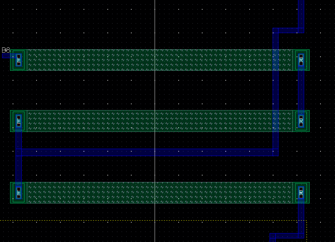
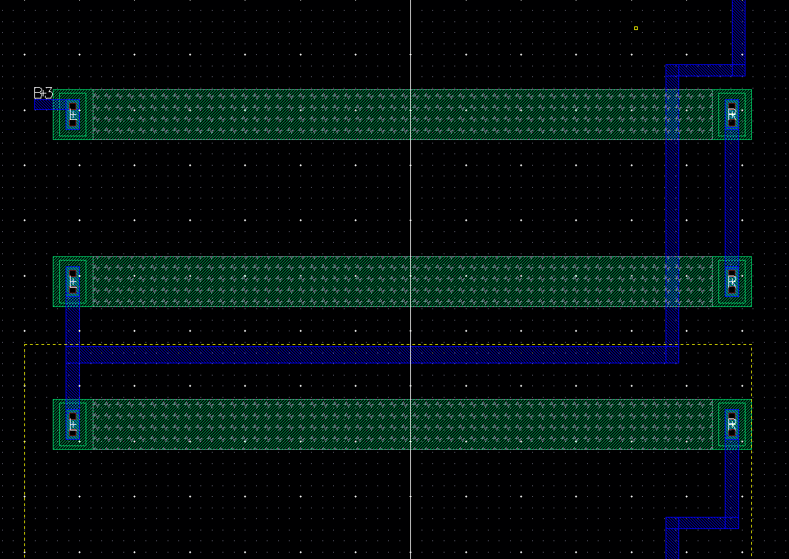
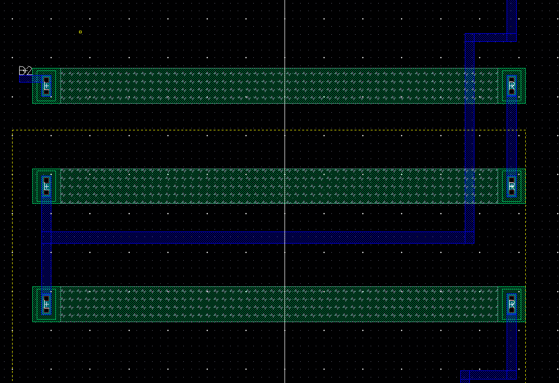
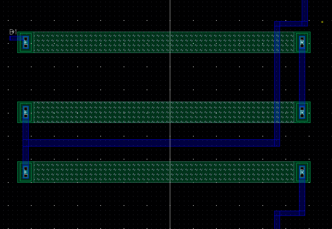
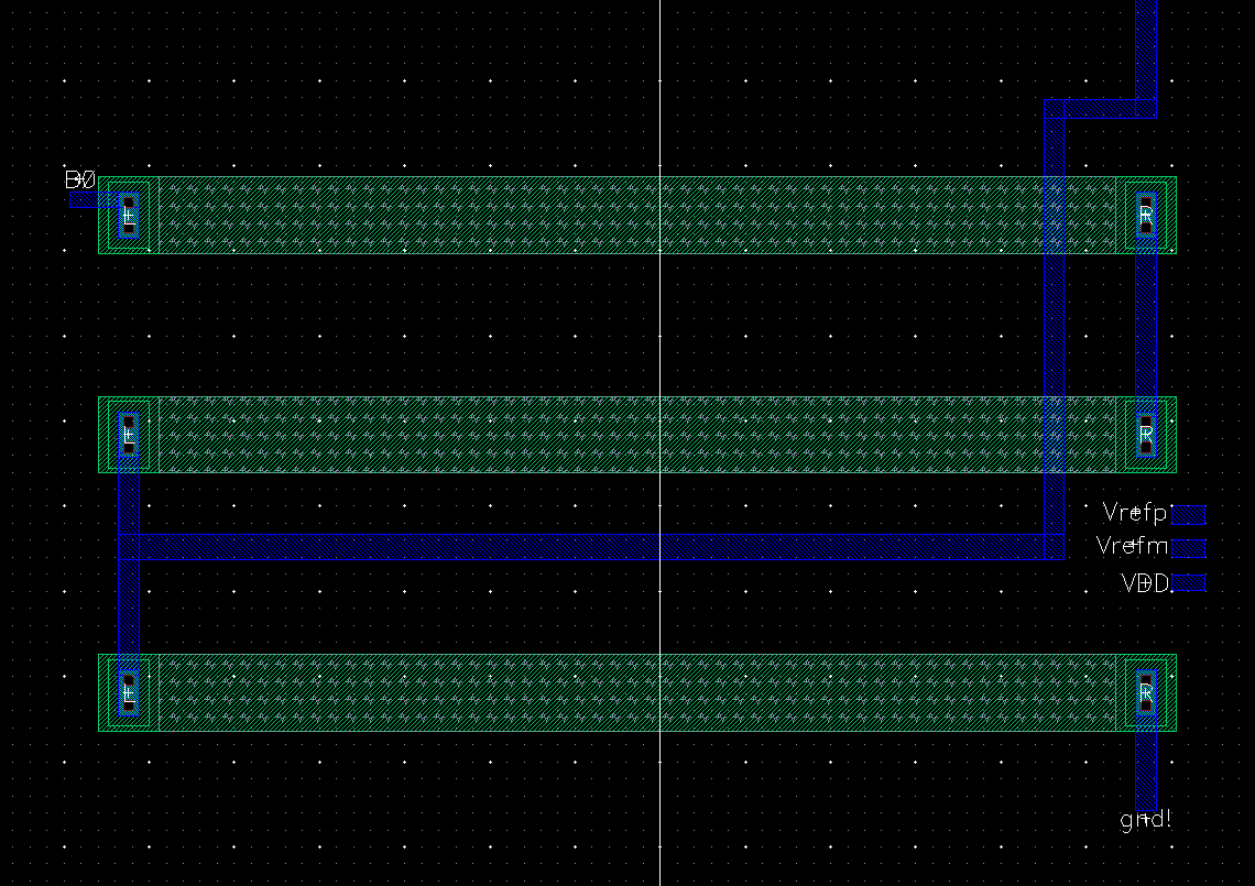
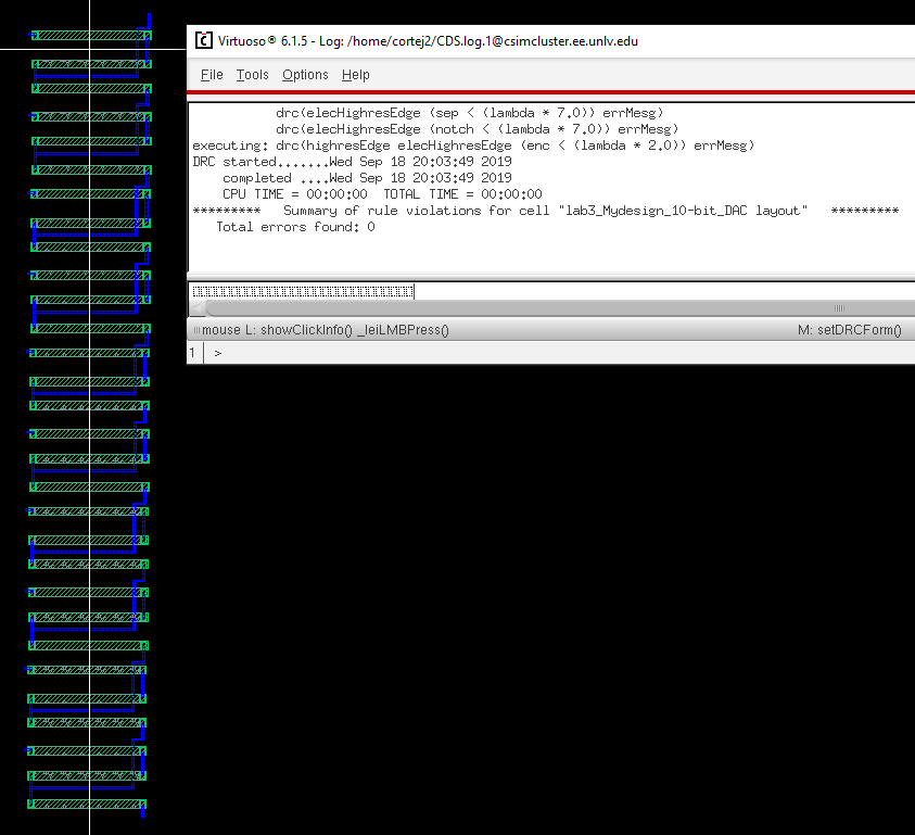
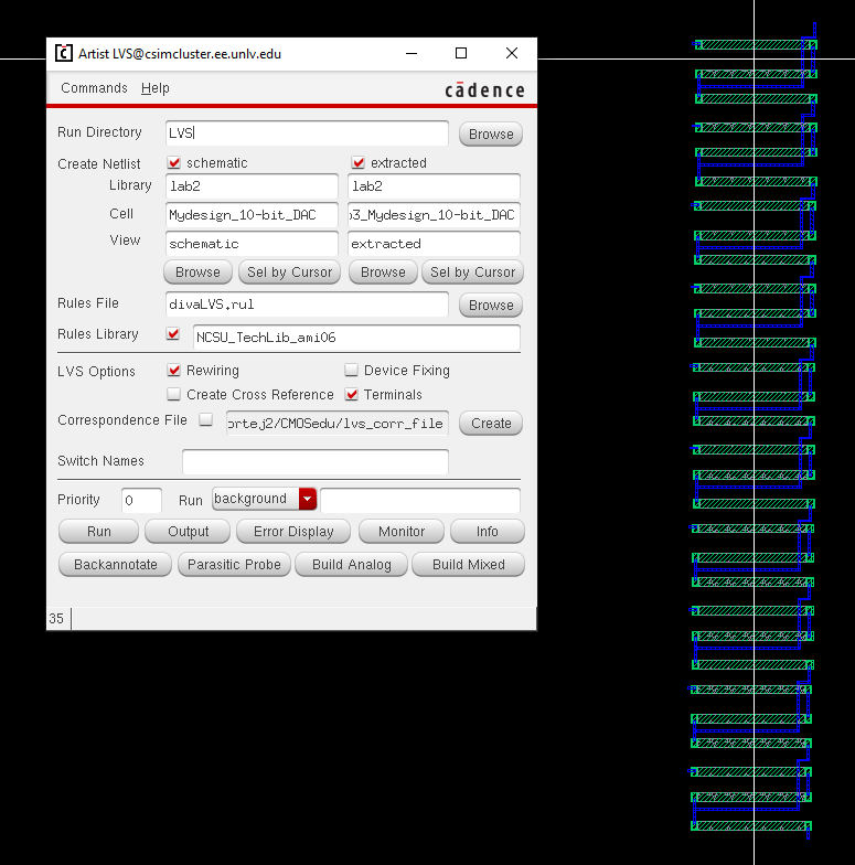
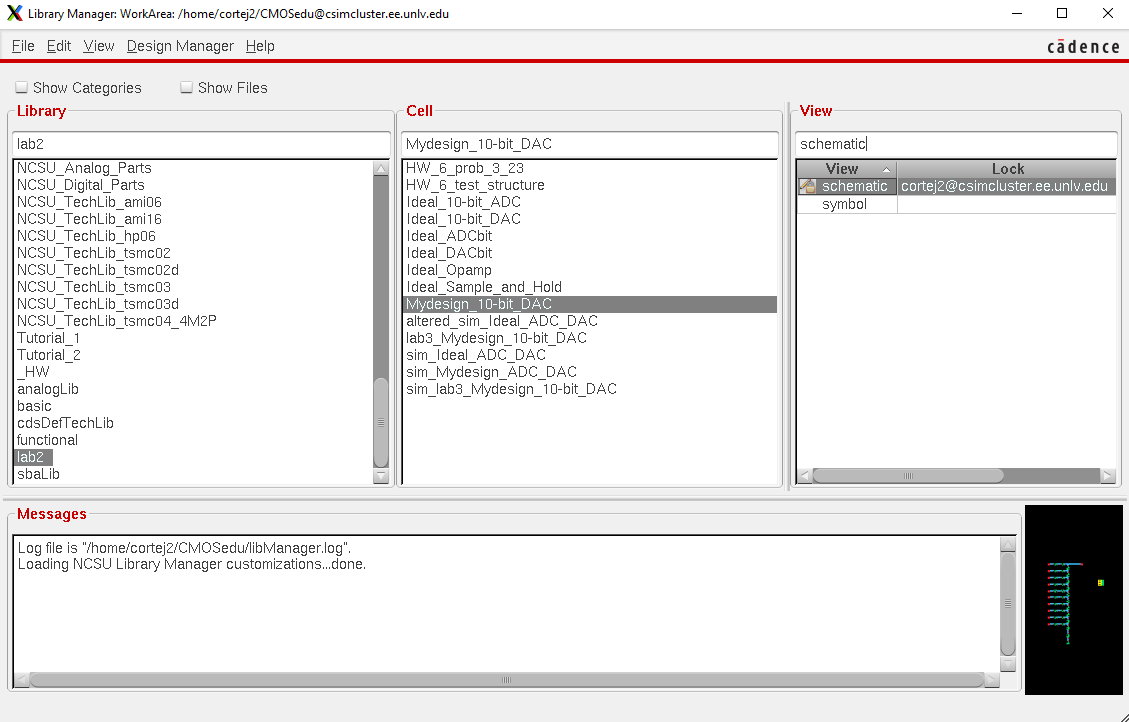
I then opened the schematic of the DAC I created in lab #2 as shown below.
I am using the lab2 folder since I will be using the schematic I made for lab#2 for this lab.
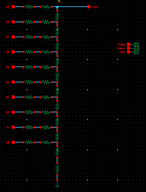
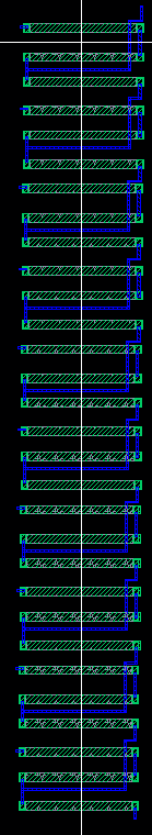
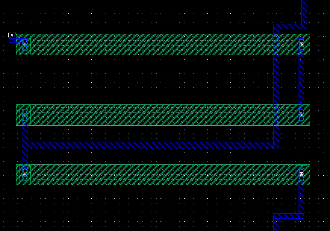
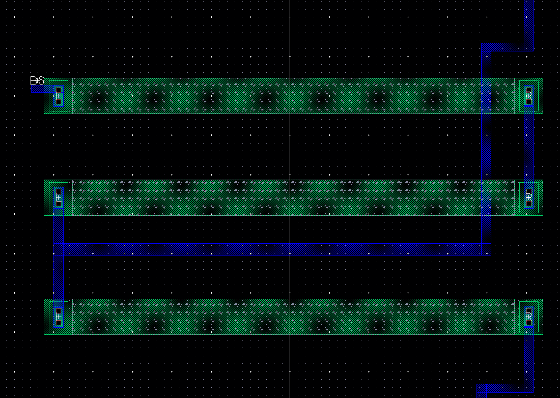
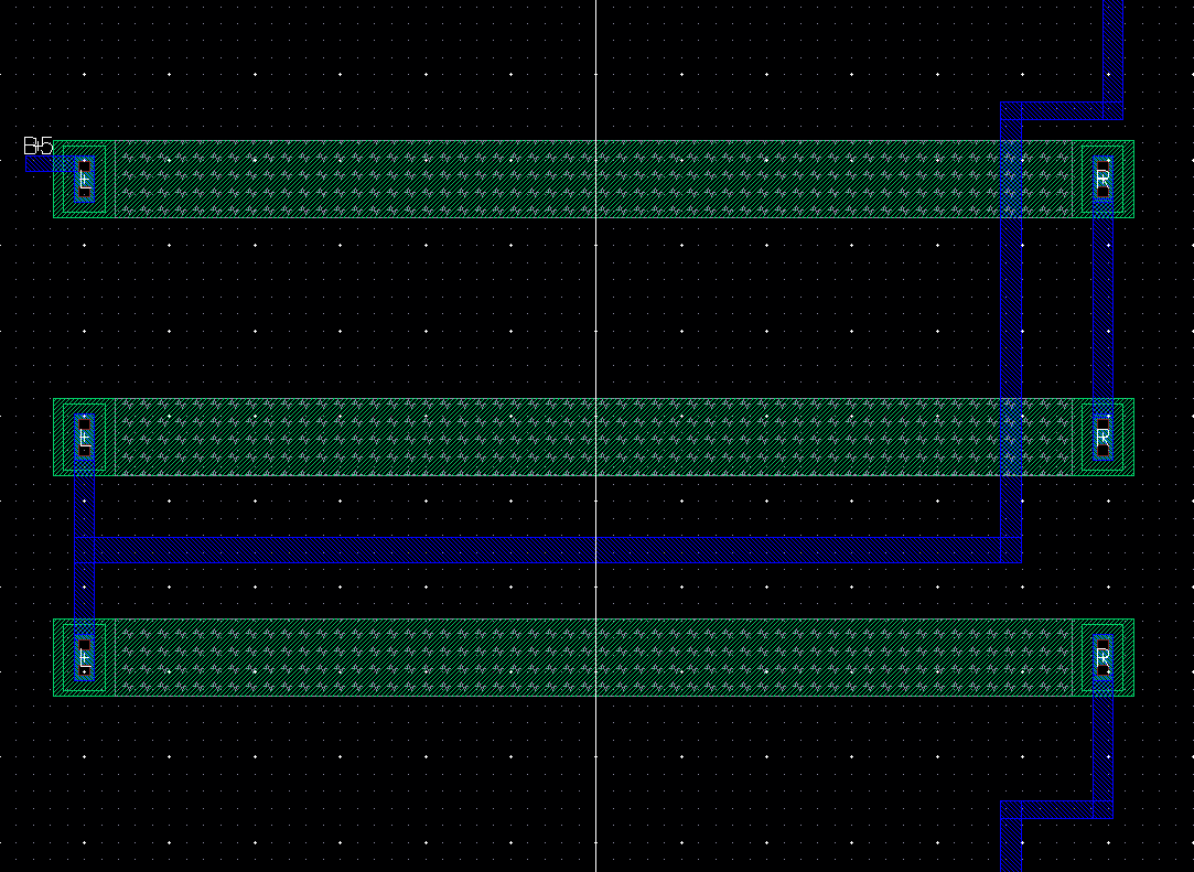
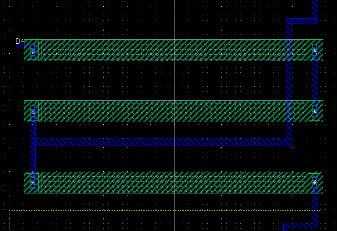
I then replaced resistors with the layout of voltage dividers I created in tutorial 1.
Layout of one resistor and the entire DAC are shown below