
Lab 2 - ECE 421L
Prelab (parts 1-3)
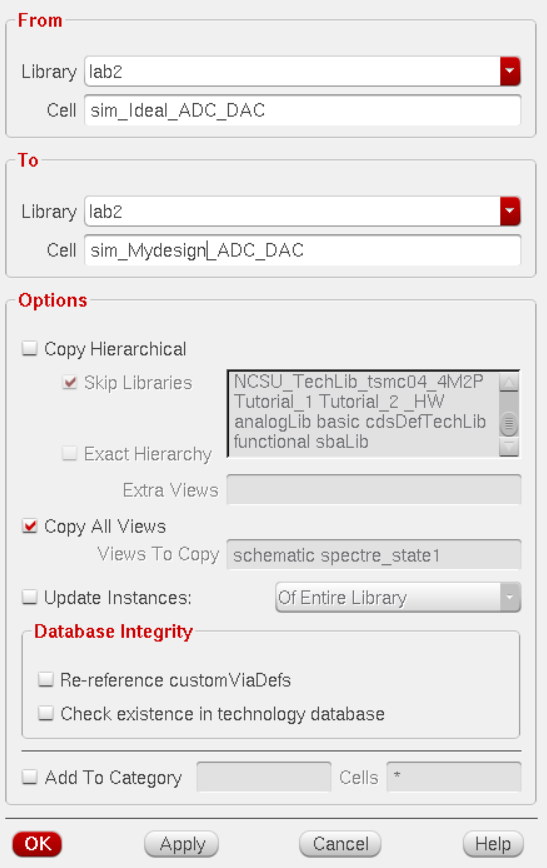
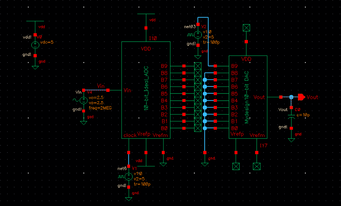
Part 1)
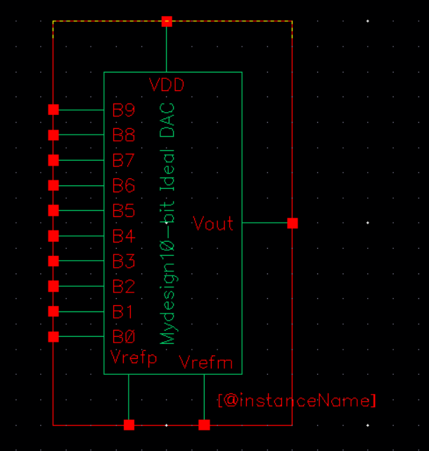
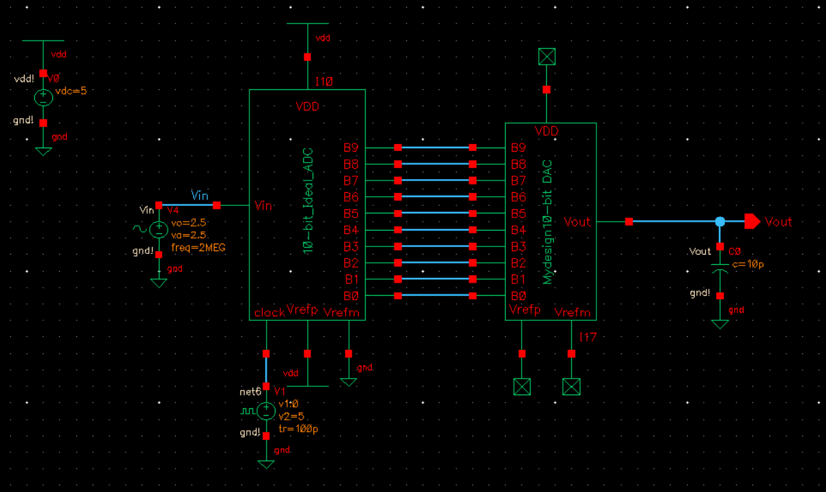
locate and simulate the ideal ADC to DAC schematic given to us on the lab 2 webpage.
The file should be located in the lab 2 file as shown below.
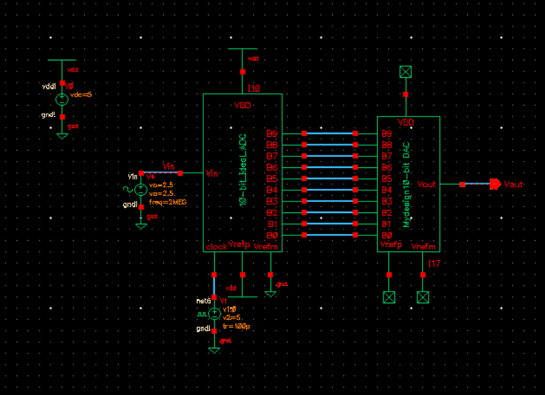
Below is how the schematic should look like.


Part 2)
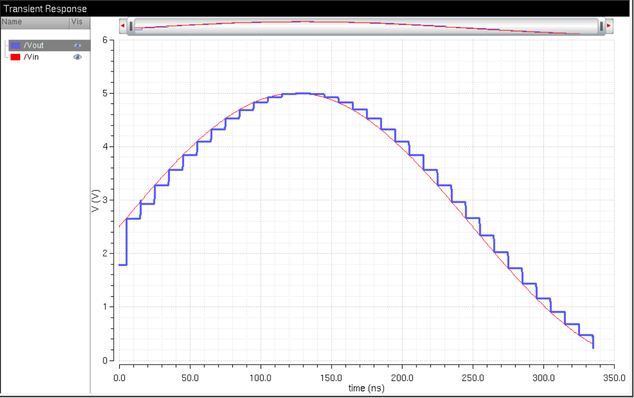
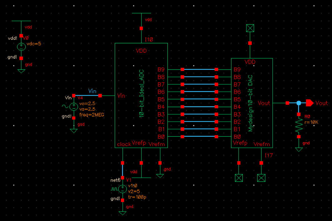
I removed the lower wires (less significant bits) connected to the 10_bit_ideal_DAC, this will cause the lesser significant bits to not be received by the DAC. The ADC will only be able to deliver the higher bits (the three most significant bits) to the DAC, the rest of the bits will still be viewable in the simulation to observe their behavior..
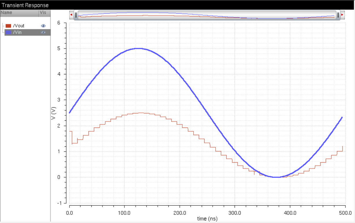
The DAC will still output a signal similar to the input signal, but since it is missing the lesser significant bits, it will appear less accurate.
The more significant bits represent the most amount of voltage in the signal. The most significant bit representing the highest amount of voltage among the other bits.
The lesser significant bits represents the smaller changes in the input signal,they represent smaller amounts of voltage, since they are removed, the output signal will be missing the smaller changes and appear less accurate when compared to the input voltage(less smooth).
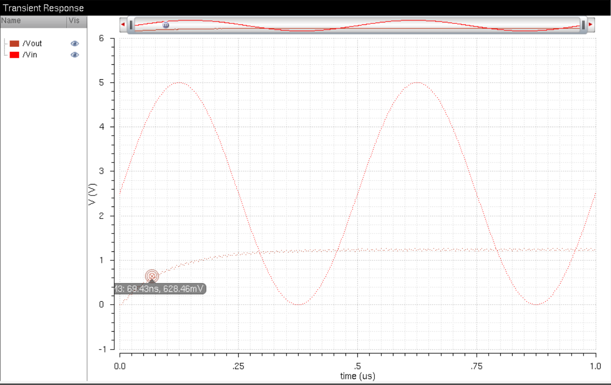
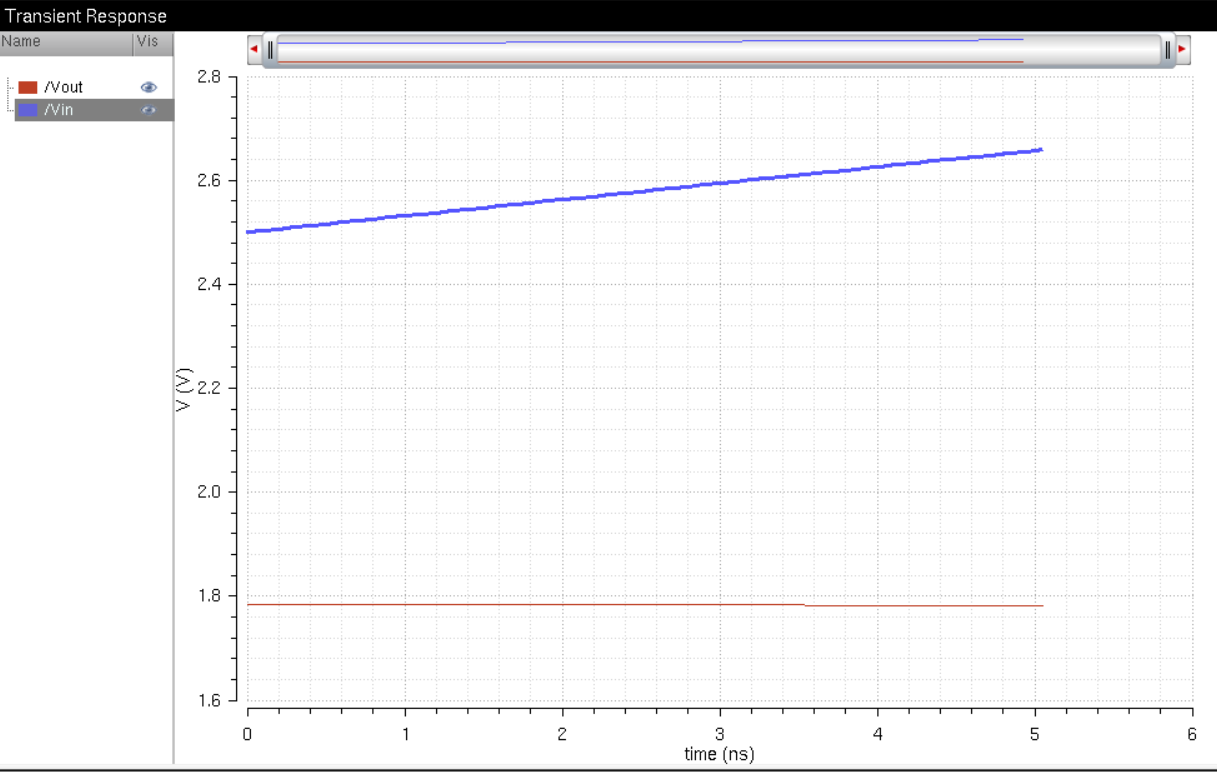
The simulation results include Vin,Vout and the lesser bits not received by the DAC. Everytime one of the lesser bits is on, there would be a small amount of voltage applied to vout to make it more similar to vin.
Below is the altered schematic and simulation results.


Part 3)
How to determine least significant bit from the converter:
The least significant bit is the one that contributes to the smallest amount of voltage change.
This can be identified by looking at when it should be on, such as simulation results like the one
shown above. It should be ON (a value of 5V) when there are small changes to the input.
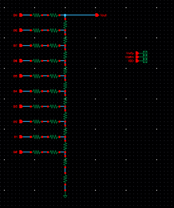
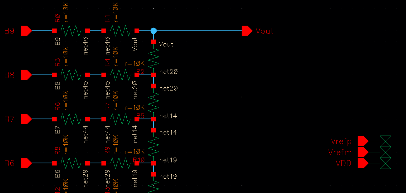
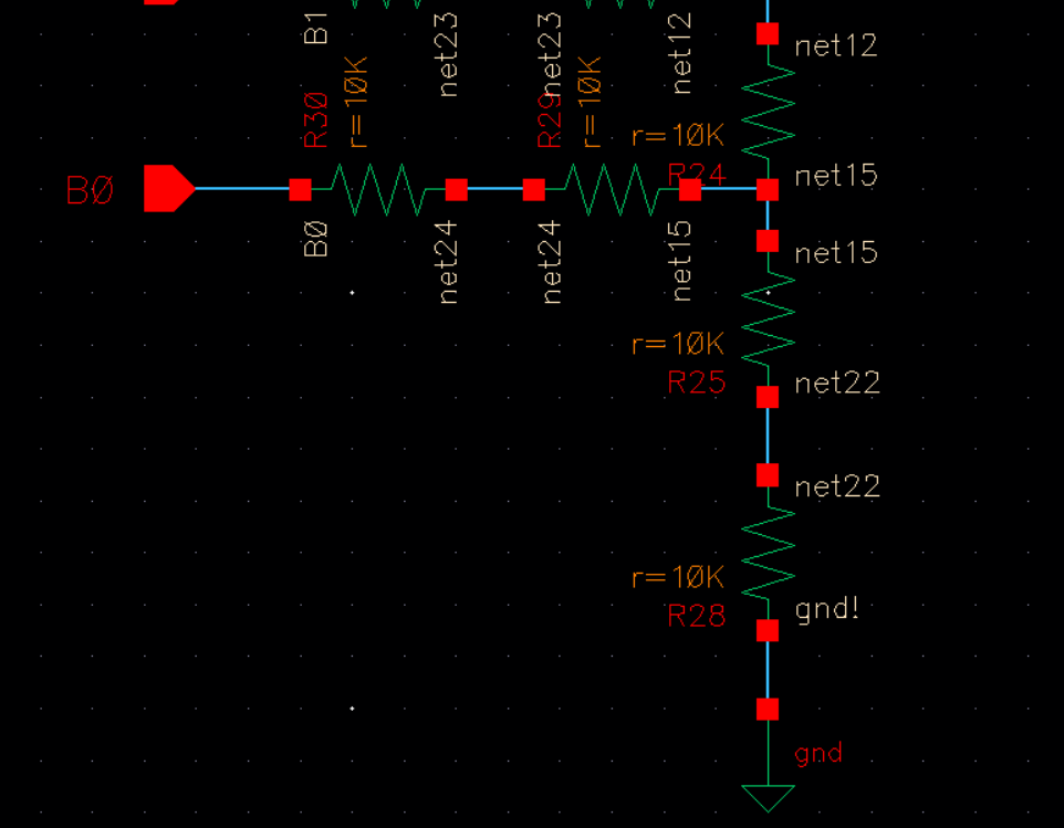
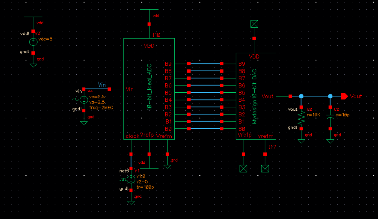
I reconfigured the ideal DAC so that it may consist of resistors (as shown below)
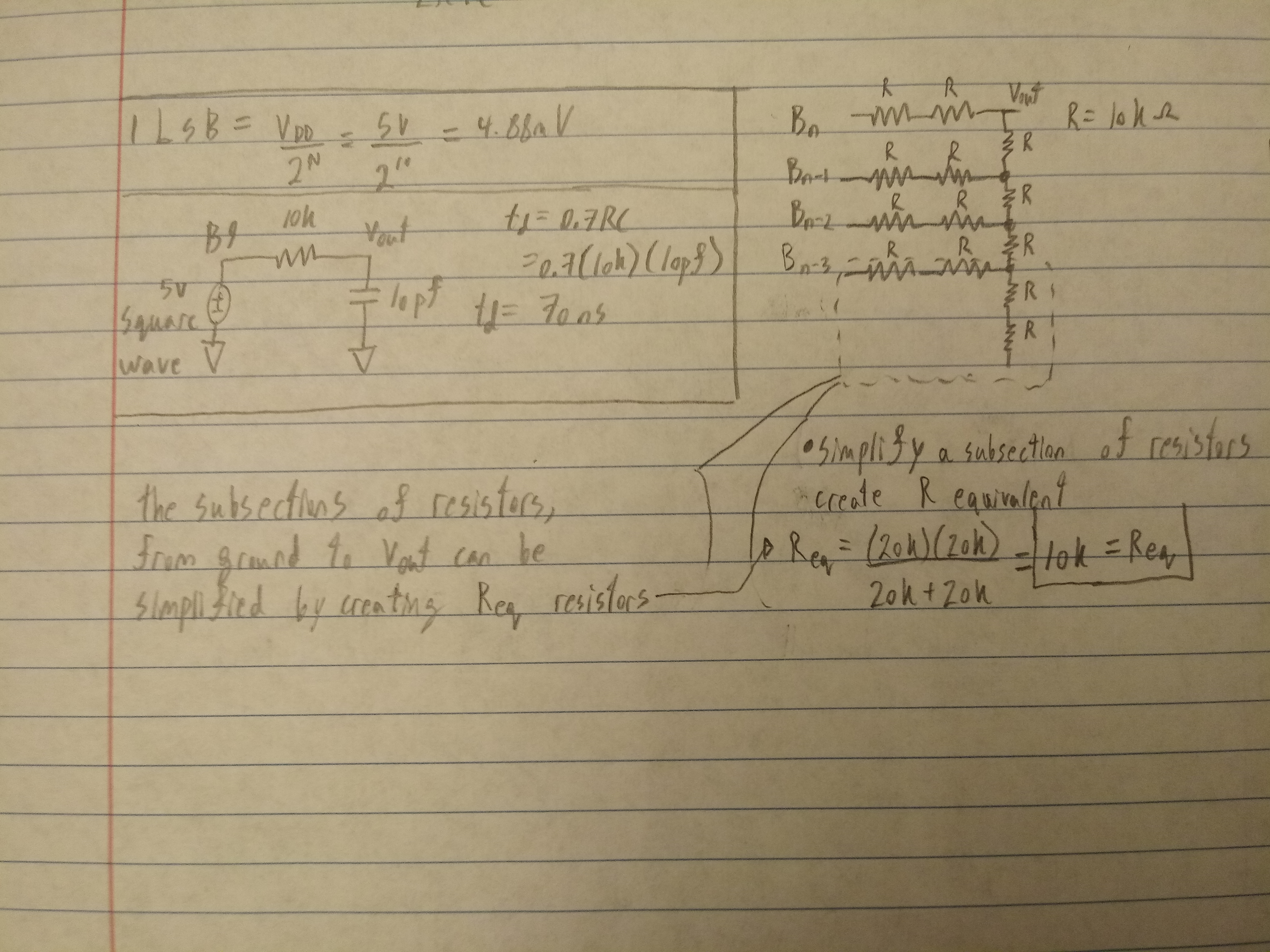
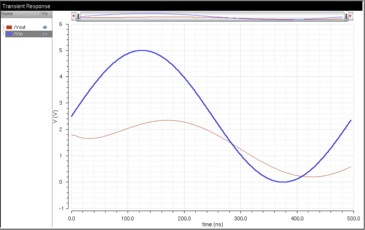
Finally, I ran a simulation with a resistive and capacitive load
-What if the resistance of the switches of the DAC (shown below) aren't small?

If the resistance of the switches were not small compared to R, then it would decrease
Vout. In every subsection of the DAC (in between nodes) there is a smaller output
proportional to Vout. The smaller outputs are Vout*1/2,Vout*1/4,Vout*1/16 and
so forth. increasing the resistance of the switches changes these propotional smaller
outputs and would thus reduce Vout. Having more voltage drops would mean the output
voltage gets reduced.