EE 421L – Digital IC
Design Lab - Lab 8
Authored by Chris Barr, Darryl Derico, Shaquille
Regis
Email: barrc1@unlv.nevada.edu, derico@unlv.nevad.edu, regis@unlv.nevada.edu
12/04/19
Zip File
lab8.zip
Lab Description:
This lab was a
compilation of everything we learned over the semester. On the pad frame built from
the beginning of the class, we instantiated multiple concepts we have covered
in the lab, as well as multiple projects from both the lab and the lecture.
Prelab
Tutorial 6:
Created the pad using 120um x 120um sizing of the pad layer. Followed by
a 75um x 75um metal3 layer and a 63um x 63um glass layer on top.
Tabulated Designs of the Pad:
|
Schematic |
Symbol |
Layout |
|
|
|
|


With the acquired pad layout, the construction of the pad frame may begin.
There will be 10 pads on each side.
The pad layer creates a 45um spacing in between each pad.
Tabulated Designs of the Pad frame:
|
Schematic |
Symbol |
Layout |
|
|
|
|


The chip is ready to be constructed, given the pad frame is put together properly. A design can be placed
onto the pad frame, as seen below.
Tabulated Designs of the Chip:
|
Schematic |
Layout |
|
|
|


This concludes Tutorial 6
Lab
Objective: Create a chip layout containing these components.
1.
PMOS
2.
NMOS
3.
Voltage Divider
4.
Ring Oscillator
5.
Inverter
6.
NAND Gate
7.
NOR Gate
8.
Boost SPS
9.
x4 Clock Multiplier
10. Pad Frame
This is the main schematic for the chip. Every component listed above is
on this figure.

Fig. 1 Chip Schematic

Fig. 2 Chip Schematic Pin Names in order
Pad Frame
The pad frame is the skeleton of the chip. It consists of 40 pads that
can be used for multiple terminals. The pads are labeled
1 through 40 starting from the top pad on the right
side of the chip, and increments clockwise ending with pad 40 on the rightmost
pad at the top of the chip. Pads 30 through 40 are not
connected to anything. All involved schematics have a common
ground placed on pad 8. The connections were set in a way that would mostly
separate the various terminals intended for an input voltage.
Reference Fig. 1 and Fig. 2 for the designated pin connections and descriptions.
PMOS
Schematic & Layout of the PMOS:

Fig. 3 PMOS Schematic

Fig. 4 PMOS Layout
Testing this
device:
The relevant PMOS terminals are pads 1 through 4 and are referenced
as PM<1:4> on the schematic. You would supply the gate voltage
to pin 2, the drain voltage to pin 3, the source
voltage to pin 1, and the body voltage to pin 4.
NMOS
Schematic & Layout of the NMOS:

Fig. 5 PMOS Schematic
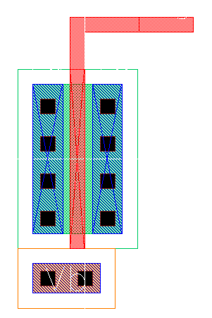
Fig. 6 PMOS Layout
Testing the Device:
The relevant NMOS terminals are pads 5 through 7 and are referenced as NM<5:7> on the schematic. You would supply the gate voltage
to pin 6, the drain voltage to pin 5, and the
source voltage to pin 7.
Voltage Divider
Schematic & Layout of the Voltage Divider:

Fig. 7 Voltage Divider Schematic

Fig. 8 Voltage Divider Layout
Testing the Device:
The relevant Voltage Divider terminals are pads 9 through 10 and are referenced
as VD<9:10> on the schematic. You
would supply the input voltage through
pin 10 and read the output from pin 9.
Ring Oscillator
Schematic & Layout of the Ring Oscillator:

Fig. 9 Ring Oscillator Schematic

Fig. 10 Ring Oscillator Layout
Testing the Device:
The relevant Ring Oscillator terminals are pads 11 through 12 and are referenced
as RO<11:12> on the schematic.
You would supply the input voltage to pin 11, and read the output signal
resulting from the buffer from pin 12.
Inverter
Schematic & Layout of the Inverter:

Fig. 11 Inverter Schematic

Fig. 12 Inverter Layout
Testing the Device:
The relevant Inverter terminals are pads 13 through 15 and are referenced
as INV<13:15> on the schematic.
You would connect the source voltage or
VDD to pin 15, the inverter input to pin 13, and read the output of the
inverter from pin 14.
NAND Gate
Schematic & Layout of the NAND Gate:

Fig. 13 NAND Gate Schematic

Fig. 14 NAND Gate Layout
Testing the Device:
The relevant NAND Gate terminals are pads 16 through 19 and are referenced
as NAND<16:19> on the schematic.
You would connect the source voltage or VDD to pin 19, the inputs of the
NAND gate to pin 16 and pin 17, and read the resulting signal from pin 18.
NOR Gate
Schematic & Layout of the NOR Gate:

Fig. 15 NOR Gate Schematic

Fig. 16 NOR Gate Layout
Testing the Device:
The relevant NOR Gate terminals are pads 20 through 23 and are referenced
as NOR<20:23> on the schematic.
You would connect the source voltage or VDD to pin 23, the inputs of the
NOR gate to pin 20 and 21, and read the resulting signal from pin 22.
Boost SPS
Schematic & Layout of the Boost SPS:

Fig. 17 Boost SPS Schematic

Fig. 18 Boost SPS Layout
Testing the Device:
The relevant Boost SPS terminals are pads 24 through 26 and are referenced
as SPS<24:26> on the schematic.
You would connect the source voltage or VDD to pin 26, connect one end
of the off-chip inductor and anode of the off-chip Schottky
diode to pin 25, and connect the cathode of the off-chip Schottky
diode, off-chip resistor, and off-chip capacitor to Vout.
x4 Clock Multiplier
Schematic & Layout of the x4 Clock Multiplier:

Fig. 19 x4 Clock Multiplier Schematic

Fig. 20 x4 Clock Multiplier Layout
Testing the Device:
The relevant x4 Clock Multiplier terminals are pads 27 through 29 and are referenced as CM<27:29> on the schematic. You would connect the source voltage or VDD to pin 29, and the clock to
be multiplied to pin 27. The resulting multiplied clock
can be read from pin 28.
Chip Verification

Fig. 21 Chip Layout

Fig. 22 Chip DRC Verification

Fig. 23 Chip LVS Verification
Return to
Darryl Derico’s Labs