The goal of this project is to create an 8-bit serial-to-parallel converter. The following content will document the creation of schematics, layouts, and simulations for this converter.
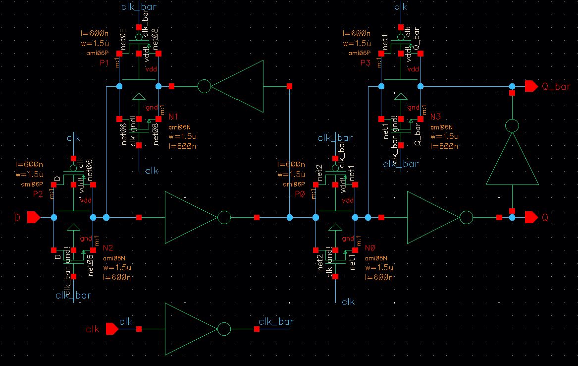
In order to draft the schematic for the serial-to-parallel converter, we must first create the schematic and symbol for a D flip-flop. The schematic drafted can be seen below:
The combination of PMOS and NMOS in parallel vertically like in this schematic is known as a transmission gate, which allows for the flip-flop to "store" values when combined with inverters.
The first block on the left is known as a flow-through latch, which is a latch that stores the current value (although negated). When cascaded, this creates the D flip-flop, storing both Q and Q_bar after each edge-triggered clock cycle.
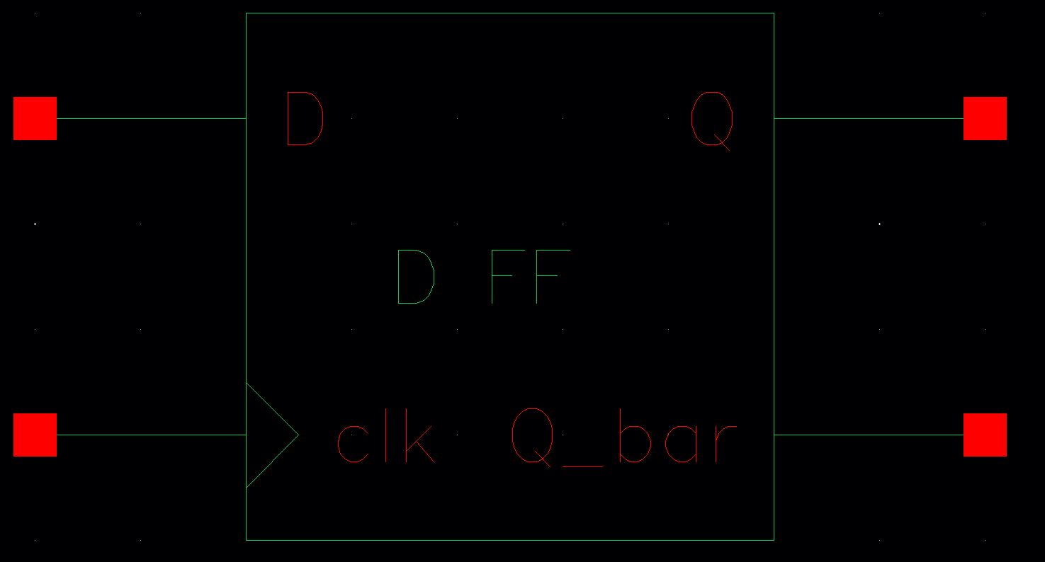
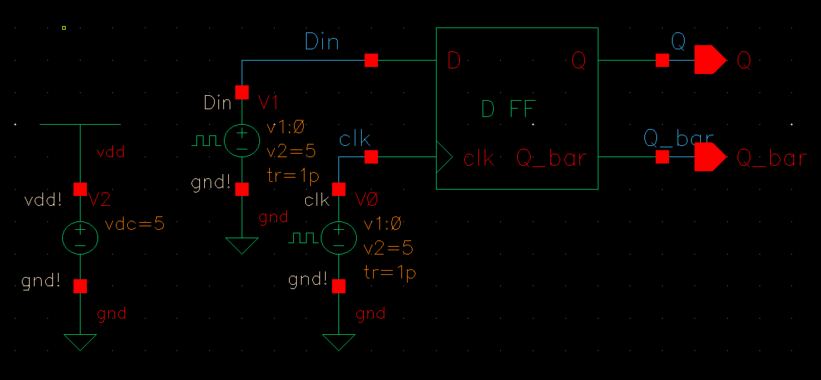
Next, we can create a schematic for the D flip-flop as seen below:
In order to draft the 8-bit serial-to-parallel converter, we will first create an 8-bit shift register. The clock of this shift register will be clock_in.
The Q of each bit in this shift register is then fed parallel into the Din of a parallel set of D flip-flops that store the current word every 8 cycles of the shift register clock. This new clock will be clock_out.
clock_out is created by cascading three D flip-flops with Q being fed into clk_in of the next flip-flop. For each flip-flop, Q_bar is fed back into Din for that flip-flop, essentially halving the rate at which clock_in transmits.
Since these 3 flip flops are cascaded this means that the new clock will be 1/(2^3) = 1/8 the freqeuncy ofour input clock.
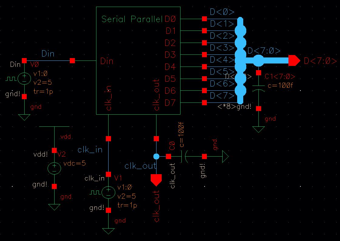
The schematic for the serial-to-parallel converter can be seen below:
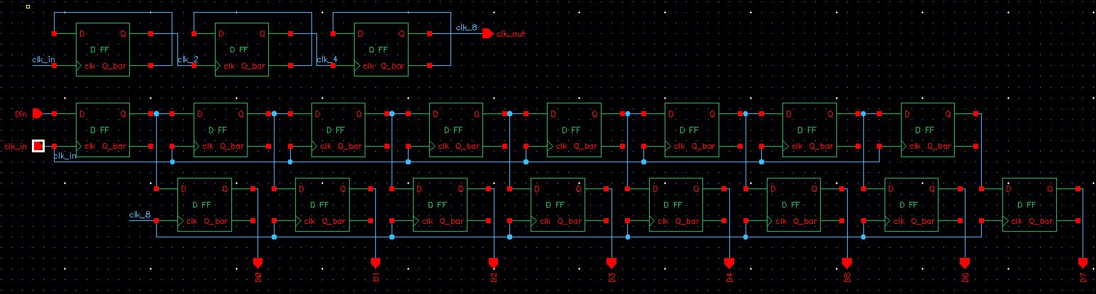
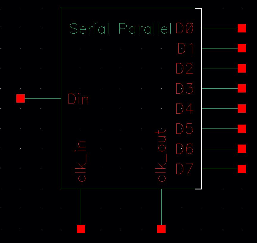
As seen in this schematic, the Q_bar output of both the shift and parallel registers are not used in our design. The symbol for the serial-to-parallel converter can be seen below:
In order to verify the design of the serial-to-parallel converter, we must create a set of simulations to test the converter's operation. The schematic for simulation can be seen below:
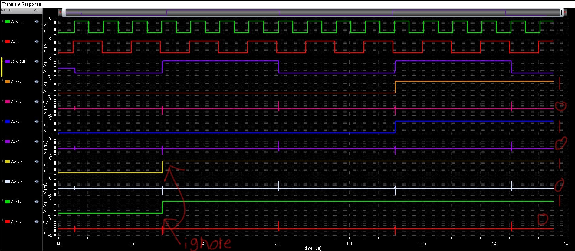
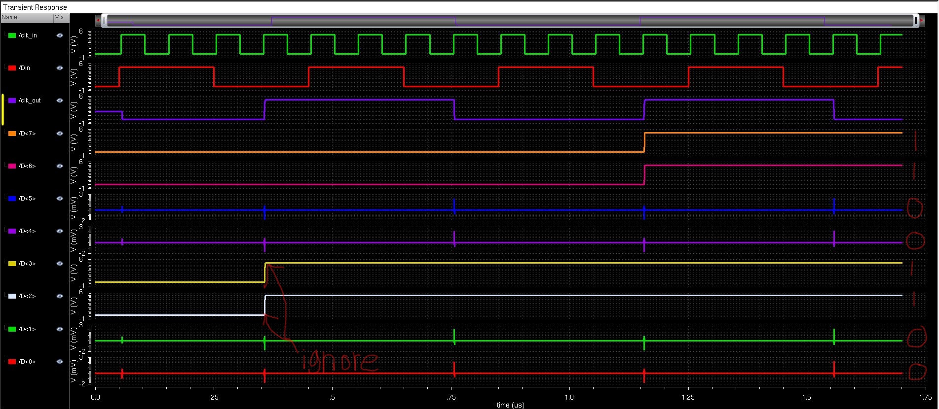
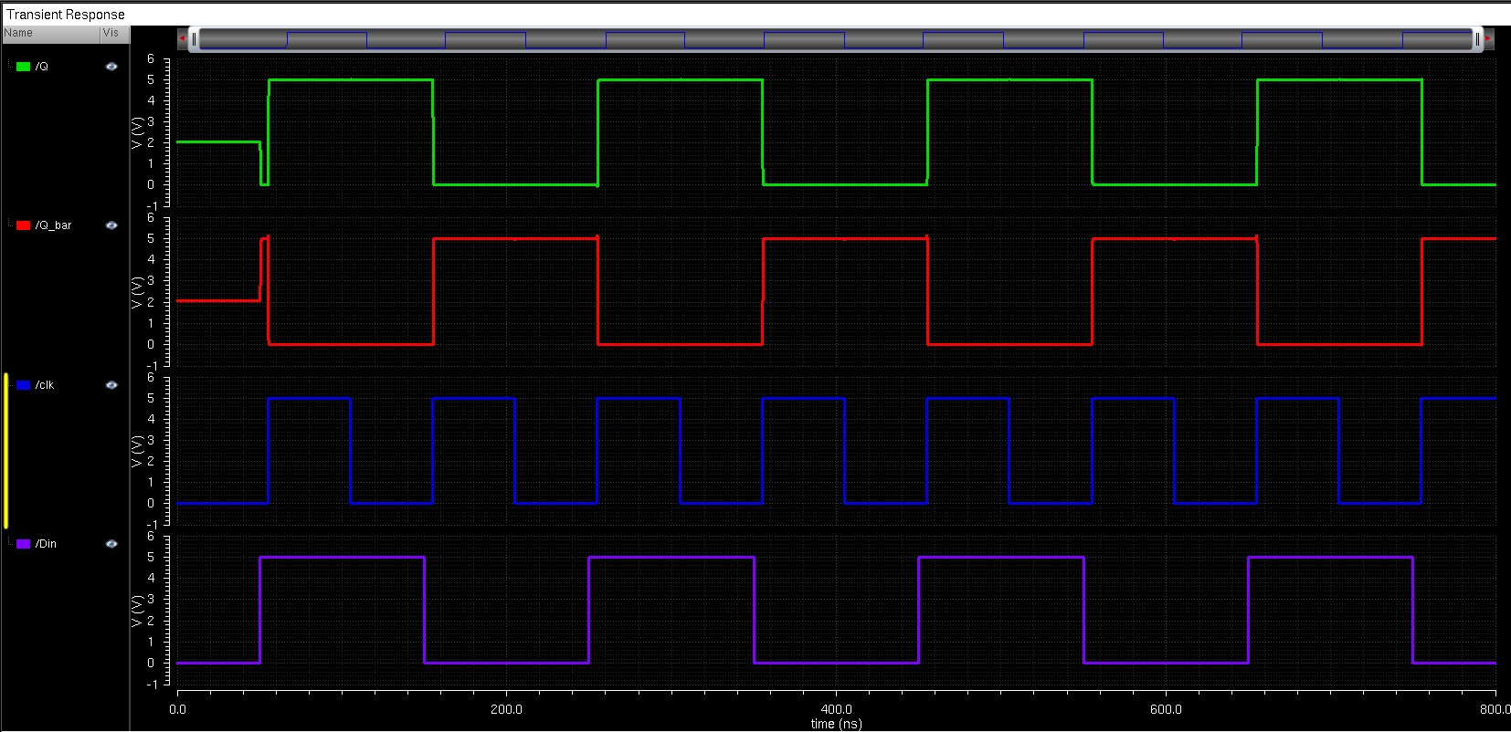
Like the previous simulation, we must ignore the first output cycle due to intial values being held in the parallel register.
Finally, note that there can be "glitches" in the output due to transistors in the D flip-flops not being ON or OFF at that point, due to the switching of the clock.
The zip file containg the schematics used in this section of the project can be found in proj_schem.zip
The layout for the D Flip-Flop can be seen below:
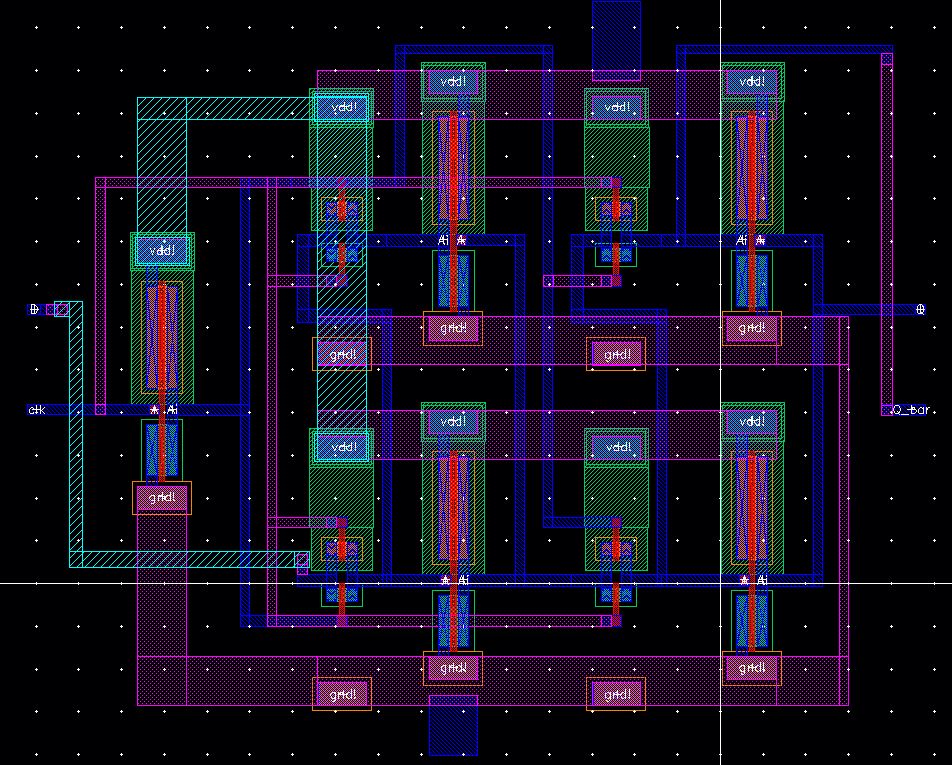
As seen here, the layout made use of the schematic to guide the routing, and multiple metals to reduce complicated paths.
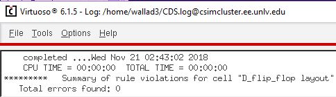
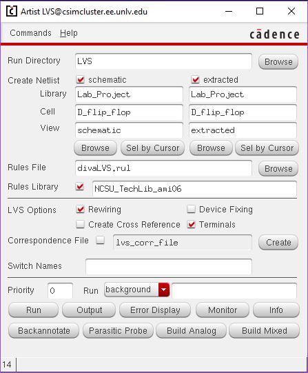
The DRC & LVS results for the D flip-flop layout can be seen below:

The layout for the serial-to-parallel converter can be seen below:
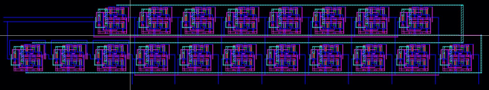
As seen in this image, ground and power buses were layed out horizontally to allow for easier connections to other objects.
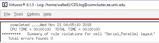
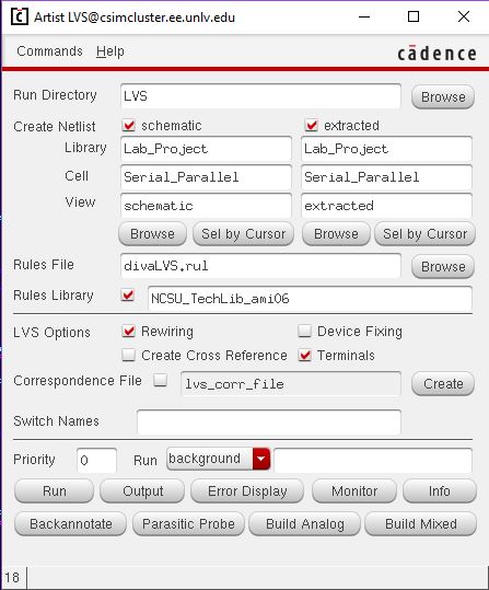
The DRC & LVS results for the serial-to-parallel layout can be seen below:

The zip file containg the schematics & layouts used in this project can be found in proj_final.zip