Lab 2 -
EE 421L
Author: Dylan
Wallace
Email: wallad3@unlv.nevada.edu
Date modified:
September 11, 2018
Lab
Description
This
lab introduces the design of a 10-bit digital-to-analog converter (DAC).
Pre-Lab
objectives
-
Run the simulation of the 10-bit ADC-DAC.
-
Understand the relationship between Vin
and Vout.
-
Provide
and discuss different simulations in order to demonstrate knowledge of
ADC and DAC operation.
- Explain how
to determine the least significant bit (LSB), with simulations to
support.
Pre-Lab
-
We will start with downloading the "lab2.zip" file from
the
EE
421L page, transferring it to MobaXterm, and unzipping the contents
into ~/CMOSedu/lab2.
-
Add the definition of the new directory into the "cds.lib"
file in ~/CMOSedu.
-
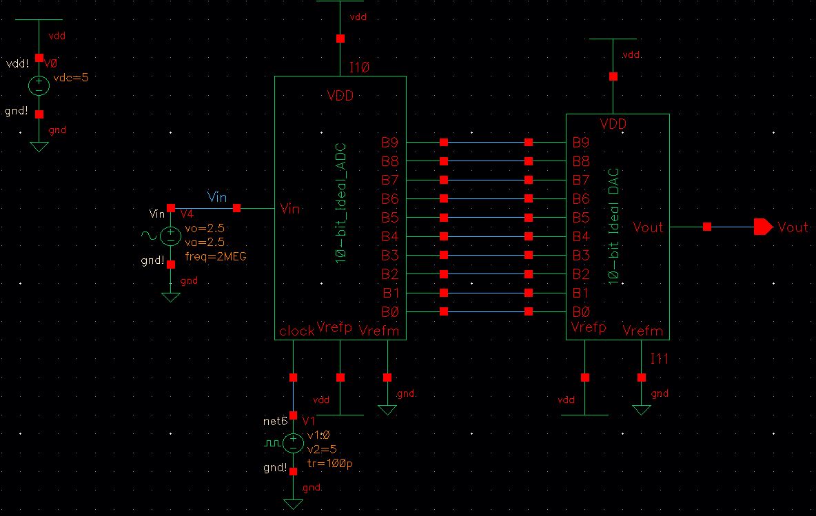
Open the schematic of "sim_Ideal_ADC_DAC". It should look
like the image below:
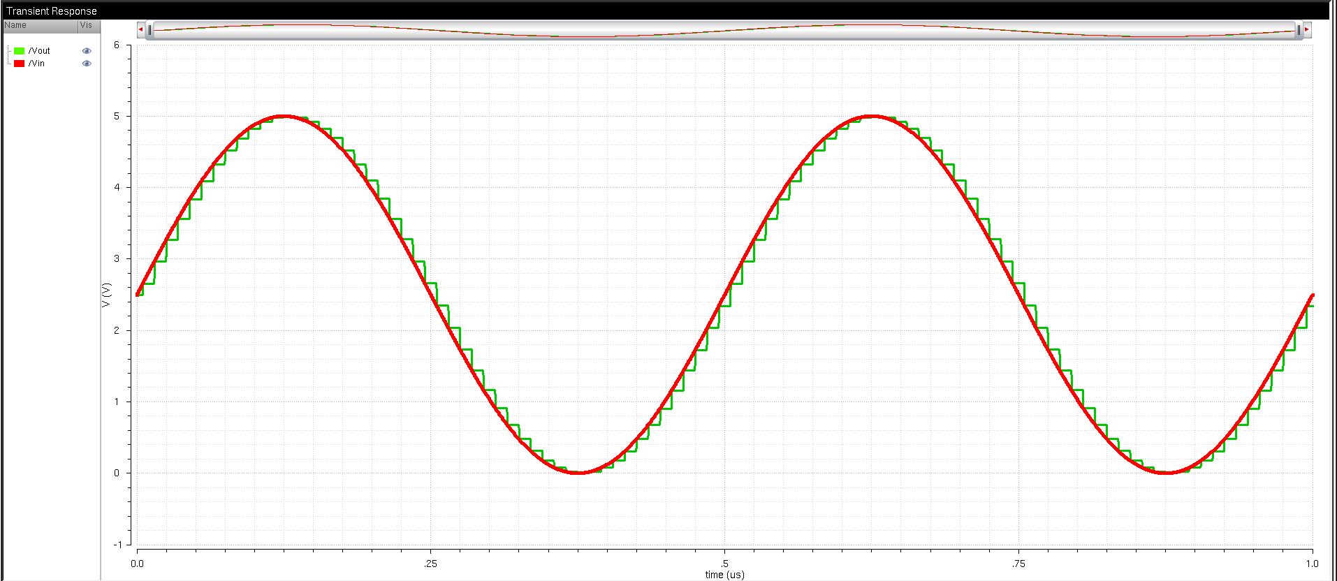
- Run the simulation by launching ADE L and loading the
"spectre_state1". Change the background to white, the Vin
trace
to a red extra thick solid line, and the Vout
trace to a green thick solid line.
Relationship Between Vin
and Vout
Vin
is an analog input signal that is fed into a 10-bit ADC and then back
through a DAC to get Vout. Therefore, Vout
is a digital representation of Vin.
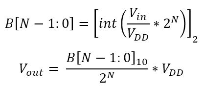
Vout can be determined using the following
equations:
Simulations to Test Knowledge
In order to more easily show the
influence of the
digital-to-analog conversion, the amplitude and offset of Vin
can be changed to 20 mV. As can be seen in the image below, the
stratification between LSBs is more significant at lower voltage levels:
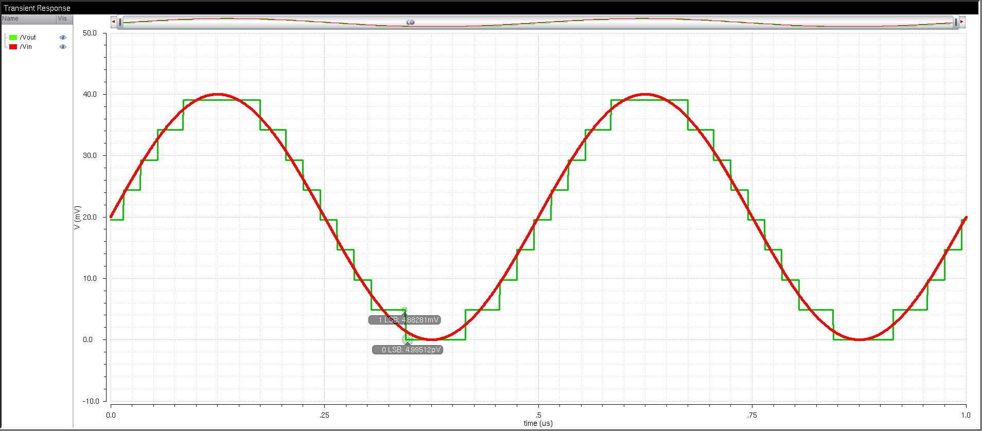
How to Determine the Least Significant Bit (LSB)
The least significant bit (LSB) can be
determined
using the equation below. For our 10-bit ADC-DAC schematic, the LSB
comes to be 4.88 mV:
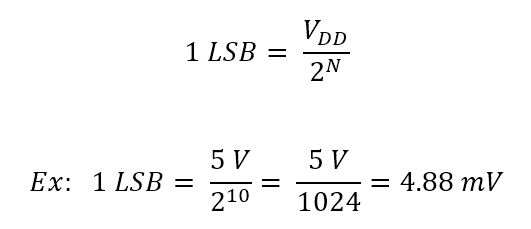
If we change the amplitude and the
offset to 2.44 mV
each, then the size of the LSB can be demonstrated in simulation, as
seen below:
This concludes the pre-lab work for Lab 2.
Lab objectives
-
Document
the design of a 10-bit DAC using an n-well R of 10K.
-
Show how to determine the output resistance of the DAC by
combining resistors in parallel and series.
-
Document the delay of the circuit while driving a load.
- Show how to create a symbol view for the DAC design with
the same footprint as the ideal DAC from the pre-lab.
Lab
The design of our 10-bit DAC will be
based on the schematic below, taken from the EE 421L lab page for Lab 2:
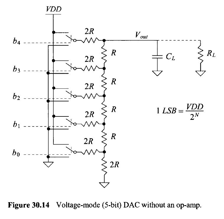
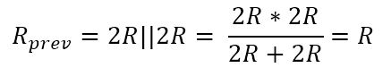
Determining
Resistance
Resistance in a 10-bit DAC can be
determined by evaluating the circuit looking in from the ADC outputs.
The equation below shows how the two 2R resistors in parallel will
create an R resistor in series with R, thus creating another 2R
resistor.
This then cascades throughout the
circuit until the end when a 2R by 2R voltage divider is formed.
Design Documentation
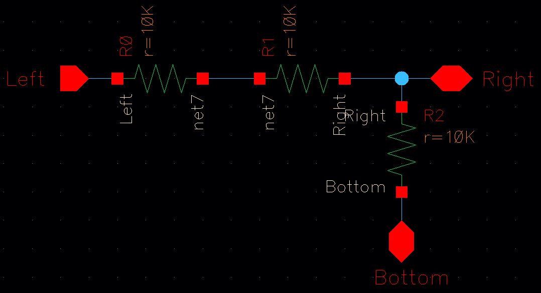
1. First we construct a single bit
voltage divider as seen in the 10-bit schematic, except without the
switches. We assume R = 10K. The schematic can be seen in the image
below.
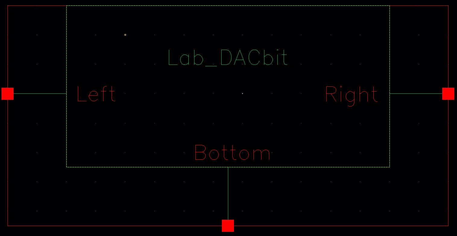
2. Now we will export this schematic by creating a symbol. To do this
we select Create->Cellview->From Cellview. Make sure that
your pins are set in the right order and to the right sides of the
sytmbol. Click OK.
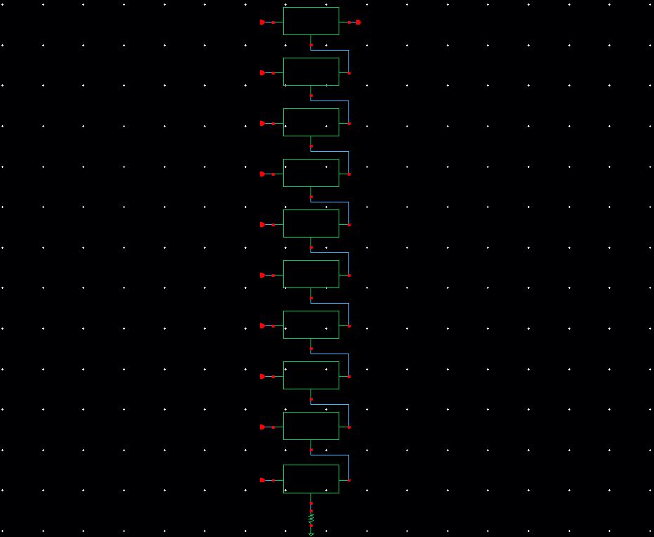
3. Next we will arrange 10 of these symbols from top-to-bottom, and
create the pins and connections for each according to the 10-bit DAC
schematic. It should look like the image below:
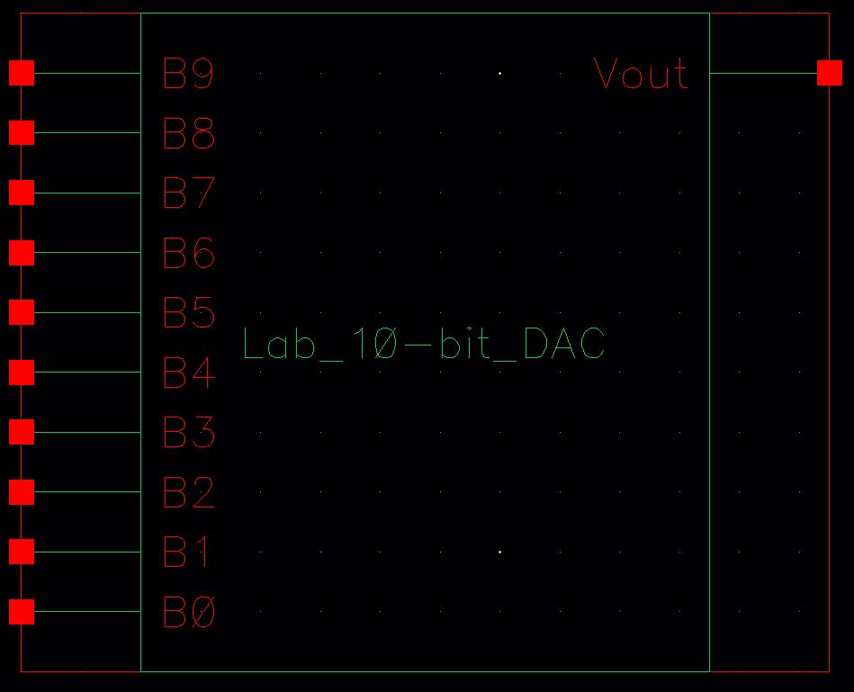
4. Again, we will export the schematic to a symbol as in Step 2. Make
sure that the bits are in the correct order (top->bottom). The
symbol should look like below:
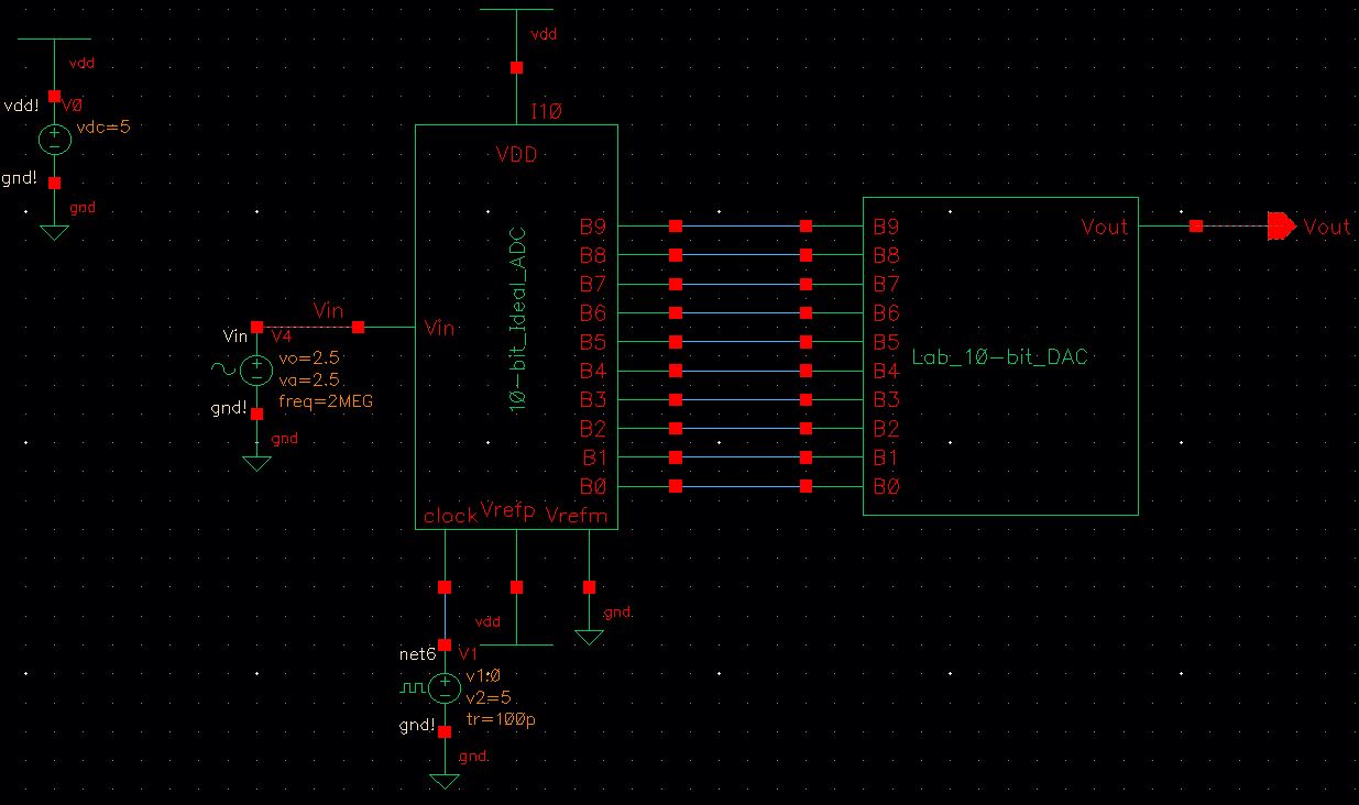
5. Finally, we will import this symbol into the schematic for our
10-bit ADC-DAC. The final schematic will look like the image below:
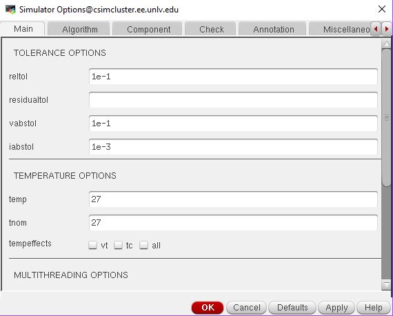
8. Edit the simulation options to be like the image below:
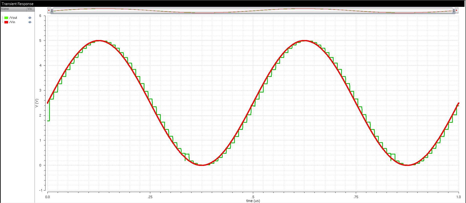
7. Simulate the output and compare to the original DAC implementation.
Output should look similar to the below image:
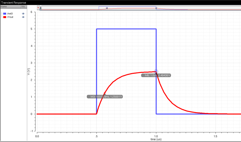
RC Delay
(driving a load)
The delay through the DAC can be
determined using the formula shown below. After plugging in the
resistor and capacitor values for the circuit, an RC delay of 70 ns is
obtained.

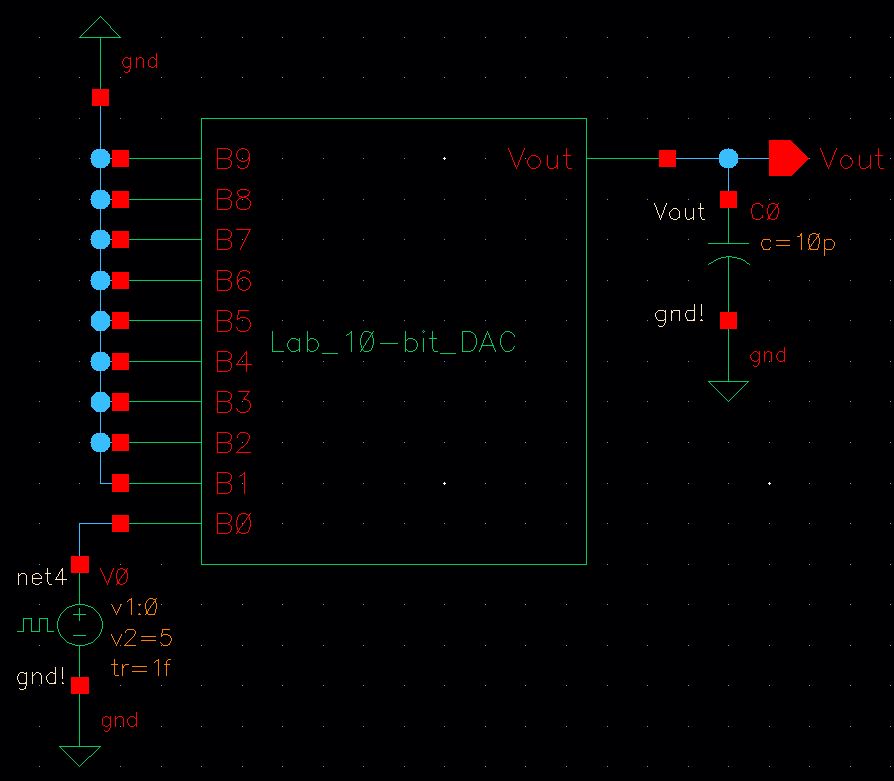
We can confirm this value by
simulating the circuit. Below is a schematic of the circuit. To acheive
this, we apply a 5V pulse to the first bit of the DAC, and then ground
the rest of the inputs.
The simulation of the RC delay
shows that the time constant for the RC delay of the 10-bit DAC is
approximately ~70 ns.
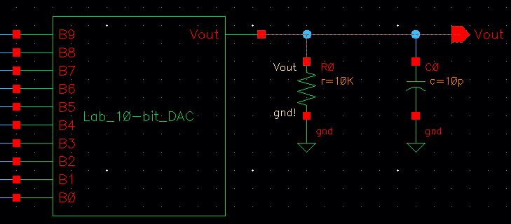
Resistive Load (10K)
The following is a schematic of the
10-bit ADC-DAC when simulated with a 10K resistive load on the output.
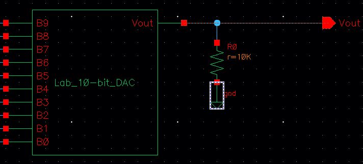
The simulation results show that the resistive load causes the output
to be reduced to half of the originial output:
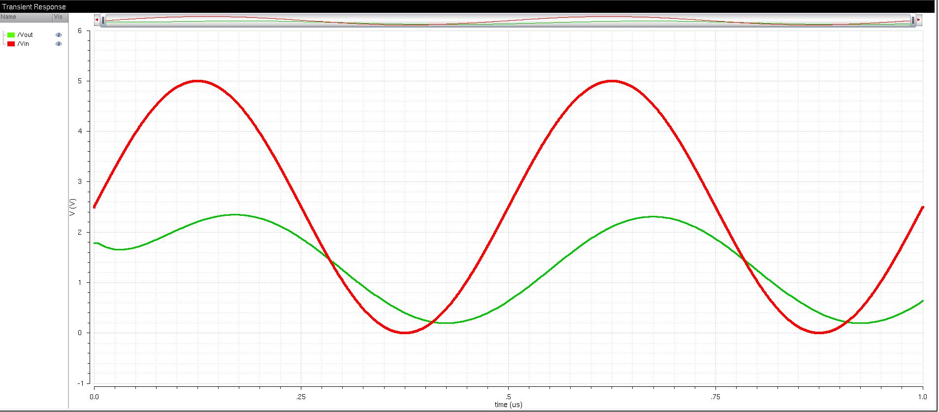
Capacitive Load (10
pF)
The following is a schematic of the
10-bit ADC-DAC when simulated with a 10 pF capacitive load on the
output.
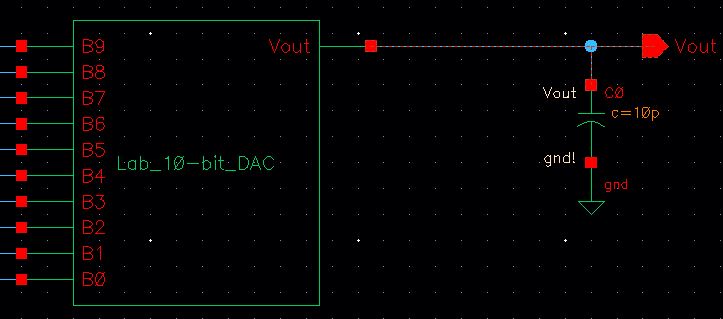
The
simulation results show that the capacitive load helps to smooth the
output of the DAC, due to the capacitor's charge. This also causes a
phase shift in the output.
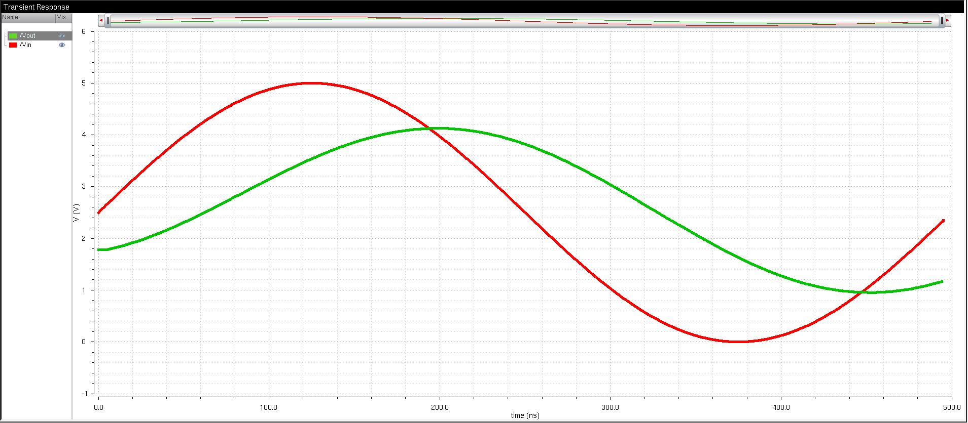
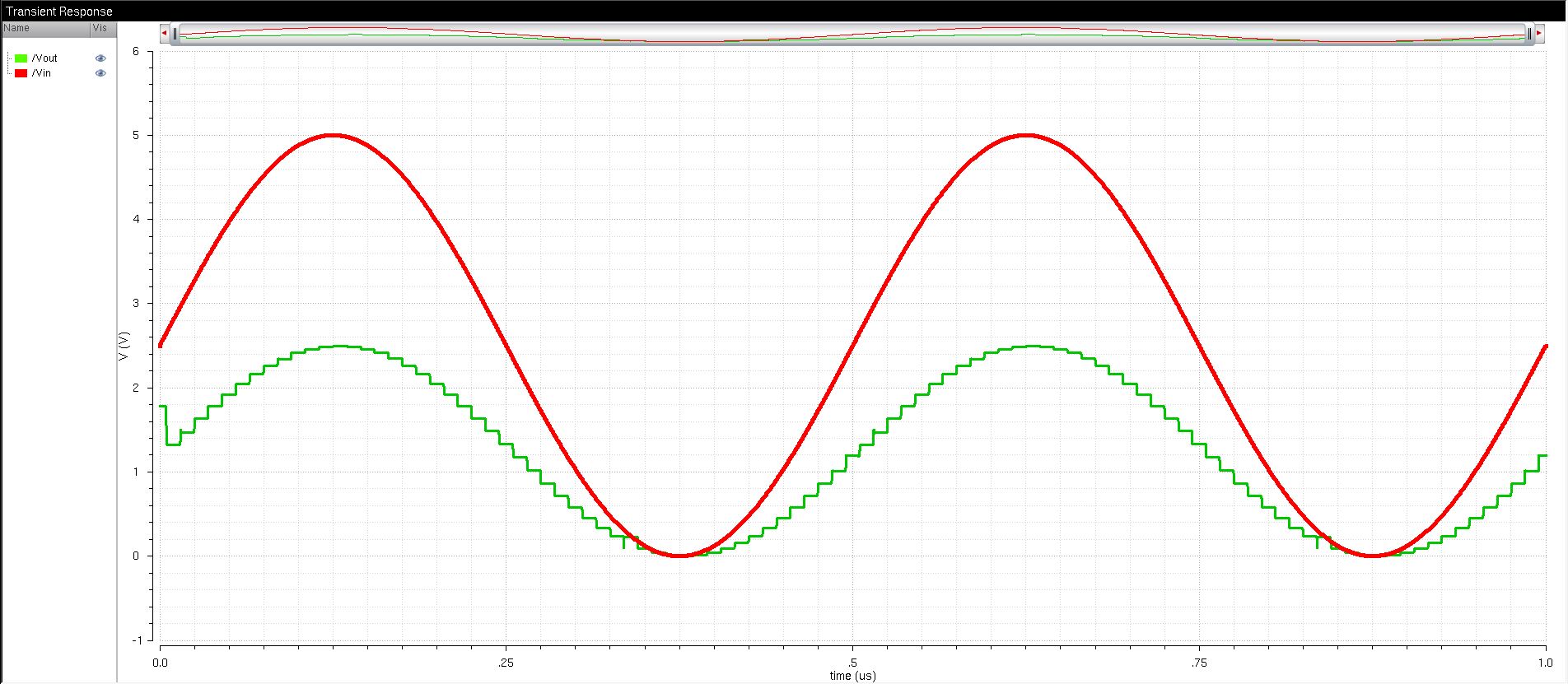
Resistive & Capacitive
Load
When both the resistive and capacitive loads are applied to the output,
the effects of both individual loads can be seen. Below is a schematic
of the final circuit:
The
simulation results show the effects of both the resistive and
capacitive loads being applied to the output. This includes a reduced
amplitude due to the resisitive load, and a smoothed and shifted
waveform due to the capacitive load.
This concludes the main content for Lab 2.
Return
to My Labs