Lab 8 - ECE 421L
Authored
by
Jovanne Dahan (dahanj1@unlv.nevda.edu)
Esteban Tuquero (tuqueroe@unlv.nevada.edu)
December 5, 2018
Description
Generating a test chip layout for submission to MOSIS for fabrication.
Chip includes the following devices
- One course project (Serial-to-Parallel Converter)
- A 31-stage ring oscillator with a buffer for driving a 20 pF off-chip load
- NAND and NOR gates using 6/0.6 NMOSs and PMOSs
- An inverter made with a 6/0.6 NMOS and a 12/0.6 PMOS
- Transistors,
both PMOS and NMOS, measuring 6u/0.6u where all 4 terminals of each
device are connected to bond pads (7 pads + common gnd pad)
- Note
that only one pad is needed for the common gnd pad. This pad is used to
ground the p-substrate and provide ground to each test circuit
- Using
the 25k resistor laid out below and a 10k resistor implement a voltage
divider (need only 1 more pad above the ones used for the 25k
resistor)
- A 25k resistor implemented using the n-well (connect between 2 pads but we also need a common gnd pad)
- XOR gate
- Another 25k resistor using the n-well
Chip Design library can be found here Chip5_f18.zip
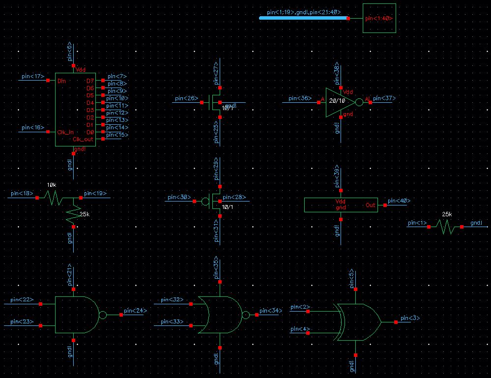
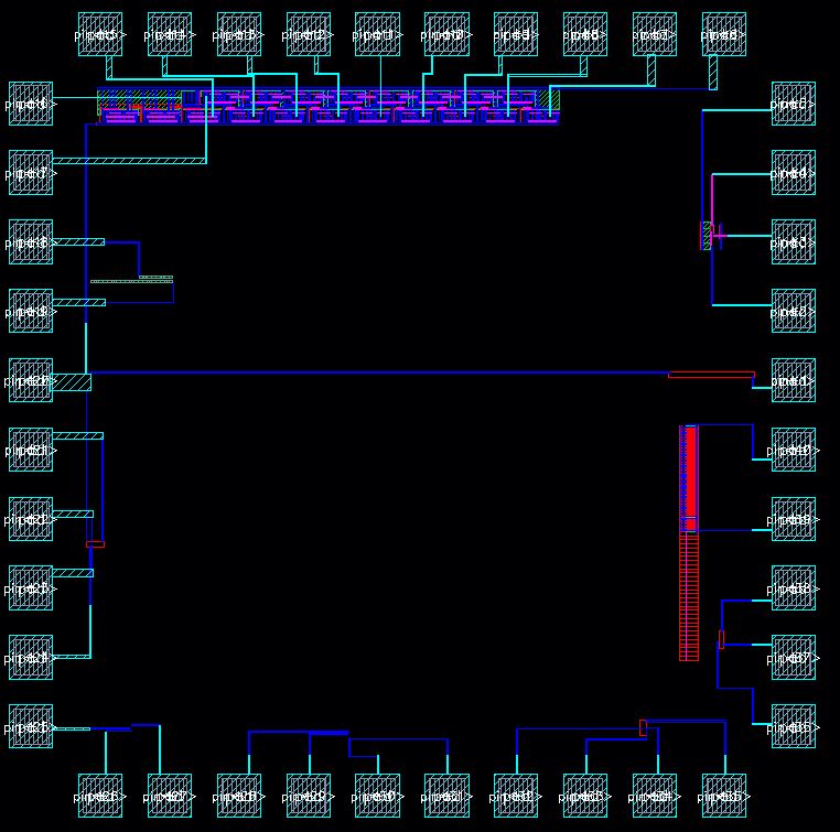
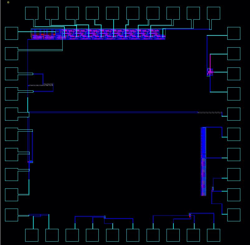
Chip
Pin Diagram


 |  |
| Schematic | Layout |
 |
| Extracted View |
 |  |
| DRC | LVS |
Device Testing
Serial-to-Parallel Converter
 | Pin # | Description |
| 6 | VDD of Converter |
| 7 | Parallel Output D7 |
| 8 | Parallel Output D6 |
| 9 | Parallel Output D5 |
| 10 | Parallel Output D4 |
| 11 | Parallel Output D3 |
| 12 | Parallel Output D2 |
| 13 | Parallel Output D1 |
| 14 | Parallel Output D0 |
| 15 | Clock Output (Clk_out) |
| 16 | Clock Input (Clk_in) |
| 17 | Input Data (Din) |
| 20 (gnd) | Ground |
The serial-to-parallel converter is the most complex circuit in the chip; however, it is quite simple to operate. The gnd of the schematic (as with all the others) is connected to pin<20> of the chip. Vdd should be connected to 5V because this was made with the C5 process. Clk_in will
be connected to a function generator and you may choose the frequency
of the clock. Din should also be connected to a function generator; the
values of Din at the positive edge of Clk_in will
be outputted to D7-D0 (where D7 is the most recent Din) every 8 cycles.
D7-D0 can be connected to LEDs to check if the output is changing every
8 cycles and more importantly to check if they are the right values.
Oscillator
 | Pin # | Description |
| 39 | VDD of Oscillator |
| 40 | Output of Oscillator |
| 20 (gnd) | Ground |
The oscillator only has 3 pins which makes it quite simple to operate. As always gnd connects to pin<20> and Vdd must be 5V. The output of the oscillator should be connected to an oscilloscope to check that the output is a square wave.
NAND Gate
 | Pin # | Description |
| 21 | VDD of NAND Gate |
| 22 | Input A |
| 23 | Input B |
| 24 | A NAND B |
| 20 (gnd) | Ground |
For the rest of the circuits, gnd is connected to pin<20> and Vdd must be connected to 5V. The operation of the NAND gate is simple: it will output a logic “0” only when A and B
are high (5V). Otherwise, the output will always be logic “1”. A and B
can be connected to DC sources, while the output should be connected to
an LED to check if it operates correctly for all possible input
combinations. Note: that if the LED lights up it means the output is a
logic “1”, and it is a logic “0” if it is off.
NOR Gate
 | Pin # | Description |
| 32 | Input A |
| 33 | Input B |
| 34 | A NOR B |
| 35 | VDD of NOR Gate |
| 20 (gnd) | Ground |
The operation of a NOR gate is as follows: if either A or B
is logic “1” then the output is a logic “0” – when A and B are logic
“0” then the output is a logic “1”. Similar to the NAND gate, this
would be easier to test with a DC source for the inputs while the
output is connected to a LED.
XOR Gate
 | Pin # | Description |
| 2 | Input A |
| 3 | A XOR B |
| 4 | Input B |
| 5 | VDD of XOR Gate |
| 20 (gnd) | Ground |
The operation of a XOR gate is as follows: if either A or B
is are different then the output will be logic "1" if A and B are the
same then the output will be logic "0". Similar to the NAND gate, this
would be easier to test with a DC source for the inputs while the
output is connected to a LED.
Inverter
 | Pin # | Description |
| 36 | Input Voltage |
| 37 | Inverted Voltage |
| 38 | VDD of Inverter |
| 20 (gnd) | Ground |
The
best way to test the inverter is to connect its input to a function
generator that is outputting a square wave. Use the oscilloscope to
compare the input and the output. The output should be the opposite of
the input: that is, when input is high output should be low (and vice
versa).
Voltage Divider
 | Pin # | Description |
| 18 | Input Voltage (Vin) |
| 19 | Output Voltage (Vout) |
| 20 (gnd) | Ground |
Here we have a voltage divider, which we know has the formula: Vout = Vin *R1/(R1+R0). For the voltage divider below Vout = Vin*0.286. Vin in this case can be connected to any DC value and Vout should be only 0.286 times that DC input. Vout should be connected to an oscilloscope or a multi-meter to check that the output is correct.
Resistor
 | Pin # | Description |
| 1 | Input Voltage |
| 20 (gnd) | Ground |
Here we have a simple 25kΩ resistor. To check its operation, a DC input should be connected to Vin,
and the current through the resistor should be measured with the
multi-meter. Using Ohm’s law you can determine if that current is
correct or not.
NMOS
 | Pin # | Description |
| 25 | NMOS Drain |
| 26 | NMOS Gate |
| 27 | NMOS Source |
| 20 (gnd) | NMOS Body (connected to Ground) |
A
NMOS also functions like a switch but it is better at passing logic
“0”. To test this, connect source and body to ground, with gate
connected to a square pulse. The drain should be connected to a
resistor and LED in parallel, with a DC (5V) source connected to the
resistor. With this setup, the LED should light up when gate pulse is
low and turn off when it is high.

PMOS
 | Pin # | Description |
| 28 | PMOS Body |
| 29 | PMOS Source |
| 30 | PMOS Gate |
| 31 | PMOS Drain |
A PMOS is good at passing Vdd,
so that is the test we will use for this component. PMOS and NMOS act
like a switch, where the gate controls whether it is open or closed.
For the PMOS, the switch closes when gate is logic “0” (gnd).
Connect the drain and body to 5V, while connecting the gate to a square
pulse. Connect a resistive load to the source so you can monitor the
source with an oscilloscope or an LED. As mentioned previously, when
the gate is high the switch is open and when it is low the switch is
closed. Therefore, Psource should only be high when gate is low.
Return to labs