Prelab
Go through Cadence tutorial 4
All files have been backed up on google drive

NAND Gate
Lab 6 - ECE 421L
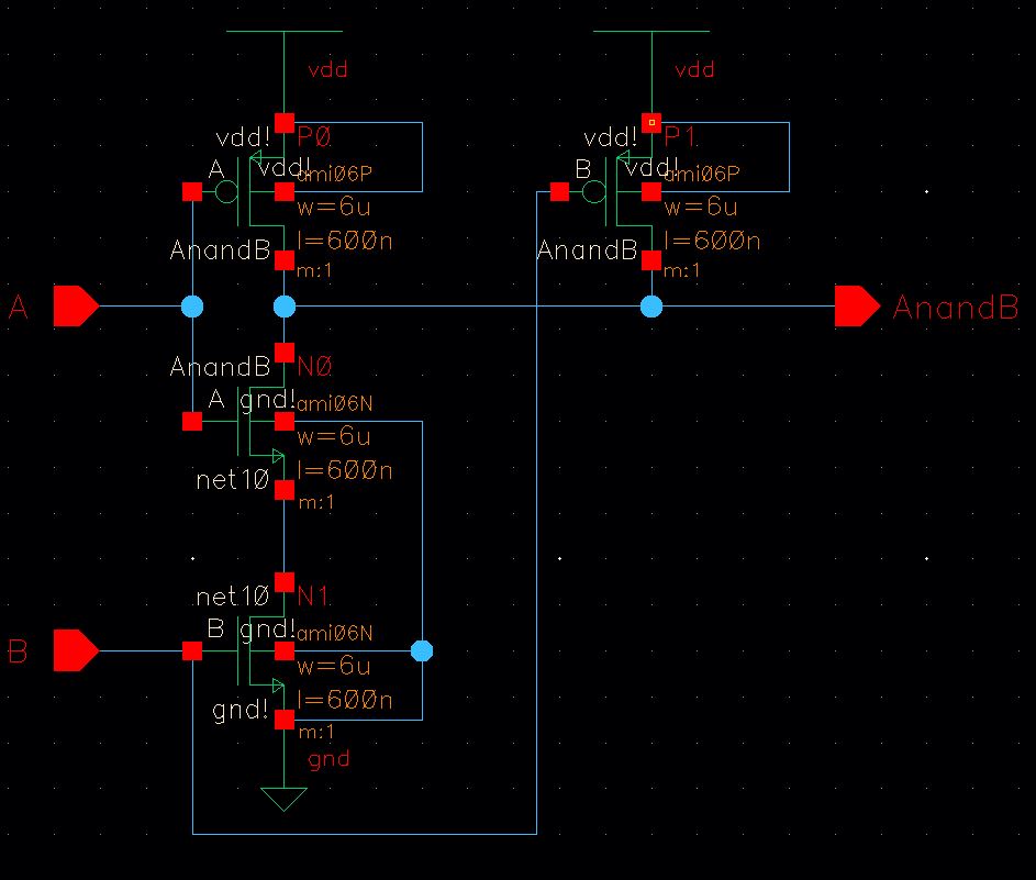 |  |
| Schematic | Symbol |
 |  |  |  |
| Layout | DRC | Extracted View | LVS |
 |  |
| Schematic | Symbol |
 |  |
| Layout | DRC |
 |  |
| Extracted View | LVS |
 |  |
| Gate Simulation Schematic | Simulation Results |
| Truth Table | ||||
| A | B | AnandB | AxorB | Ai |
| 0 | 0 | 1 | 0 | 1 |
| 0 | 1 | 1 | 1 | 1 |
| 1 | 0 | 1 | 1 | 0 |
| 1 | 1 | 0 | 0 | 0 |
 |  |
| Schematic | Symbol |
 |
| Layout |
 |
| DRC |
 |
| Extracted View |
 |
| LVS |
 |  |
| Full Adder Simulation Schematic | Full Adder Simulation Results |
| Full Adder Truth Table | |||||
| A | B | Cin | S | Cout | |
| 0 | 0 | 0 | 0 | 0 | |
| 0 | 0 | 1 | 1 | 0 | |
| 0 | 1 | 0 | 1 | 0 | |
| 0 | 1 | 1 | 0 | 1 | |
| 1 | 0 | 0 | 1 | 0 | |
| 1 | 0 | 1 | 0 | 1 | |
| 1 | 1 | 0 | 0 | 1 | |
| 1 | 1 | 1 | 1 | 1 | |