Course Project: Serial-to-Parallel Converter
Authored by James Skelly
Due Dates:
·
First half of the project (just the serial-parallel converter schematics, no layout), of your design and an html
report detailing
operation (including simulations), is due at the beginning of lab on Nov. 14.
·
Second
half of the project, a verified layout
and documentation (in html), is due at the beginning of lab on
Nov. 21.
Specifications:
·
Inputs: Din, clock_in
·
Outputs: D0-D7, clock_out
·
Speed of Operation:
o
Serial Input: 10Mbits/s
o
Parallel Output: 1.25MWords/s
·
Simulations: Show various inputs to prove the design works.
Zipped Up Lab Directory
<<Lab_Project.zip>>
----------------------------------------------------------------------------------------------------
Flip-Flop Design
The flip-flop schematic consists of four
transmission gates and four inverters.
Transmission Gate (TG) Using 6u/0.6u NMOS and PMOS
Devices


Inverter Using 6u/0.6u NMOS and PMOS Devices


D Flip-Flop Schematic (TGs and Inverters Use
6u/0.6u NMOS and PMOS Devices)

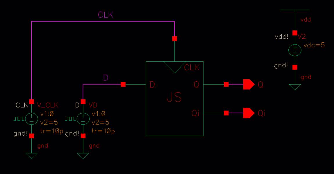
Symbol View of D Flip-Flop

The D Flip-Flop Contains inputs
D and CLK and outputs Q and Qi.
Layout and Extracted View of D Flip-Flop
LAYOUT

EXTRACTED WITH DRC AND LVS VERIFICATION


LVS and DRC verifications were successful, as can
be seen in the images above.
D Flip-Flop Simulation Results
The following
simulation tests the function of the D flip-flop. We can observe Q on different
rising clock edges.

From the
simulation above, we can observe that the D Flip-Flop is working properly.
·
For a Positive Edge-Triggered D Flip-Flop, Q gets D on the rising
edge of CLK.
·
The output Q floats until the clock signal rises, and Q gets D on
that edge.
·
The output Q goes low at 30us because D is low, and CLK pulses
high at 30us.
·
The output Q goes high at 70us because D is high, and CLK pulses
high at 70us.
·
The output Q stays high for the remainder of the analysis because
D is high on every clock edge.
The D
Flip-Flop that was created above will be the essential building block of the
three circuits that make up the serial-to-parallel converter.
These three
circuits are the shift register, hold
register, and clock divide circuits.
----------------------------------------------------------------------------------------------------
Shift Register
The 8-bit
shift register is created by cascading eight D flip-flops, the first of which
takes in a serial data input (in
this case, Din).
The output of
each flip-flop “Q” is connected directly to the data input of the next
flip-flop in the cascade.
The shift
register “shifts” data down the cascaded flip-flops on each rising edge of clock (in this case, clock_in).

The outputs of
each flip-flop are fed into an output
bus, Q<7:0>. This bus will be the input to the hold register.
Symbol View of Shift Register

Layout and Extracted View of Shift Register
ZOOMED IN LAYOUT VIEW

LAYOUT

EXTRACTED

DRC AND LVS VERIFICATION


We see that
the LVS and DRC verification were successful.
----------------------------------------------------------------------------------------------------
Hold Register
The hold
register is also created by instantiating eight D flip-flops, but not cascading
them as was done in the shift register.
The outputs
Q7-Q0 of the shift register are fed into the D inputs of the flip-flops in the
hold register.
The hold
register holds the data Q7-Q0 on the
D inputs until the clock signal (in this case, clock_out) has a rising edge.

Symbol View of Hold Register

We are trying
to output an 8-bit binary word in parallel, representing the serial input Din on the output bits D7-D0.
In order for all 8-bits to be output in parallel
at the same instant in time, we need a different clock signal, slower than clock_in, that
will pulse
after all 8 bits Q7-Q0 have been loaded onto the inputs of the hold register.
For this, we create the clock divide circuit.
Layout and Extracted View of Hold Register
ZOOMED IN LAYOUT VIEW

LAYOUT

EXTRACTED

DRC AND LVS VERIFICATION


We see that the LVS and DRC verifications were
successful.
----------------------------------------------------------------------------------------------------
Clock Divide
The clock divide
circuit takes in a “master clock” signal (clock_in) on the clock terminal
of the first flip flop.
Let Q be given
a random initial value 0. This means Qi has the value 1, which is fed into D.
When clock_in goes
high, Q gets the value of D, which is 1 here. After this first clock edge, Q is
now 1, and Qi is 0.
Qi and D share
the same value, so D is also 0. When clock_in pulses a
second time, Q gets the value of D, which is 0.
We now have clock_in which has gone through two clock
cycles, and Q is high for the first cycle, and low for the second.
This means Q
is effectively a clock signal with half the frequency of the master clock
signal.

Symbol View of Clock Divider

Layout and Extracted View of Clock Divider
ZOOMED IN LAYOUT VIEWS


LAYOUT

EXTRACTED


The clock divider has successful LVS and DRC
verifications as well.
Clock Divide Simulation Circuit

The simulation
below shows plots of the master clock signal (clock_in), along with the
outputs of the three D flip-flops
which make up
the clock divide circuit. Clock_in has a
frequency of 10MHz.

In the above simulation, T is the period of clock_in.
·
The output of the first flip-flop is clock_in divided by 2, or clock_over_2. (f = 5 MHz)
·
The output of the second flip-flop is clock_in divided by 4, or clock_over_4. (f = 2.5 MHz)
·
The output of the third flip-flop is clock_in divided by 8, or clock_over_8.
(f = 1.25 MHz)
o Clock_over_8 will be our clock_out signal which will be used to control
our hold register timing.
----------------------------------------------------------------------------------------------------
Creating Symbol View for Complete
Serial-to-Parallel Converter


Complete Serial-to-Parallel Converter Layout and
Extracted View
LAYOUT

EXTRACTED

DRC AND LVS VERIFICATION


Our LVS and DRC verifications for the overall
circuit are successful.
----------------------------------------------------------------------------------------------------
Simulation Results Using Piecewise Linear Voltage
Source
The image
below shows the top-level view of the converter, which will be used to run two
simulations
to test the
operation of the circuit.
Inputs to the
circuit include:
·
10 MHz clock signal, clock_in
·
Piecewise Linear Voltage Source, Din
Outputs of the
circuit include:
·
1.25 MHz (clock_in / 8) clock signal, clock_out
·
Parallel output bus of hold register, D<0:7>

----------------------------------------------------------------------------------------------------
Three distinct simulations were ran
to test the circuit’s operation.
·
In the first simulation, the piecewise linear voltage source
supplies 8-bit binary word 10011001
into the Din serial input terminal of the converter.
First Piecewise Linear Voltage Source Waveform for
Din


In the plot
above, we see the input signal Din
(starting at 10us) representing 8-bit serial input 10011001.
We see output
bits D7-D0 representing the 8-bit parallel output 10011001 after 1 full cycle
of clock_out
(goes high at 80 us).
----------------------------------------------------------------------------------------------------
Second Piecewise Linear Voltage Source Waveform
for Din
·
In the second simulation, the piecewise linear voltage source
supplies 8-bit binary word 01010111
into the Din serial input terminal of the converter.


In the plot
above, we see the input signal Din
(starting at 10us) representing 8-bit serial input 01010111.
We see output
bits D7-D0 representing the 8-bit parallel output 01010111 after 1 full cycle
of clock_out
(goes high at 80 us).
----------------------------------------------------------------------------------------------------
Third Piecewise Linear Voltage Source Waveform for
Din
·
In the third simulation, the piecewise linear voltage source
supplies 8-bit binary word 00001111
into the Din serial input terminal of the converter.


In the plot
above, we see the input signal Din
(starting at 10us) representing 8-bit serial input 00001111.
We see output bits
D7-D0 representing the 8-bit parallel output 00001111 after 1 full cycle of clock_out (goes
high at 80 us).
----------------------------------------------------------------------------------------------------