Lab 2 - EE 421L
Authored
by Marco Muñiz
Email : munizm1@unlv.nevada.edu
09/10/2018
Pre-Lab
PART 1
For
the Pre Lab portion, I will be explaining the step-by-step process of
uploading, addressing, opening, and simulating the Lab 2 folder, as
well as the files found withing.
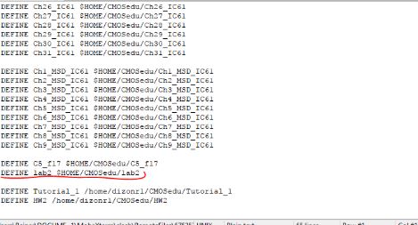
Step 1:
We
will download the Lab2.zip file onto our desktop and then onto the
CMOSedu folder in our csimcluster directory. Once this is done, we will
add the "DEFINE lab2 $HOME/CMOSedu/lab2" line onto the cds.lib file
found in our CMOSedu directory.
Step 2:
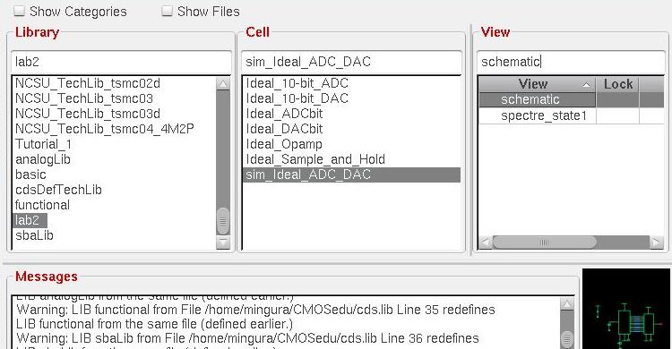
From
this point, we will navigate to the CMOSedu directory and open Cadence
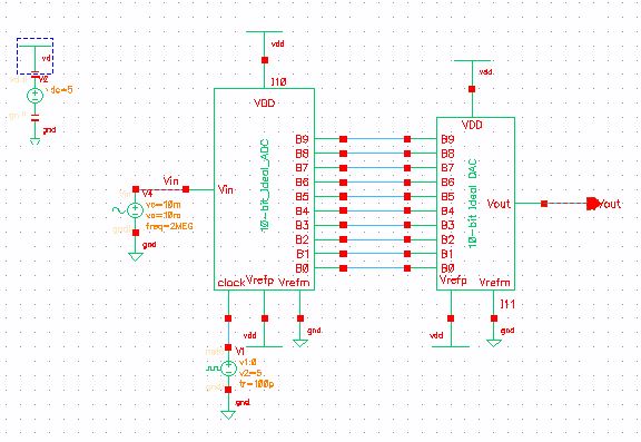
with the "virtuoso &" command. Then we will find the "Lab2" library
folder and open the Schematic for the "sim_Ideal_ADC_DAC".
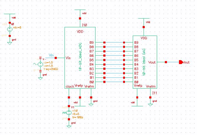
Step 3:
Lastly, we will open the schematic view for the ADC to DAC and simulate it with the loaded state.
PART 2
Step 1:
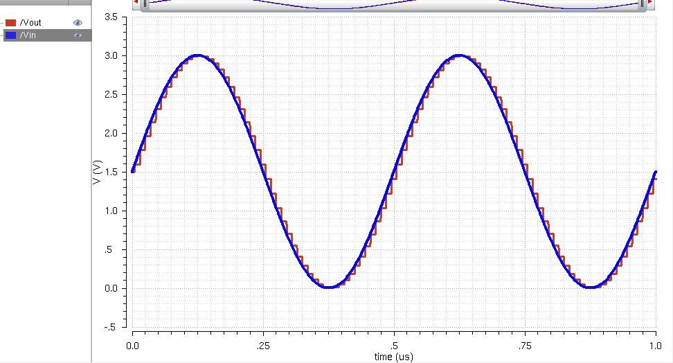
In
this part, we will be demonstrating our understanding of the above
simulation by making a slight change of the schematic and
re-simulating. I changed the input voltage to an amplitude of 10mV, as
well as the DC offset to 10mV. By doing so, we are able to see the
individual steps more clearly and can view the step size with a marker.
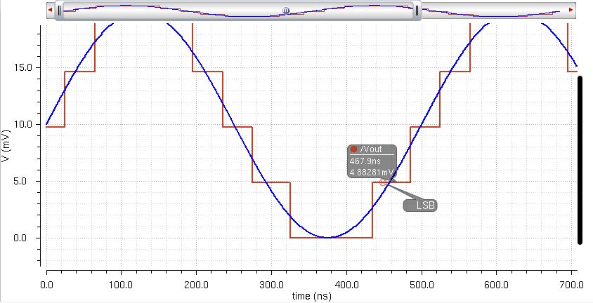
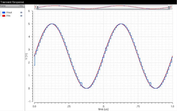
From
the above images, we can see that the step or LSB is roughly 4.883 mV
which is the amount that would be calculated by using the equation for
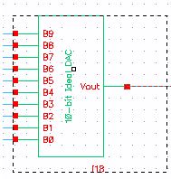
the LSB. Furthermore, we can deduce that B[9:0] represents the
input voltage "Vin" by way of 10 bits of data. When the input enters
the ADC, it is converted from an analog signal into a binary code with
each bit storing one digit. From this point, the binary code is inputed
into the DAC which converts it back to an analog signal but is
represented with steps instead of a continous waveform. However, by
increasing the number of bits, we can a more accurate representation of
the original waveform.
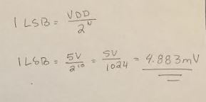
LSB = Least Significant Bit
N = Number of bits
___________________________________________________________________________________________________________________________________________________
LAB REPORT
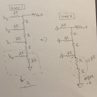
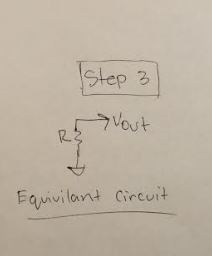
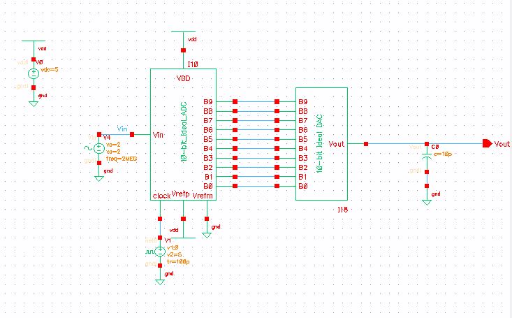
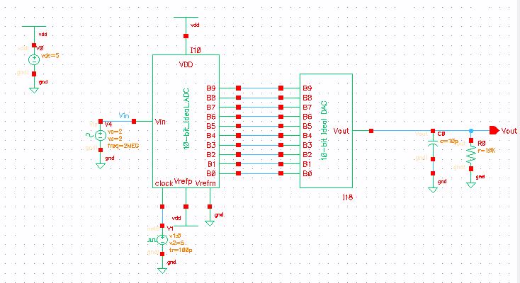
For the Lab, we will be designing a 10-bit DAC using an n_well R of 10k ohms.

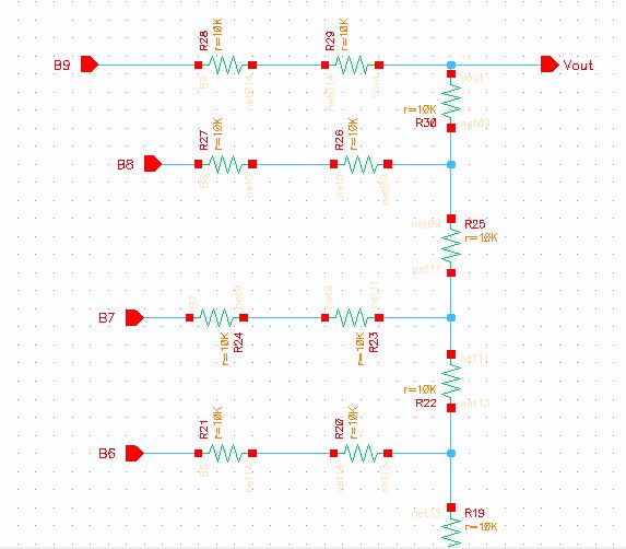
We must determin the output resistance of the DAC:
Since
the resistors are all of equivalent value and are in parallel, they
will continue to reduce to a final Equivalent Resistance of value "R".
This is illustrated in the bellow images.
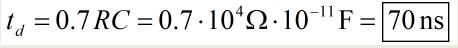
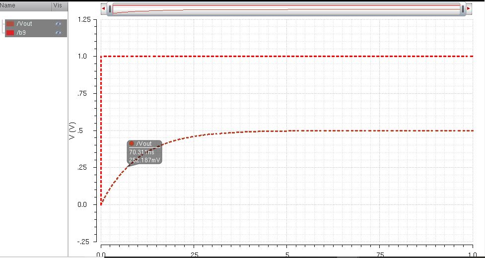
When
the DAC with all pins grounded, except for b9 which has a pulse added
to it, we would think that it would behave similarly to a RC circuit,
in which the delay can be calculated using 0.7RC. Below we can see the calculated delay value, as well as the simulation that support this calculation.
Creating a new symbol for your DAC design:
Copying over your designed DAC to the sim2_Ideal_ADC_DAC and Simulating:

From
the above simulations, we can see how they compare to the original
sim_Ideal_ADC_DAC circuit and see that they are the same in function.
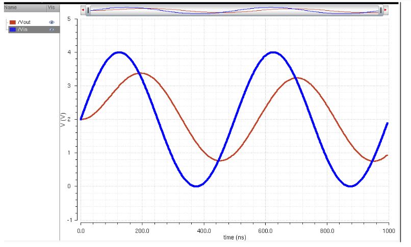
Same circuit as above but now driving a 10K Ohm load along with its simulation.

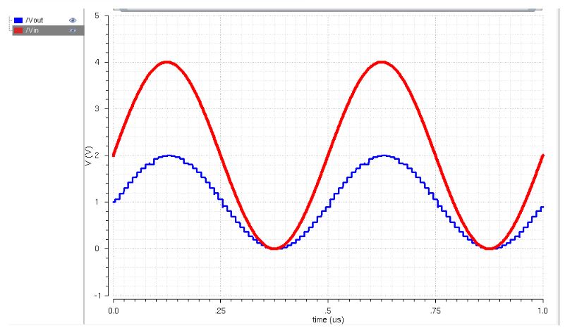
In the above simulation, we can see how adding the 10k Ohm resistor
created a voltage division which halved the input wave.
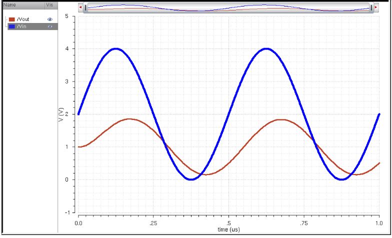
Same circuit as above but now driving a 10pF Capasitive load along with its simulation.
In the above simulation, we can clearly see the phase affect the capacitor has on the output.
Same circuit as above but now driving a 10K Ohm and 10pF load along with its simulation.
In
this last simulation, we can see that the 10k and 10pF load not only
halved the input wave due to the resistor but also shifted it because
of the capacitance.
What happens if the resistance of the switches isn't small compared to R:
Furthermore,
when we are applying series or parallel resistances to the DAC, the
output would voltage would be a lot lower than seen above.
Show proof of lab 2 back up.
My file is backed up on my Google Drive.
Return to My Lab's
Return to Student Directory
Return to CMOS Home