Lab 1 - ECE 421L
Authored
by Marco Muniz,
munizm1@unlv.nevada.edu
08/30/2018
Lab
description
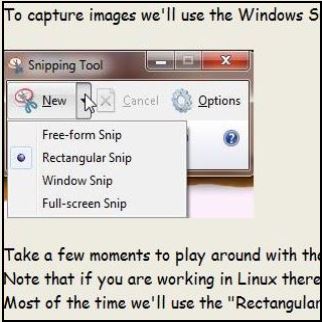
Image 1: The uploaded Snip.jpg image from the tutorial.
| 15648 | 89448 | Hi | Friend | 88855 | 12348 |
| 55263 | 84498 | 32155 | 56648 | 85214 | 963248 |
Lab 1:
In
this lab, we will be setting up our MobaXterm accounts, in order to be
able to use the Cadence design and simulation program. To do this, we
need to follow the steps within the set up to learn how to use the
functions of moba to create libraries and upload the needed files. Once
this was done, we used commands to navigate to the CMOSedu directory
and entered "Virtuoso &" into the command line to start the Cadence
program.

Image 2: Starting screen of cadence showing directory change and viruoso command.
Once
this is done, we created a library for lab one so that we could bring
up the folders and schematics that were unzipped in the last part. From
here, we needed to bring up the schematic for a voltage divider and
recreate it using a 1V supply and two 10K Ohm resistors. Once the
components were layed on the schematic palge, we connected them with
wires used the W hotkey and labeled these wires with the L hotkey.
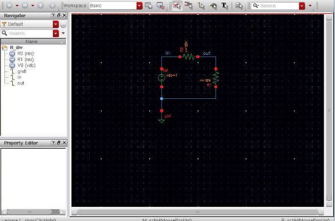
Image
3: Set up Voltage Divider Schematic with all labels. Once this has all
been set up, we can open the ADE L window in order to load the cell
view and run various types of simulations. In this case, we are
simulating the input and output voltage to show that the voltage
division is taking place.
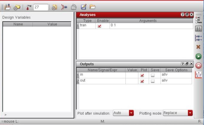
Image 4: The ADE window which shows the type of analysis being run, as well as what we are measuring.
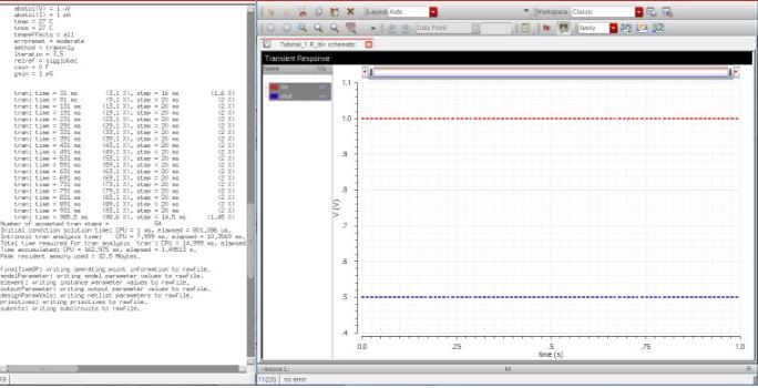
Image
5: In this transient analysis, we can see that the input voltage is
being measure at 1V and the output voltage is being measured at 0.5V.
This analysis shows that the voltage divider schematic is doing as
intended.
_____________________________________________________________________________________________________________________________________________
Part 2:
Backing up lab work
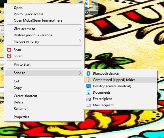
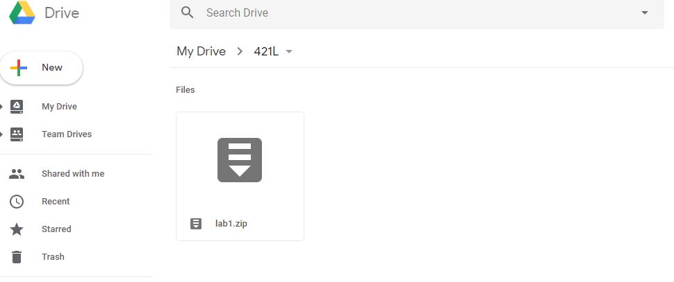
I
have decided to back up my lab files in zipped folders on google drive
and will frequenty re-save as I work on labs. I am doing this in case I
ever have in issue in future labs and can always reference back to a
past save to save myself from needless suffering. The steps to do this
can be seen in the images above.
Return to EE 421L Labs