Project - EE 421L Serial-to-parallel converter
Francisco Mata Carlos,
Email: matacarl@unlv.nevada.edu11/14/18
Lab
description:
The
goal of this project is to draft and layout a serial-to-parallel
converter. The converter takes the serial input data and outputs an
8-bit word and clock.
First half Project instruction:
- inputs to the circuit are Din and clock_in
- outputs to the circuit are D0-D7 and clock_out
- If the serial input is 10 Mbits/s then the parallel output is 1.25 MWords/s
- serial-parallel design should show various inputs to verify it works
First
a TG (Transmission Gate) and
symbol was created, then an edge-triggered D-FF was designed. 8 D-FF's
were connected in series making a shift register, which allowed to
store 8 serial bits. The outputs of each D-FF was connected to the
input of a second set of 8 D-FF's in parallel. The second set of 8
D-FF's is being
control by a second clock 8 times slower than the clock controlling the
first set of 8 D-FF's, generating an a 8-bit parallel output
when clock_out goes high. The clock used on the first set of 8
D-FF's was
set to a period of 100ns, because the input data is being represented
as 10Mbits per second. The clock that is controlling the second set of
D-FF's is the same clock divided by 8 (clock_out), which means that the
frequency will decrease 8 times, or for this case one periodis equal to
800ns
. The second clock or clock_out was created by taking the first clock
or input clock
and use it on 3 cascaded D-FF's. By doing this the Q output of the
third D-FF decreases the frequency of the input clock by 8 times.
Below is the TG (Transmission gate) schematic and symbol
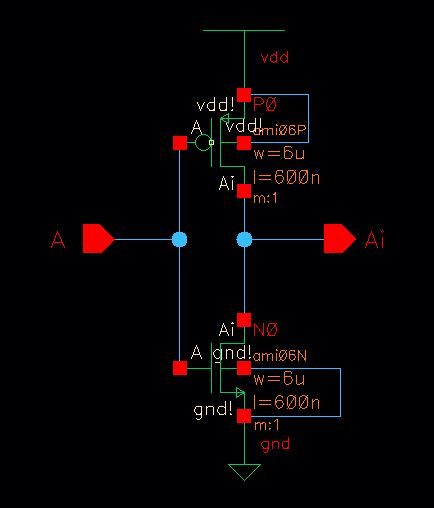
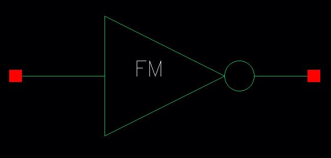
Below is the inverter schematic and symbol
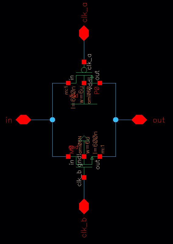
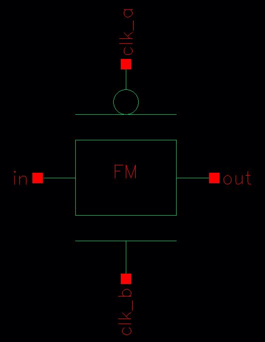
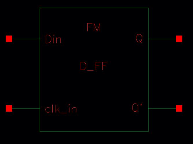
Below are the schematic and symbol for the edge-triggered D-FF 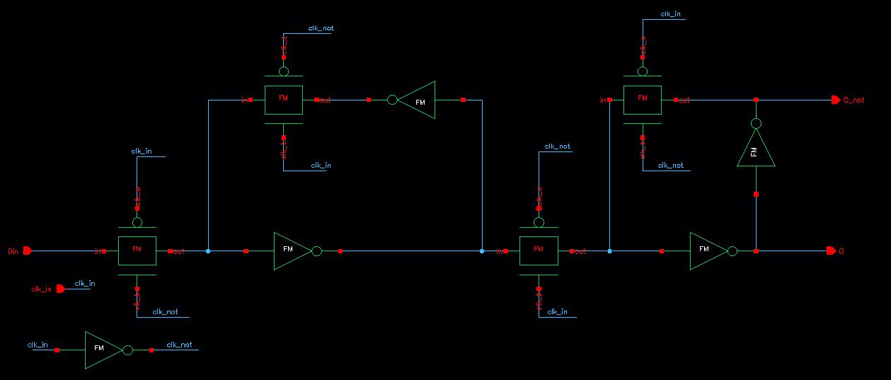
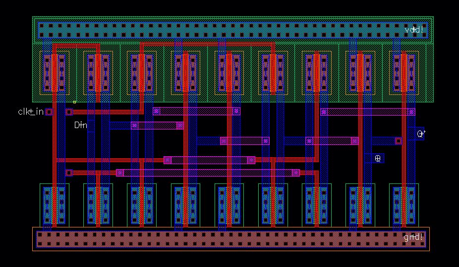
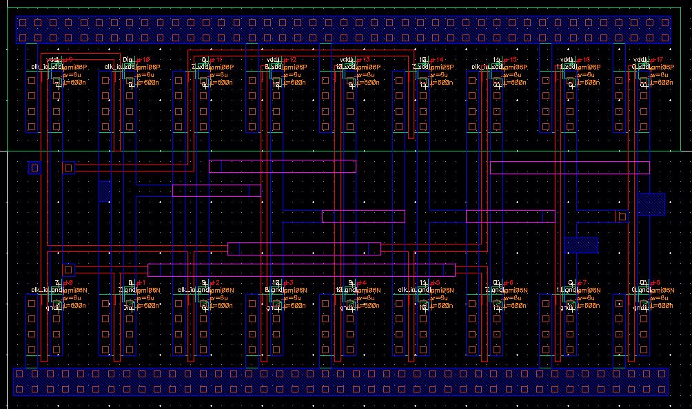
Below are the D-FF Layout and extracted view
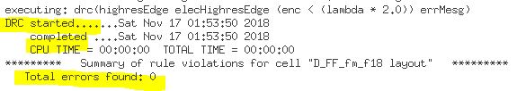
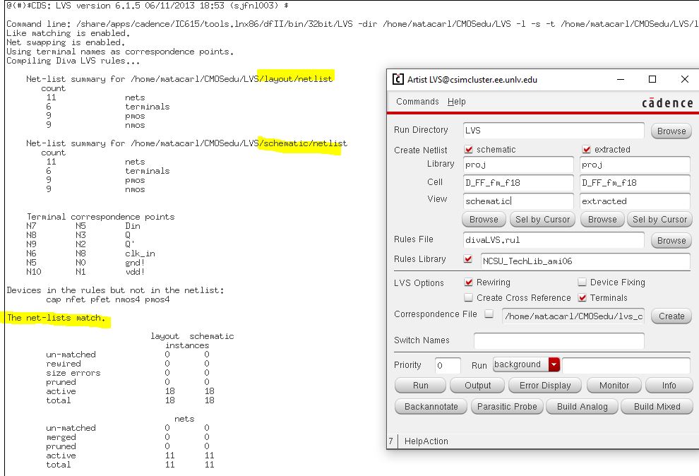
Below are the DRC and LVS for the DFF
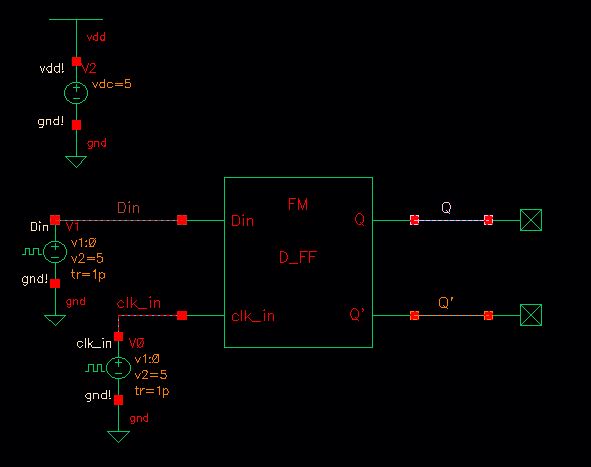
Below are the simulation schematic and plot for the D-FF
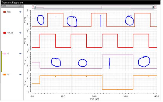
The plot above shows the edge-triggered
D-FF working correctly. When the clock goes high, Q outputs the Din
(input) bit that is at that instant, and the output maintains that same
bit until the next clock cycle.
Below are the simulation schematic and plot for the first set of 8-D-FF's or shift register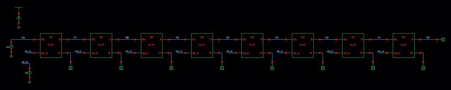
The simualtion below shows that the bits are shifted from left to right at each clock cycle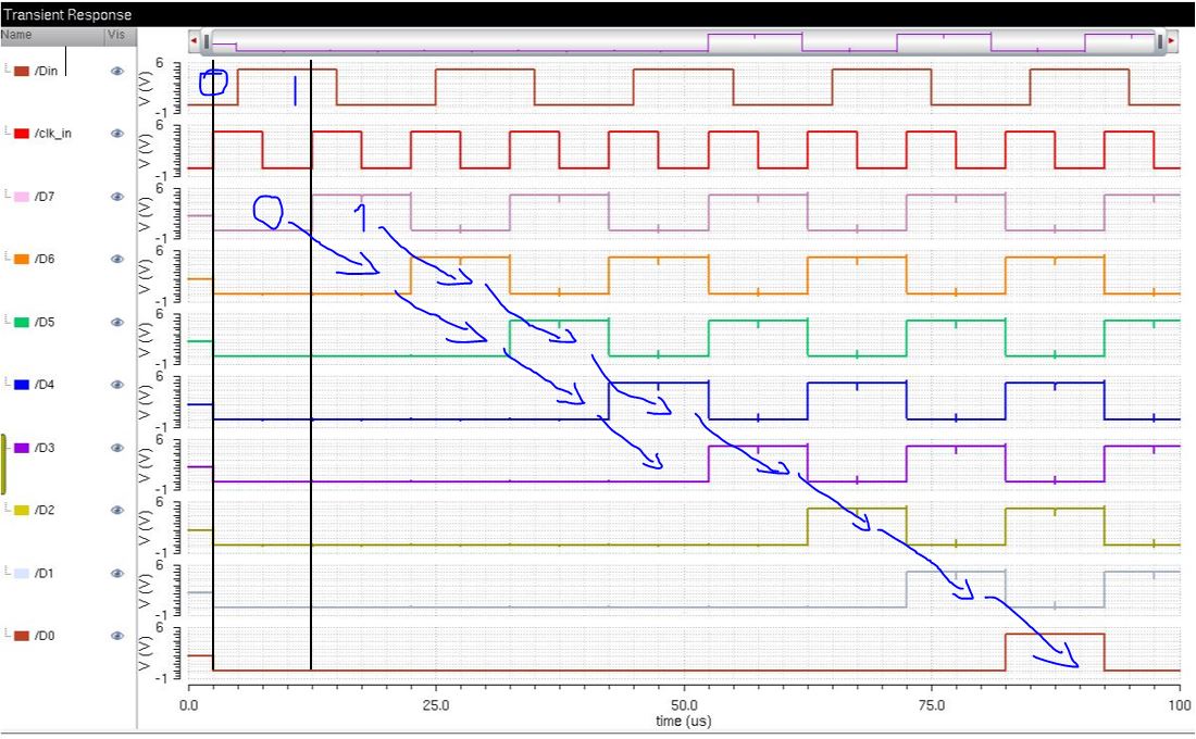
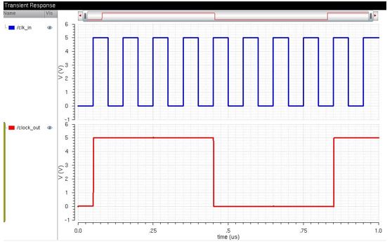
Below
are the schematic and plot showing how clock_out was created. Clock_out
is basically the input clock divided by 8, or decreased by 8 times. 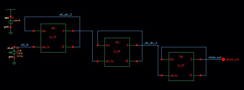
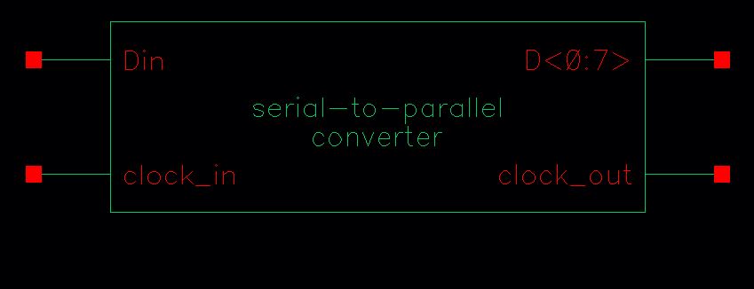
Below are the schematic and symbol for the Serial-to-Parallel converter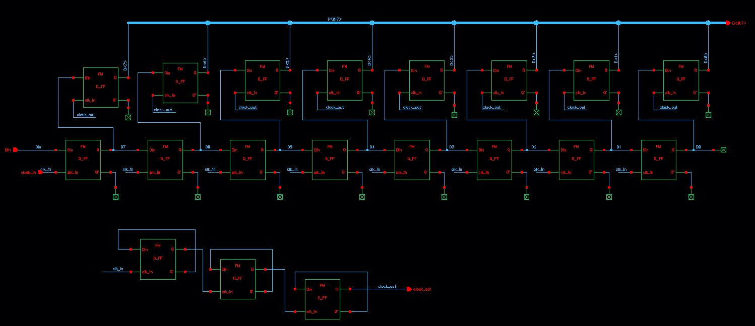
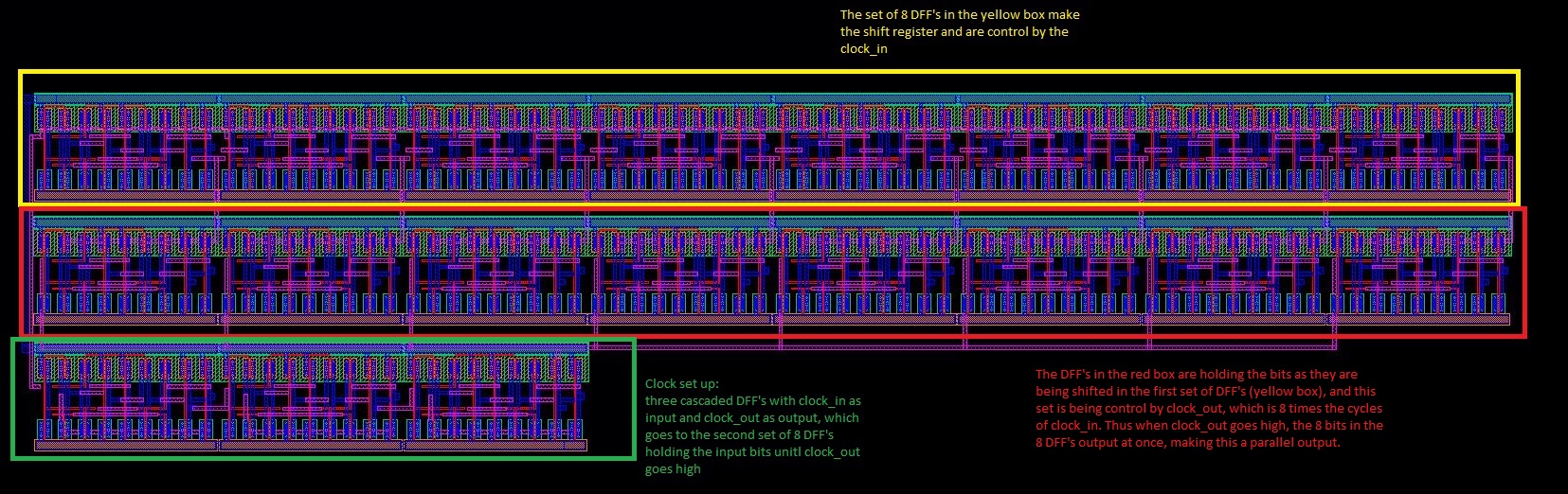
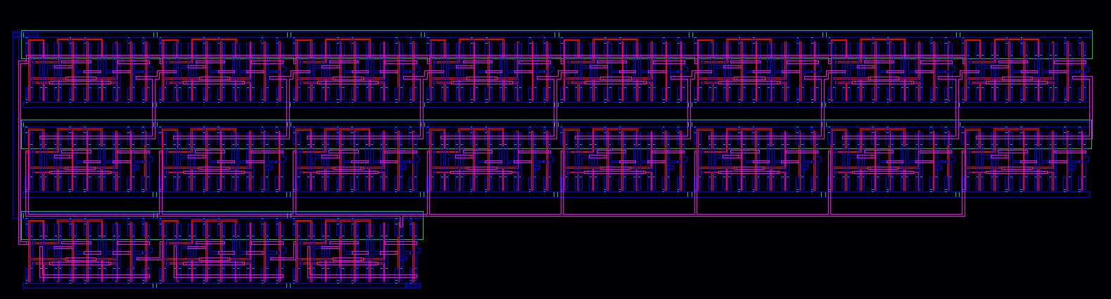
Below are the layout and extracted view for the serial-to-parallel converter
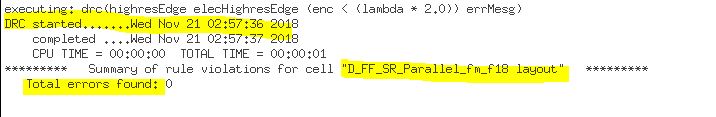
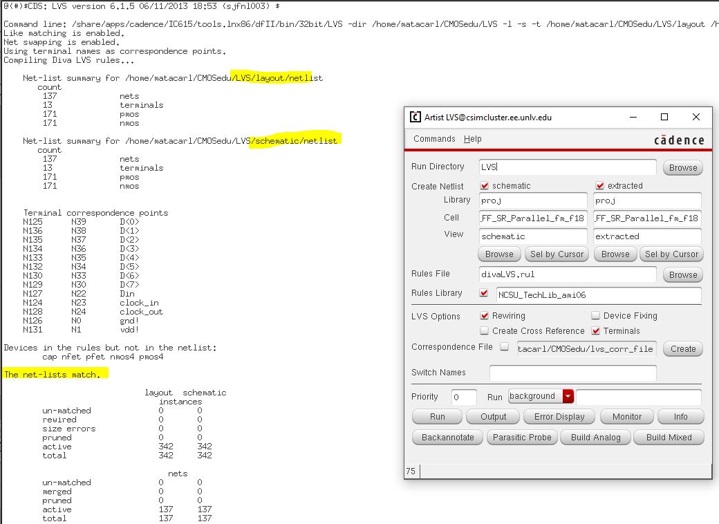
Below are the DRC and LVS for the serial-to-parallel converter
Below
are the simulations schematic along with different plots, showing the
Serial-to-Parallel converter generate a parallel 8-bit output from the
data input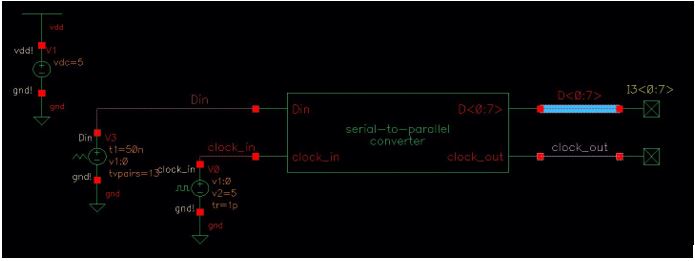
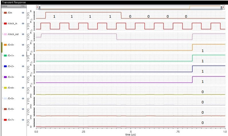
The serial data input used for this simulation is 00001111
(LSB is 1 and MSB is 0), however on the plot for the input data (Din),
the data was reversed because the inputs are shifted through from D7
through D0 (D7 being the first D-FF on the left and D0 being the last
on the right). The ouput D<7:0> shows the correct 8-bit word as
intended; D<0:3> having an output high and D<4:7> haing and
an outpul low.
The serial data input used for this simulation is 11010011
(LSB is on the right), however on the plot for the input data (Din),
the data was reversed because the inputs are shifted through from D7
through D0 (D7 being the first D-FF on the left and D0 being the last
on the right). The ouput D<7:0> shows the correct 8-bit word as
intended; D<0:1>=5V, D<2:3>=0V, D<4>=5V, D<5>=0V, D<6:7>=5V. 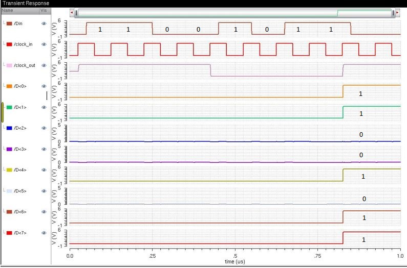
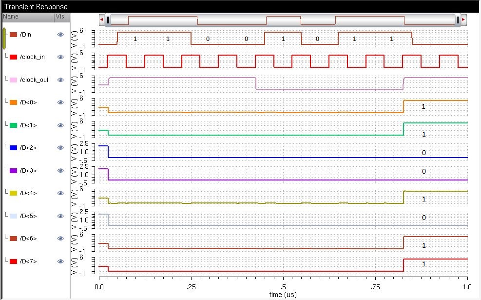
The serial data input used for this simulation is 11110000
(LSB is 0 and MSB is 1), however, again on the plot for the input data (Din),
the data was reversed because the inputs are shifted through from D7
through D0 (D7 being the first D-FF on the left and D0 being the last
on the right). The ouput D<7:0> shows the correct 8-bit word as
intended; D<0:3> having an output low and D<4:7> haing and
an outpul high.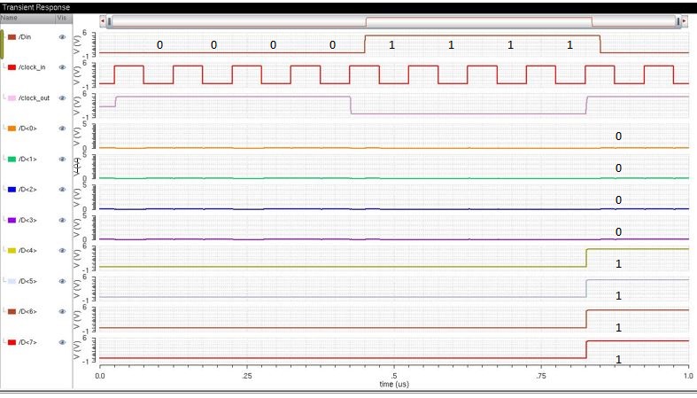
Below is the simulation for the serial-to-parallel converter using the extracted view to show the layout works 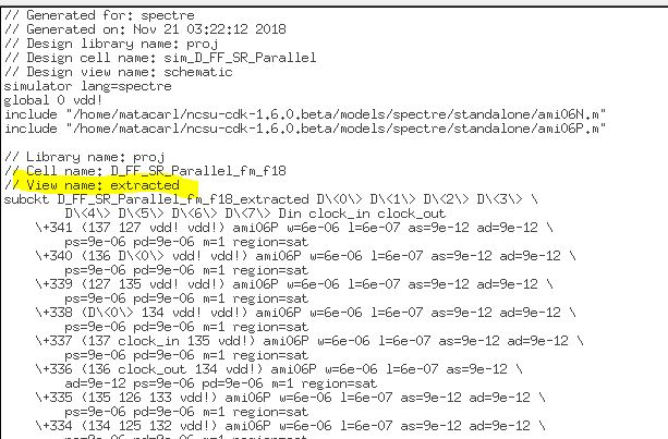
The schematic, and simulation files can be found here proj_fmc
Return to student lab reports
Return to labs