Lab 2 - EE 421L
Pre-lab:
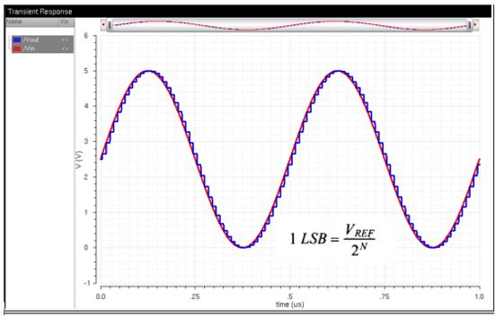
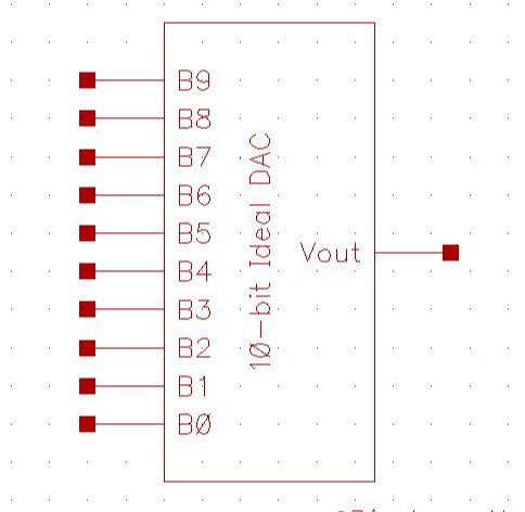
Downloaded lab2.zip to the desktop and upload to the design directory. This file contains an ideal 10-bit Analog-to-Digital Converter (ADC) and Digital-to-Analog Converter (DAC). The cell with the 10-bit ADC and DAC sim schematic was open and simulated to understand the relationship between the input voltage, the Bit inputs, and Vout.
The input was replaced with a small input voltage of 15mV to
see the output voltage step changes (each step is 1LSB) at the vout node, which
increases with each possible Data input.
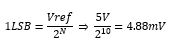
The picture below shows the step voltage to be about 4.88mV as was specified with the equation above.
Lab
description:
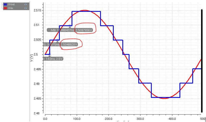
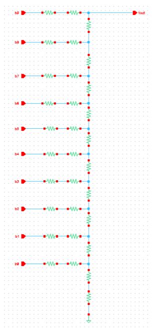
Create a 10-bit DAC using the topology (R-2R) in Fig. 30.14
shown below, create a symbol and simulate it using different loads
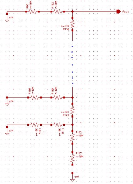
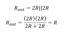
Determining the output resistance
By replacing the inputs on the left with ground and applying the formula below, the total output resistance is R or 10kΩ
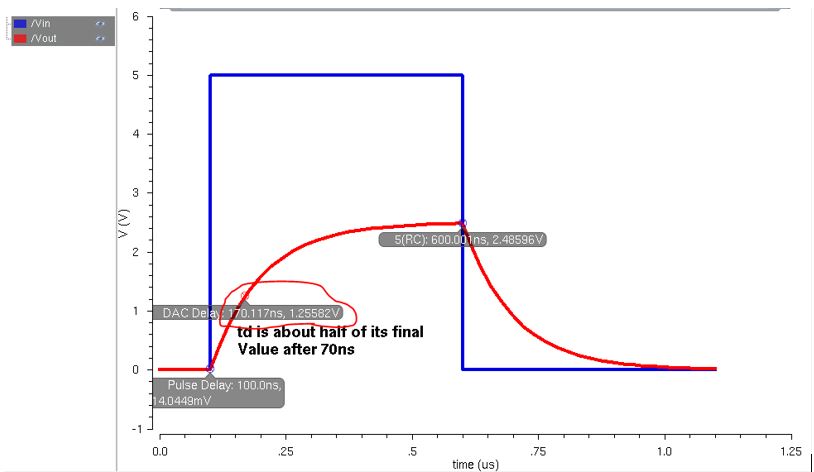
Delay when driving a 10pF load
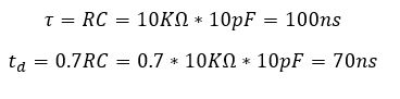
Below is a simulation using a pulse from 0 to 5V with a delay of
100ns. After 5RC (500ns) the output is about half the input which shows this
behaves as a voltage divider. Time delay (td) is about 1.25V at about 70ns,
which is what was expected.
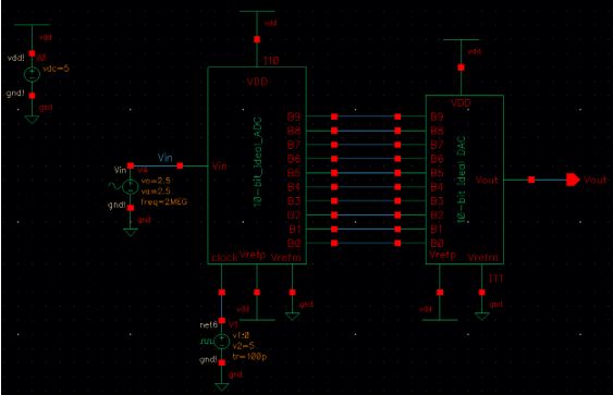
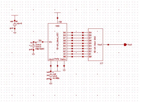
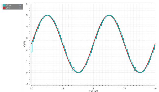
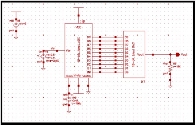
Schematic below shows the ADC connected to a DAC of my own design using R-2R topology, with no load. And the Simulation result below shows the output of the new DAC in relation to the input, without no load
Below are the schematic and simulation of an Ideal ADC to DAC, driving a 10k load. The Simulation result for a 10k load, shows the output signal half of the input signal because the 10k load makes a voltage divider with the 10k output resistance, thus making the output half the input.
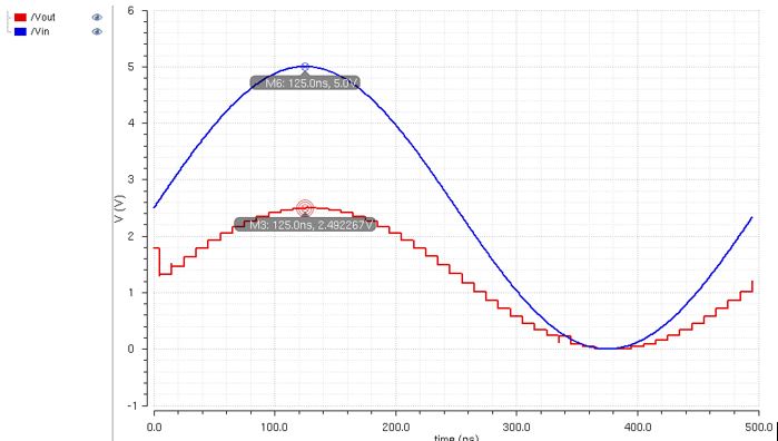
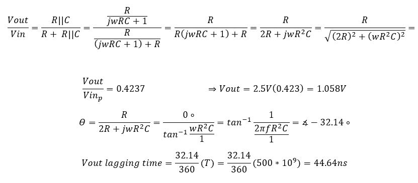
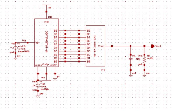
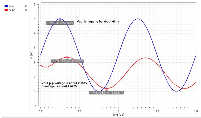
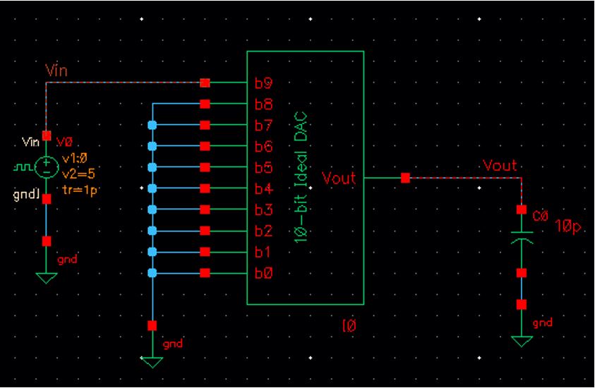
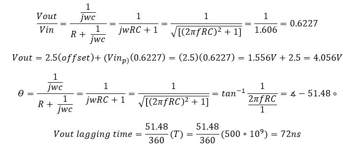
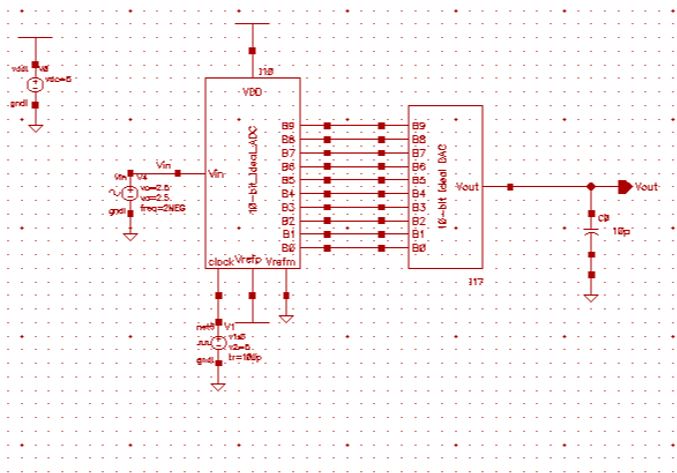
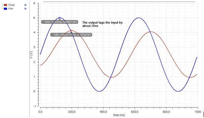
Below are the output equations, schematic, and simulation of an Ideal ADC to DAC, driving a 10pF load. The Simulation result for a 10pF load, shows the output signal lagging the input
Below are the output equations, schematic, and simulation of an Ideal ADC to DAC, driving a 10k and 10pF load. The simulation shows a decrease in voltage and a change in phase.