Project: Serial to Parallel Converter- EE 421L
Authored
by Victor Martinez
November 14, 2018
Design
a serial-to-parallel converter that takes serial input data and an
associated clock signal and generates an 8-bit output (parallel) word
and clock.
- The inputs to your circuit are Din and clock_in.
- The outputs to your circuit are D0-D7 and clock_out.
- If the serial input is 10 Mbits/s then the parallel output is 1.25 MWords/s.
First
half of the project (just the serial-parallel converter schematics, no
layout), of your design and an html report detailing operation (including simulations)
| Inverter Schematic | Inverter Symbol |
 |  |
| Transmission Gate Schematic | Transmission Gate Symbol |
 |  |
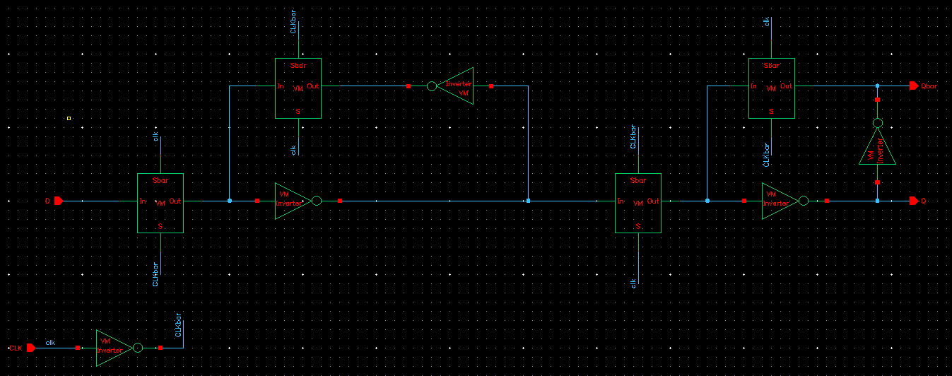
| D-Flip Flop Schematic | D-Flip Flop Symbol |
 |  |
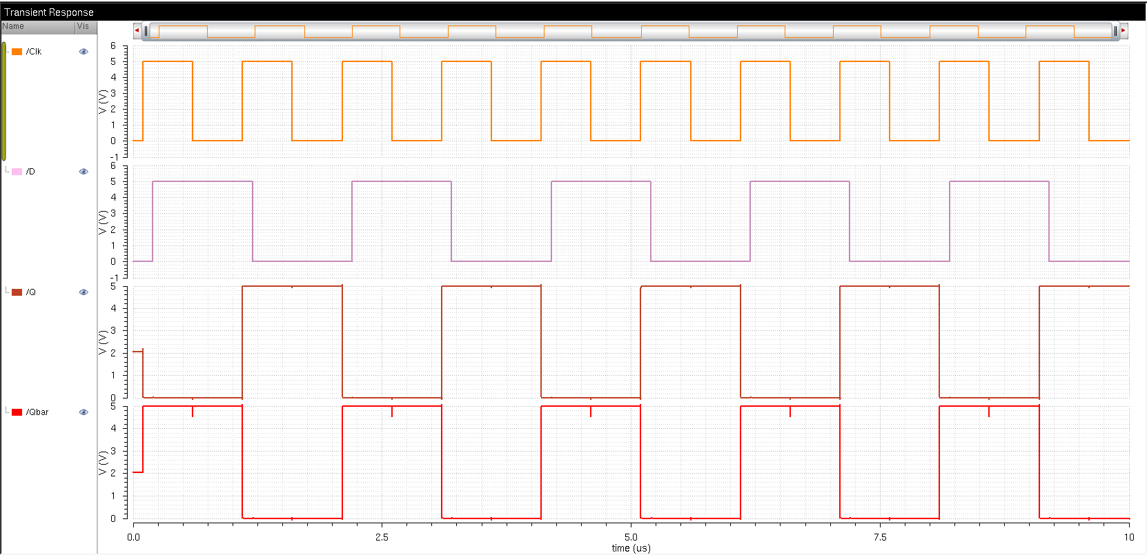
| DFF Simulation Schematic | DFF Simulation Plots |
 |  |
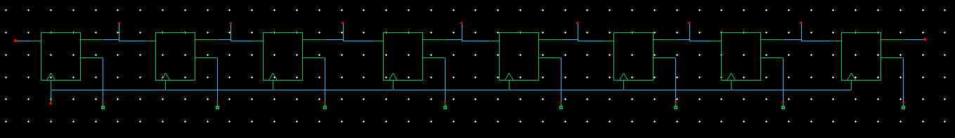
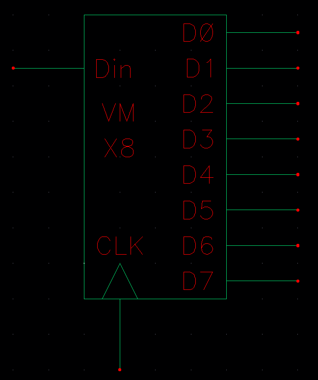
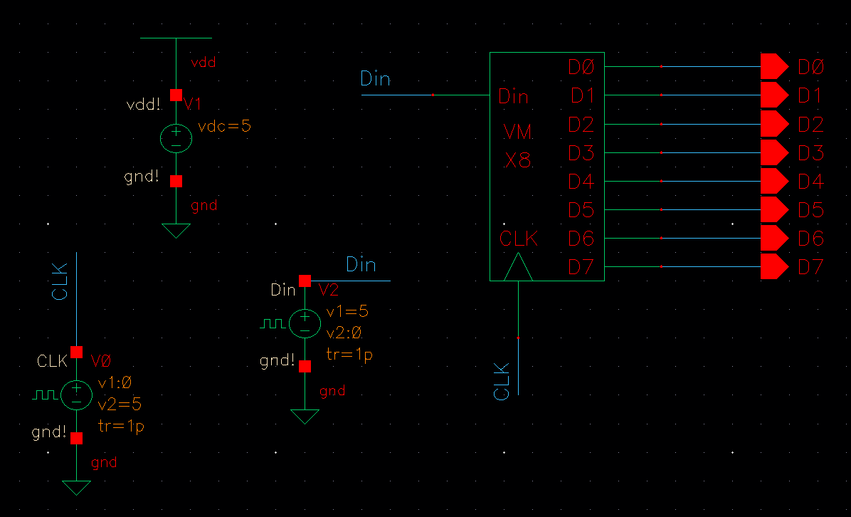
| 8-bit DFF Schematic (without CLK/8) | 8-bit DFF Symbol |
 |  |
| 8-bit DFF Simulation Schematic | 8-bit DFF Simulation Plot |
 |  |
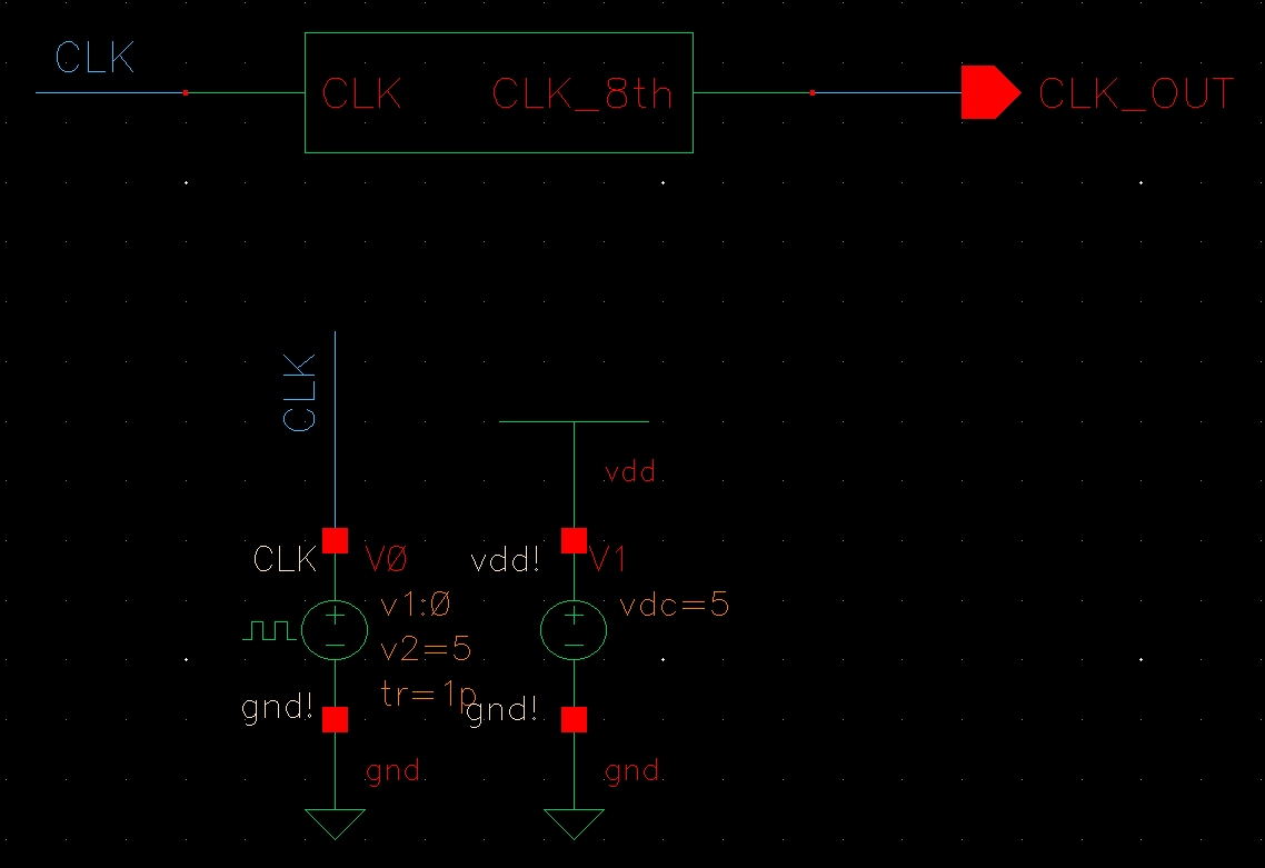
| CLK/8 Schematic | CLK/8 Symbol |
 |  |
| CLK/8 Simulation Schematic | CLK/8 Simulation Plot |
 | 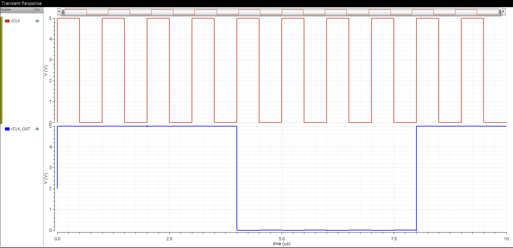 |
| 8-bit DFF Schematic (with CLK/8) | 8-bit DFF Symbol |
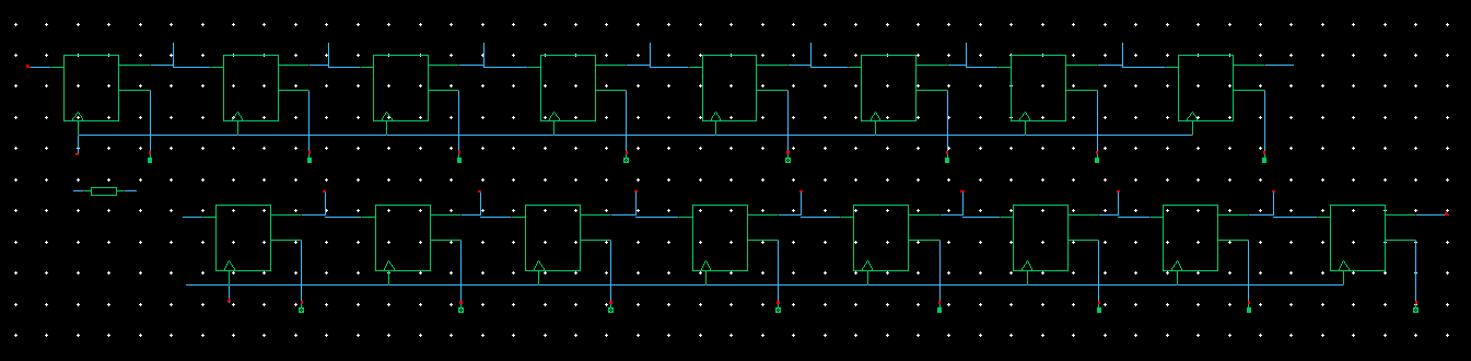 | 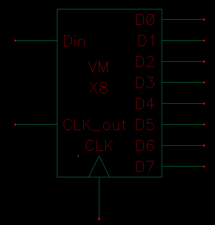 |
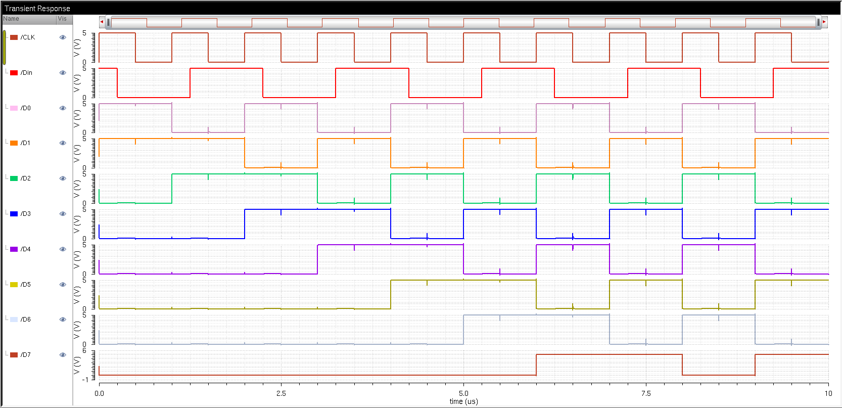
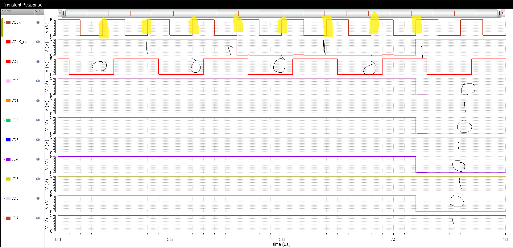
| 8-bit DFF Simulation Schematic (with CLK/8) | 8-bit DFF Simulation Plots |
 |  |
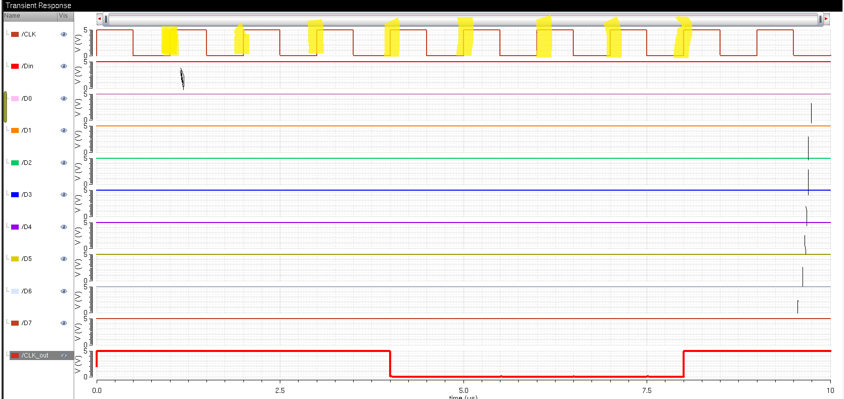 | 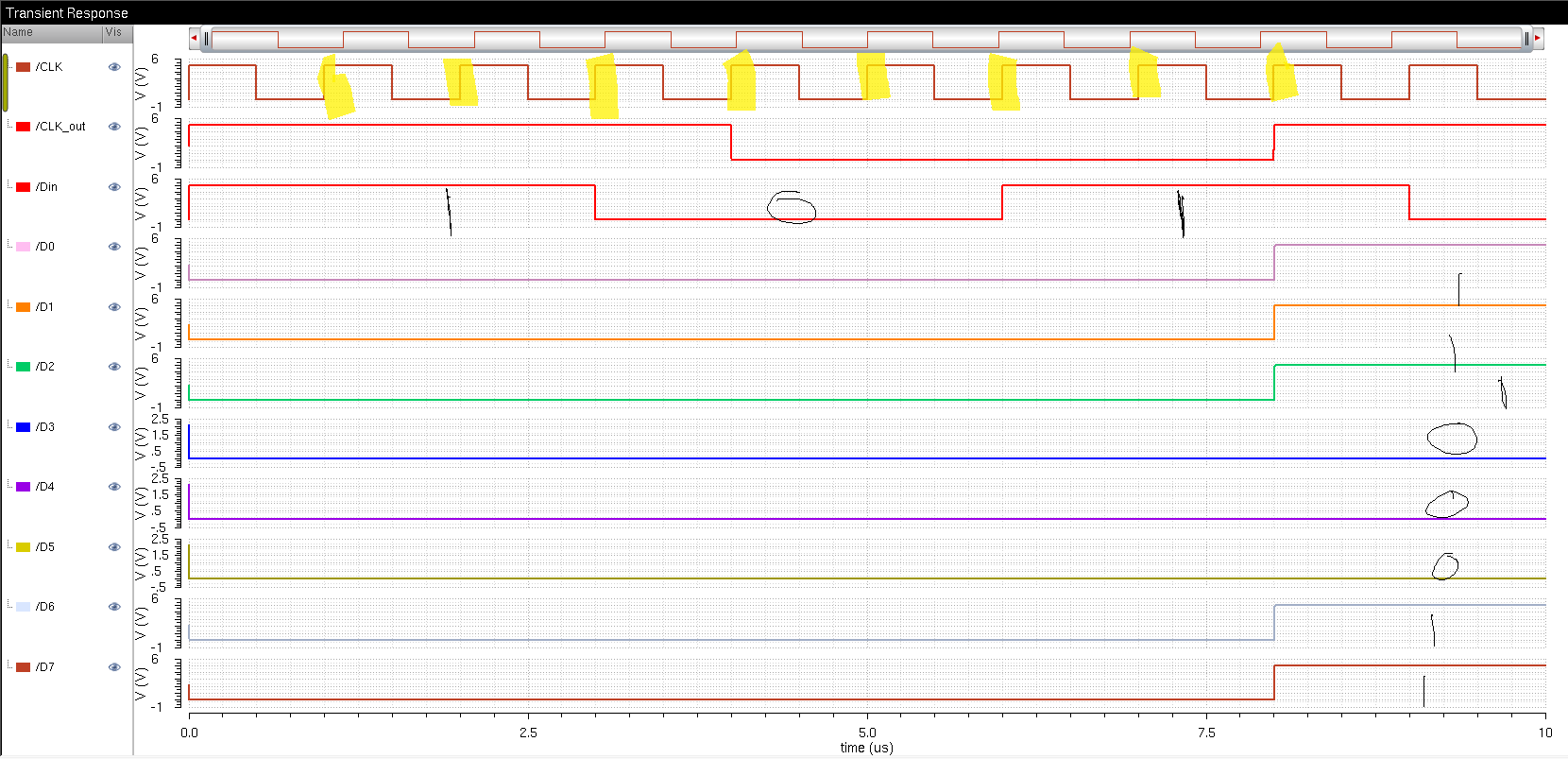 |
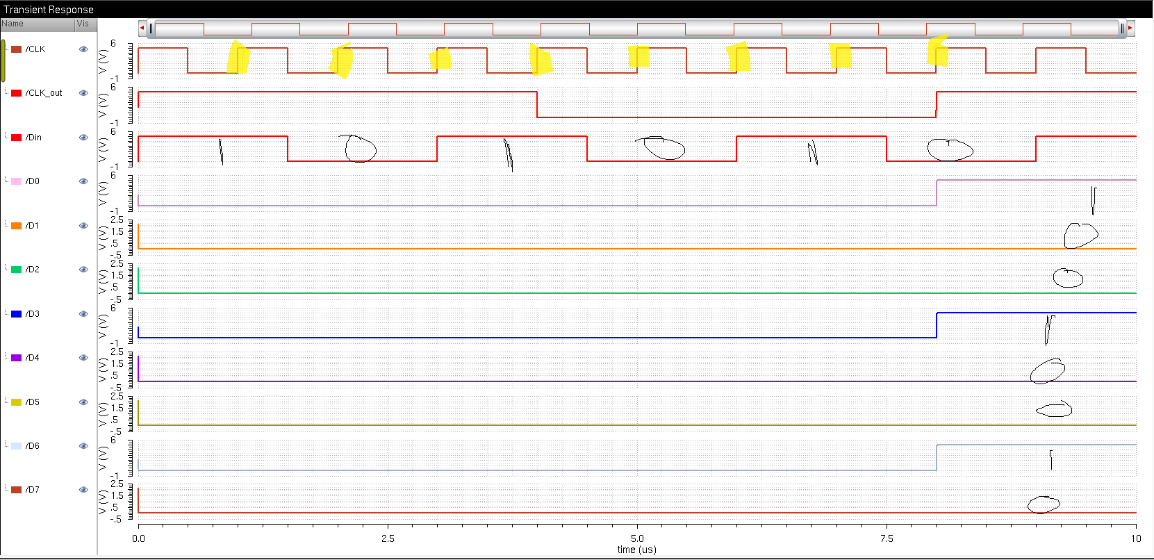 | When the CLK is on a rising edge the value of Din is inputted. The first value goes to D7 and so on.
First Plot Output :10101010
Second Plot: Output:1111111
Third Plot Output:11000111
Fourth Plot Output: 01001001
The CLK edges are in yellow. |
Layouts for Inverter, Transmission Gate, D-Flip Flop, CLK/8, Serial to Parallel Converter
| Inverter Schematic | Inverter DRC |
 | 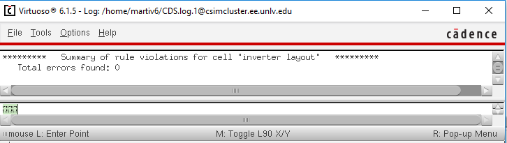 |
| Inverter Layout | Inverter LVS |
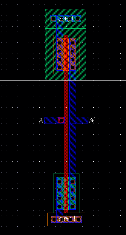 |  |
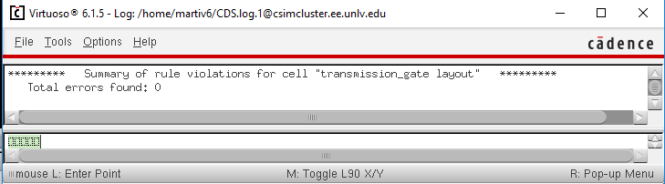
| Transmission Gate Schematic | Transmission Gate DRC |
 |  |
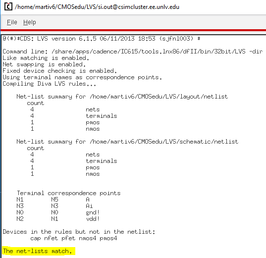
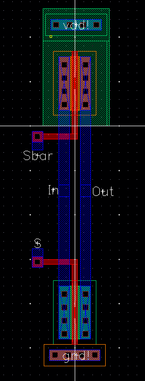
| Transmission Gate Layout | Transmission Gate LVS |
 |  |
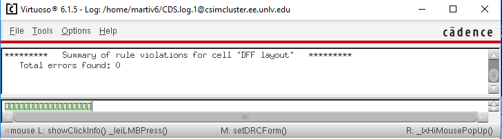
| D-Flip Flop Schematic(uses TG and inverters to get outputs of Q and Qbar) | D-Flip Flop DRC |
 |  |
| D-Flip Flop Layout | D-Flip Flop LVS |
 |  |
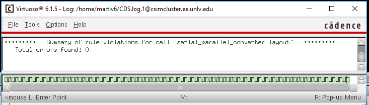
| CLk/8 Schematic | CLK/8 DRC |
| 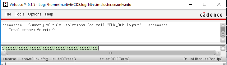 |
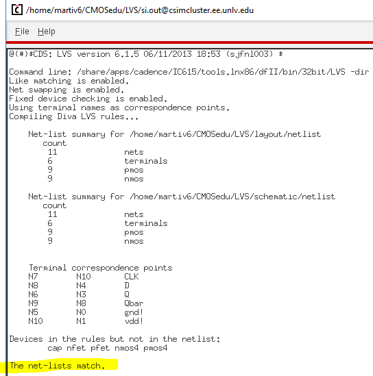
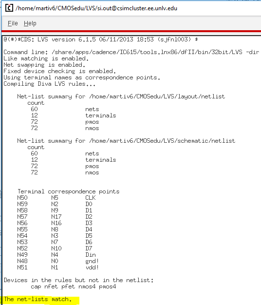
| CLK/8 Layout ( takes the CLK that is inputted and Divides it by 8) | CLK/8 LVS |
 |  |
| D-Flip Flops no CLk/8 Schematic | D-Flip Flops no CLk/8 DRC |
|  |
| D-Flip Flops no CLk/8 Layout | D-Flip Flops no CLk/8 LVS |
 |  |
| Serial
to Parallel Converter Schematic( takes an input and runs it through 8 D
Flip Flops and inputs the CLk into the CLK/8 which is then fed to the
other 8 DFF) | Serial to Parallel Converter DRC |
|  |
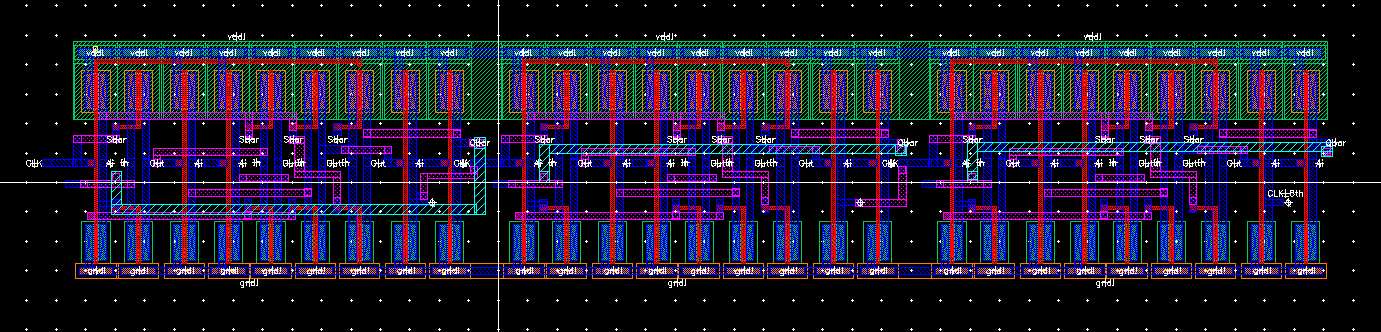
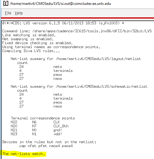
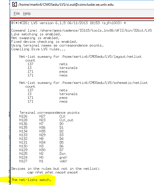
| Serial to Parallel Converter Layout | Serial to Parallel Converter LVS |
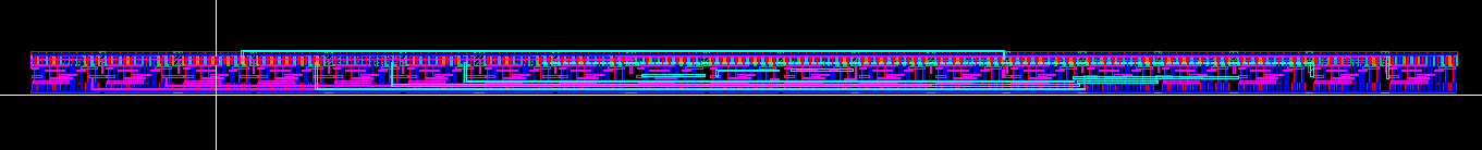 |  |
ZOOMED IN LAYOUT OF SERIAL TO PARALLEL CONVERTER
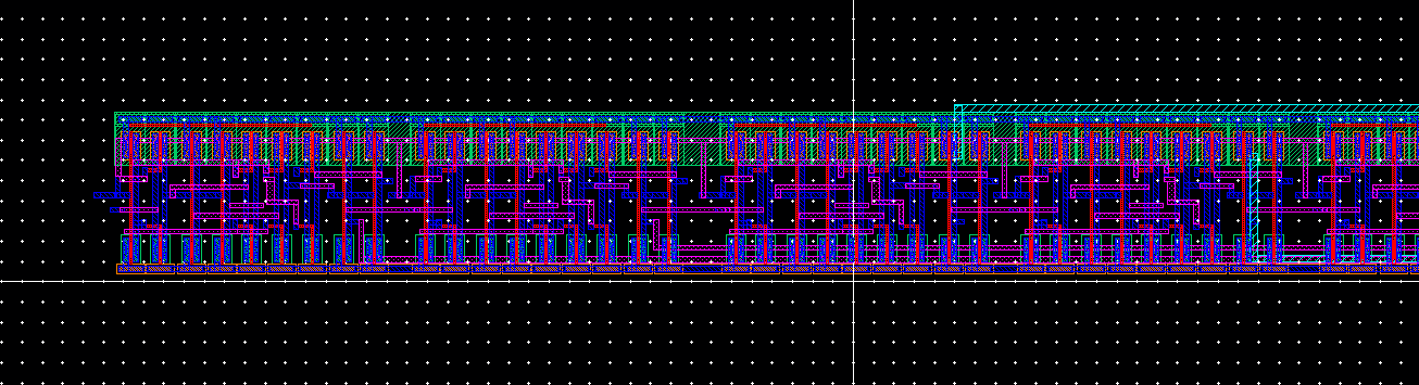 | 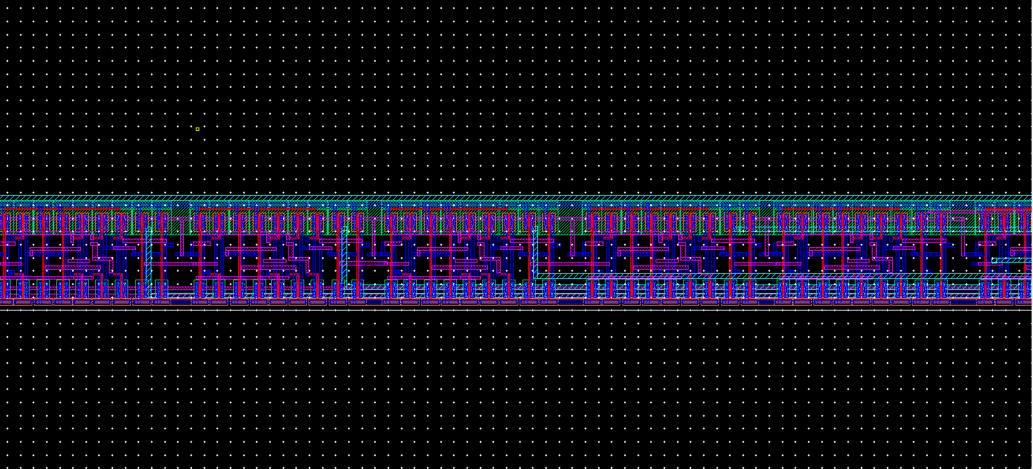 | 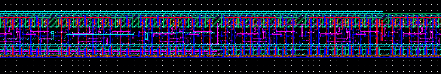 | 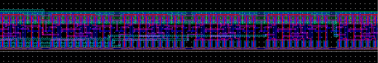 |  |
| The first two images are 8 D-Flip Flops (they are for the serial inputs) | The inputs go throught the 8 D-Flip Flops | This is where the CLK/8 is in the Layout then goes to the other D Flip Flops with the right CLK speed | The remain images are the outputs of the Serial to Parallel converter at the right ClK speed from D7-D0 | |
Files are found here
Return to Labs