Lab 2 - EE 421L
Design of a 10-bit digital-to-analog converter (DAC)
Authored
by Victor Martinez
martiv6@unlv.nevada.edu
September 9, 2018
Lab
description: We'll use n-well resistors to implement a 10-bit DAC.
Prelab:
- Make sure you understand how the input voltage, Vin, is related to B[9:0] and Vout.
- In
your lab report: 1) provide narrative of the steps seen above, 2)
provide, and discuss, simulation results different from the above to
illustrate your understanding of the ADC and DAC, 3) explain how you
determine the least significant bit (LSB, the minimum voltage change on
the ADC's input to see a change in the digital code B[9:0]) of the
converter. Use simulations to support your understanding.
- Backup your webpages and design directory.
Setting up Lab 2:
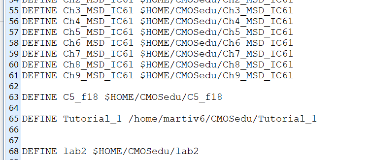
We need to upload the zip file, lab 2, to the design directory on the server that Cadence is on.
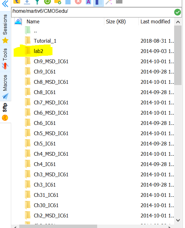
Unzip this directory and add, to your cds.lib in the design directory, the following statement - DEFINE lab2 $HOME/CMOSedu/lab2

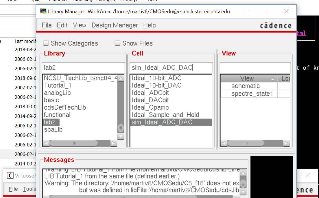
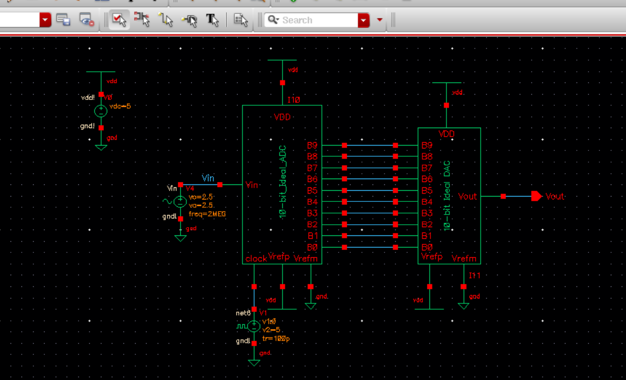
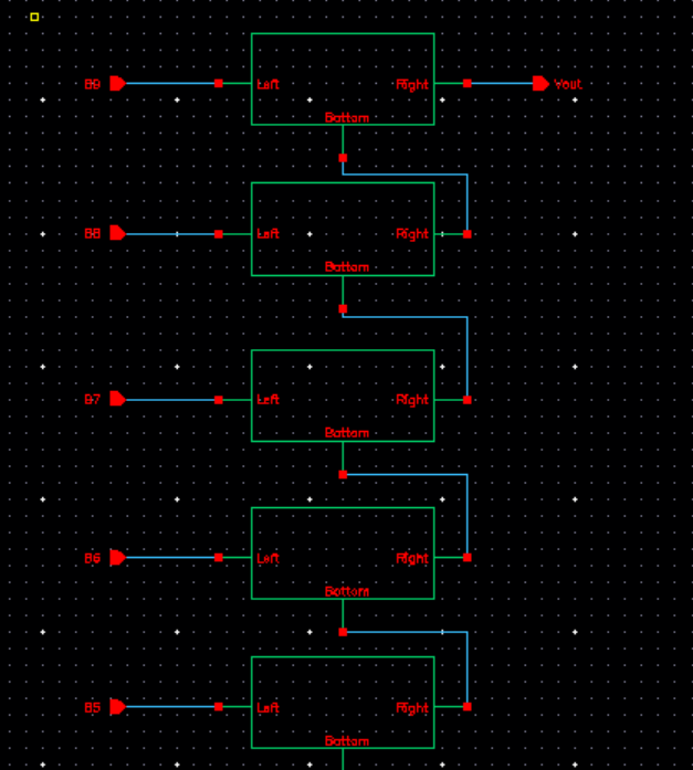
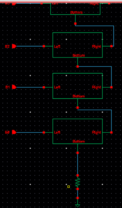
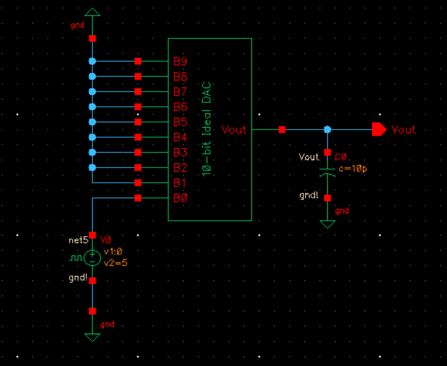
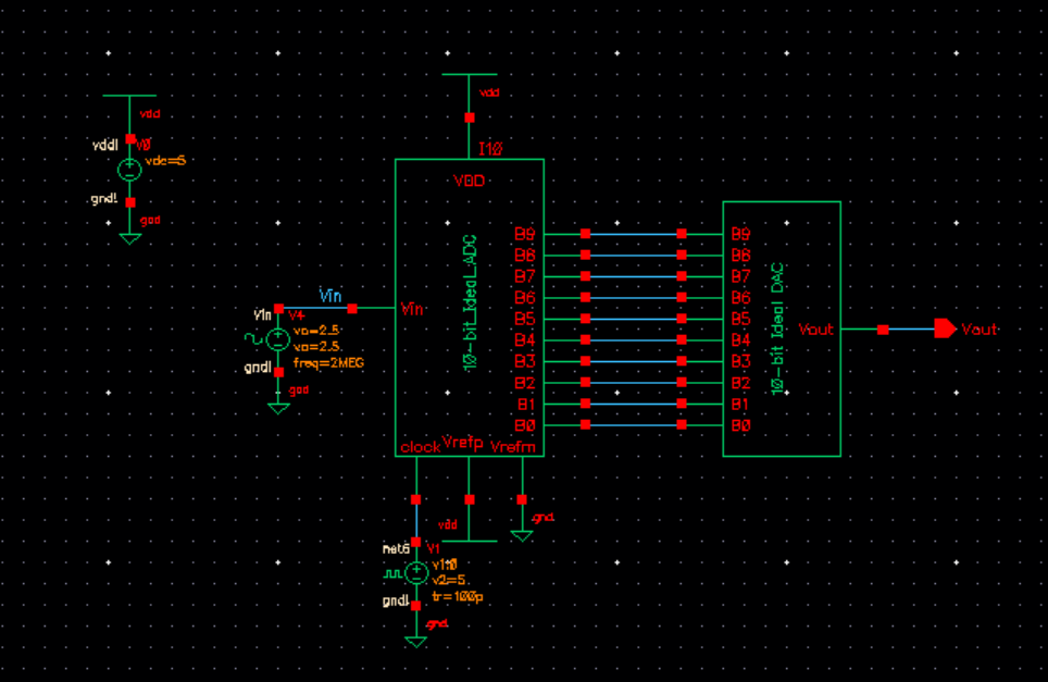
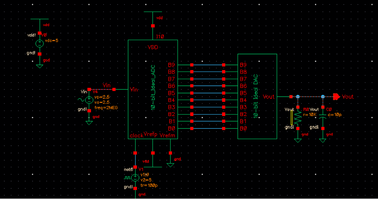
Open the schematic view of the cell sim_Ideal_ADC_DAC. Then run the simulation.
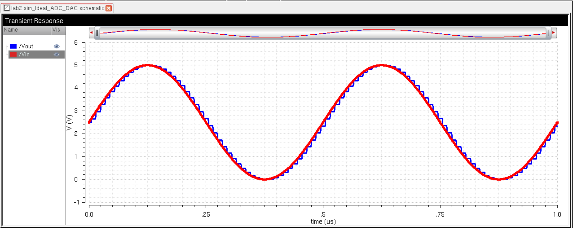
Schematic of sim_Ideal_ADC_DAC
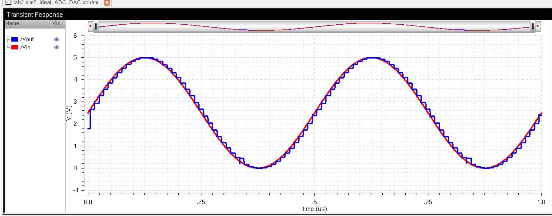
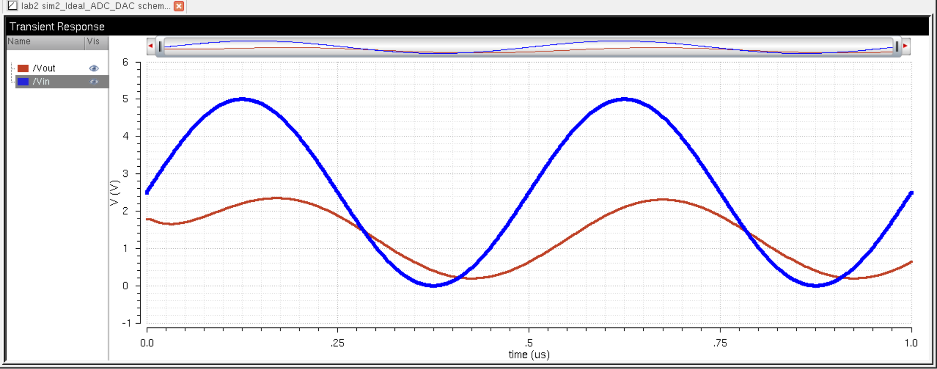
Simulation of sim_Ideal_ADC_DAC
Simulation to show what is the LSB( least significant bit )
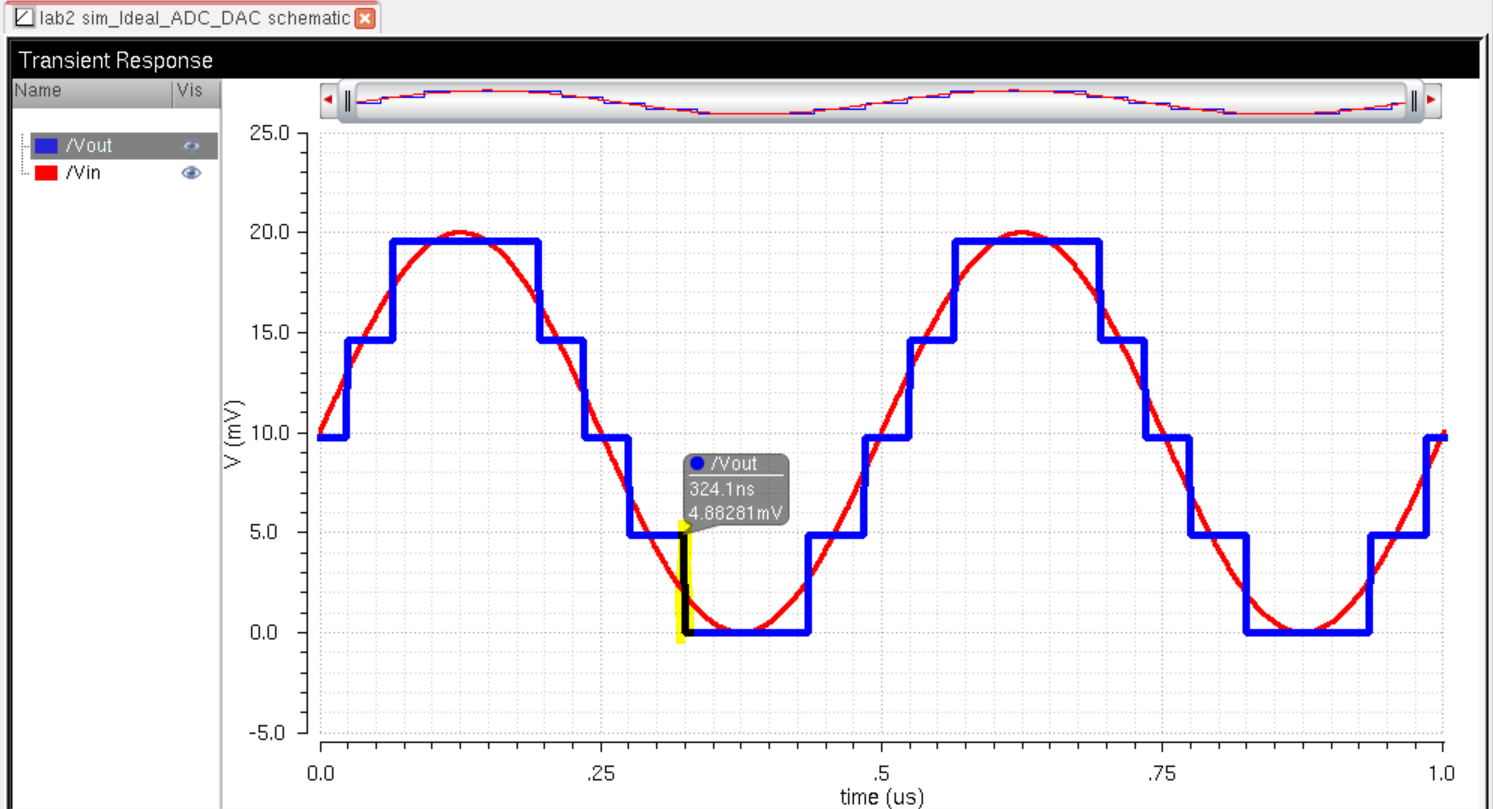
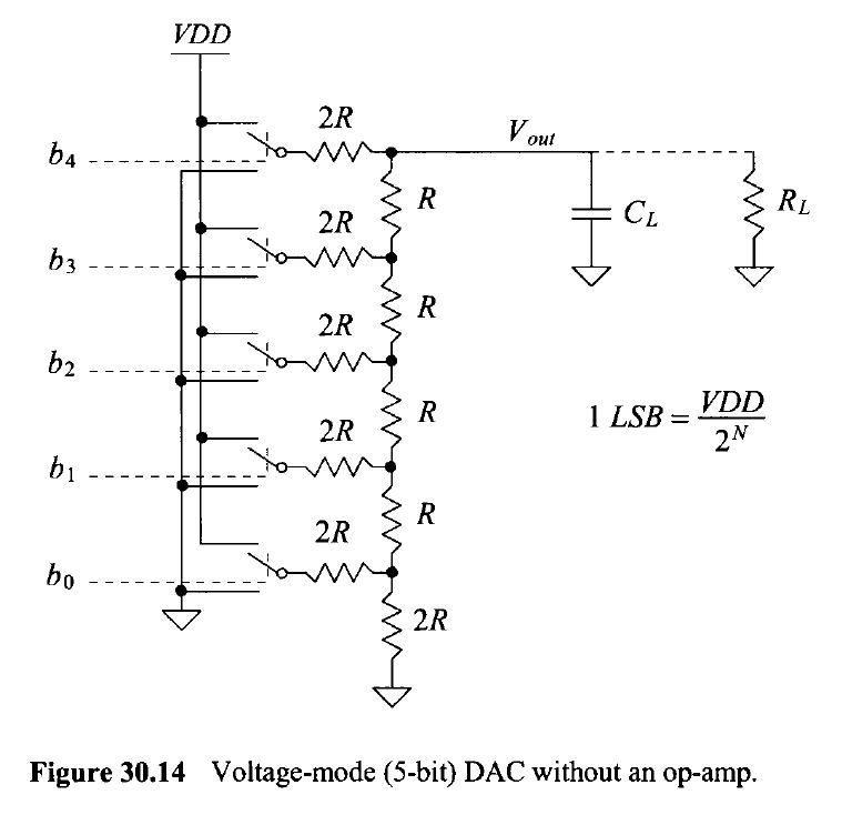
From Figure 30.14,
we find out that the calculate LSB you divide the VDD by 2^N which in
this case is 10, the number of bits in out DAC. We get around 4.88 mV
which is what is comfirmed above.
Lab:
Using the DAC from the book
Designing 10-bit DAC using N-well R of 10k
After
creating the schematic whihc is two resistors in series with one in
parallel, I save and check. I made a symbol of the resistors.
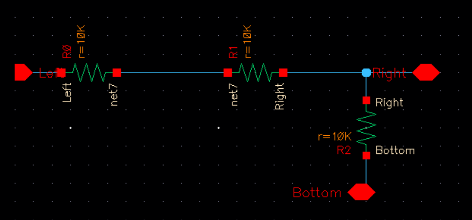
Creating the DAC
The Delay
DAC with no Load
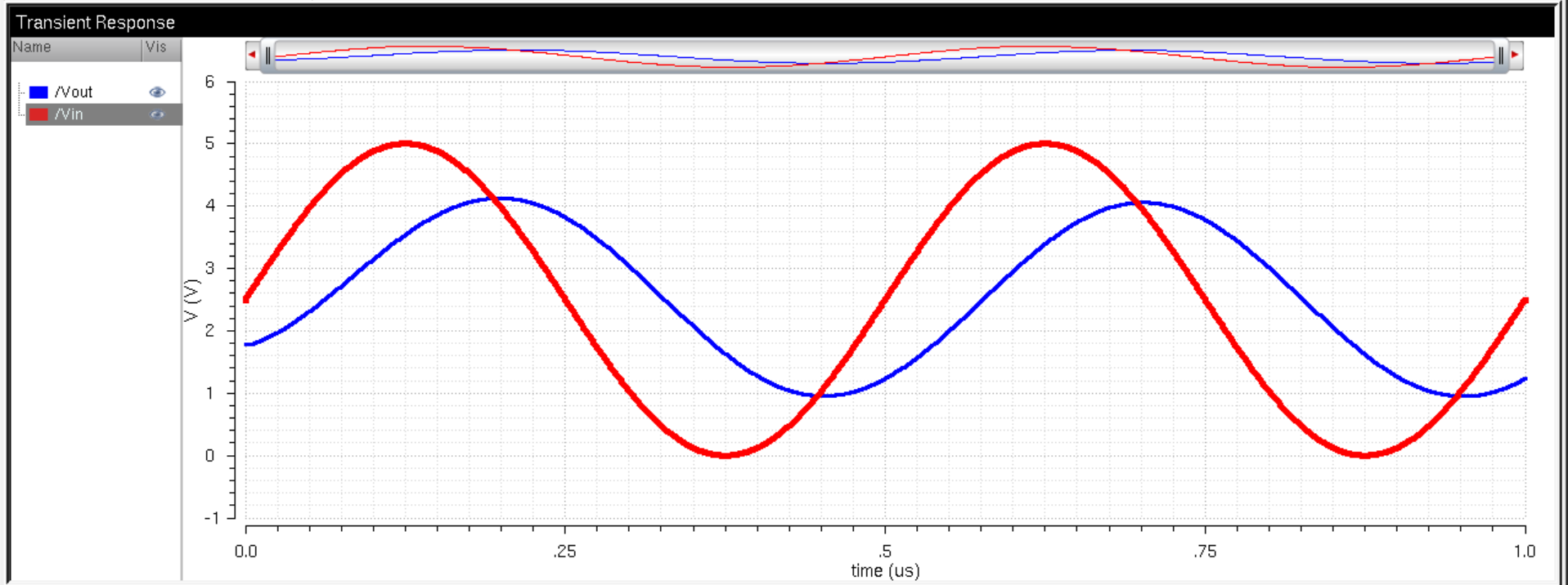
DAC with 10pF load
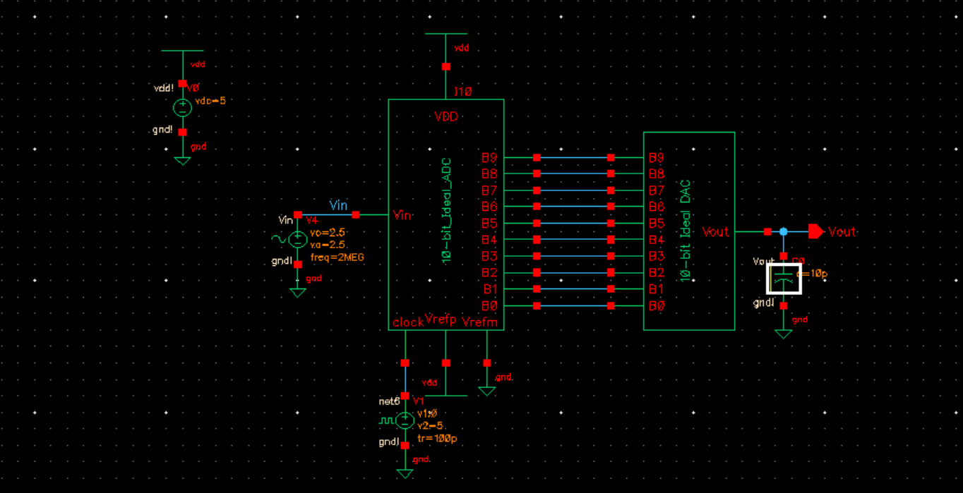
DAC with 10k and 1pF
In
a real circuit, if the switch resistance was not small compared to R,
the equivalent resistance of the entire DAC would not be R, and we
would need to recalculate the resistance of the DAC in order to match
the load resistance and maximize the output with a load connected.
- If
you have simulation convergence problems you can force the simulation
to converge by going to, in the ADE, Simulation -> Options ->
Analog
- Set the values as seen below
- relative tolerance, reltol, of 10% (= 1e-1)
- voltage absolute tolerance, vabstol, of 100 mV (= 1e-1)
- current absolute tolerance, iabstol, of 1 mA (= 1e-3)
I did have problems with simulation convergence, and needed to force the sims using the values above.
Backing up Lab

Return to Labs