Project - ECE 421L
-Inputs: Din ;
Clock_in
-Outputs: D0-D7; Clock_out
-10 Mbits/s --> 1.25 MWords/s.
First Half:
Serial-to-parallel converter schematics for designs as well as operation report
(including simulations).
The individual
components used for the design will be shown first, leading up to the
converter’s design itself:
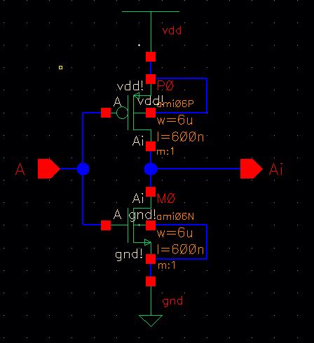
Inverter:
|
Schematic |
|
|
Symbol |
|
Transmission
Gate:
|
Schematic |
|
|
Symbol |
|
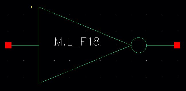
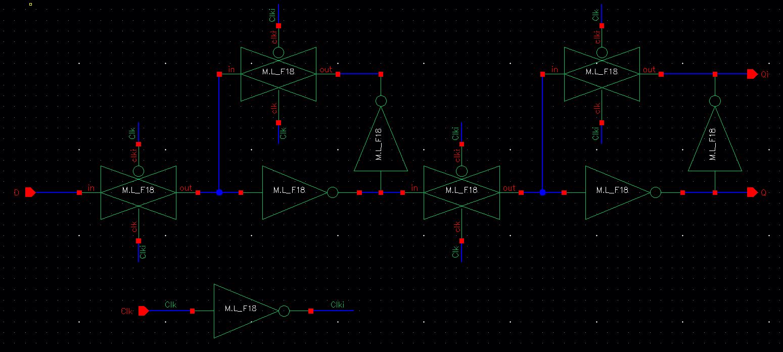
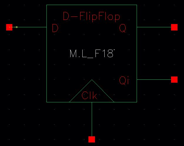
D Flip-Flop:
|
Schematic |
|
|
Symbol |
|
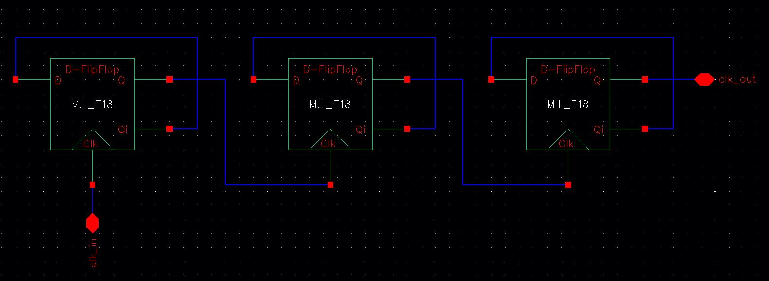
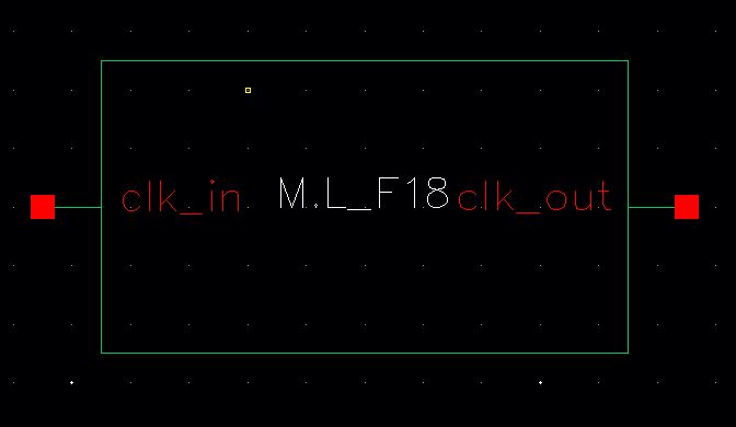
Reduced Clock:
|
Schematic |
|
|
Symbol |
|
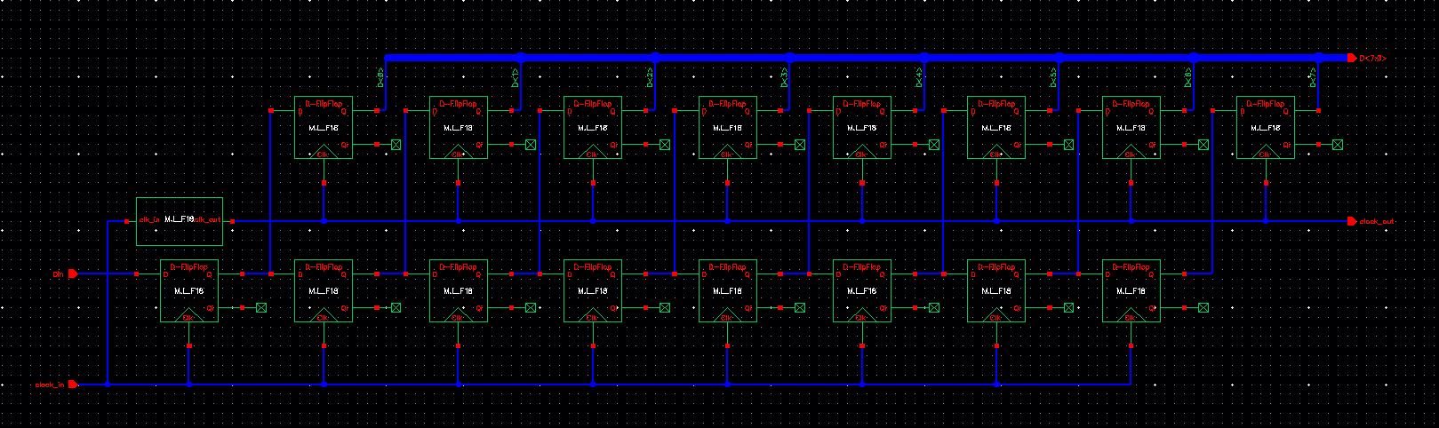
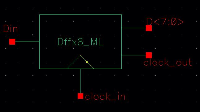
Serial-Parallel
Converter (using symbols listed above):
|
Schematic |
|
|
Symbol |
|
Schematic 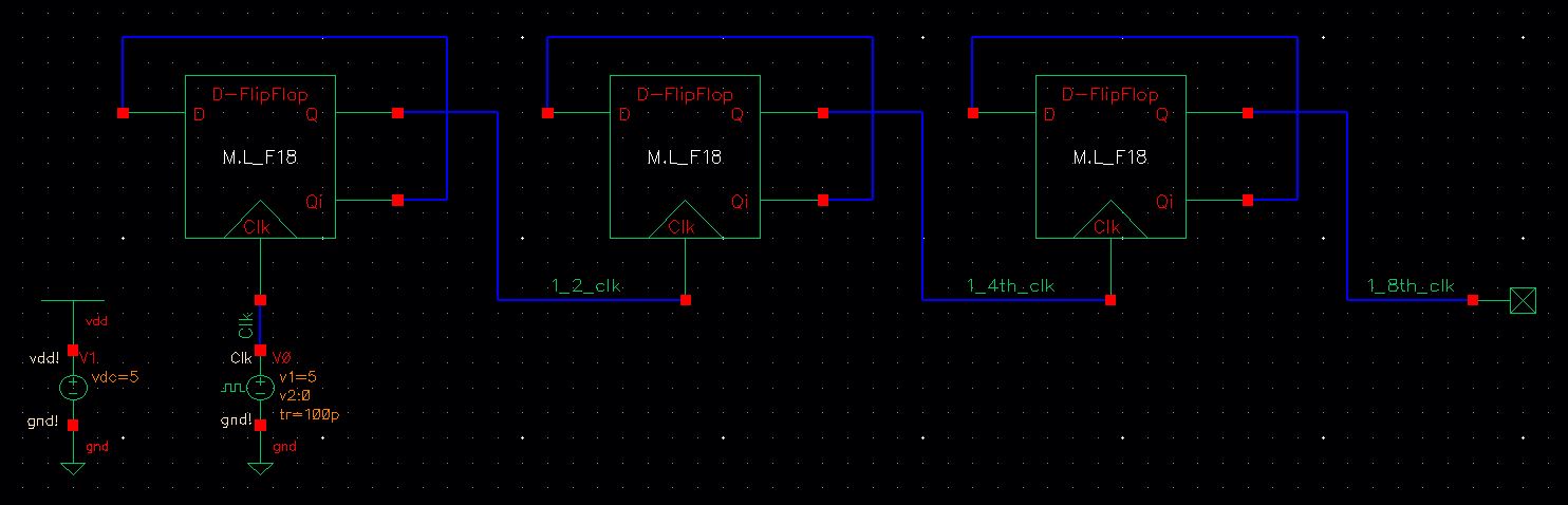
Simulation 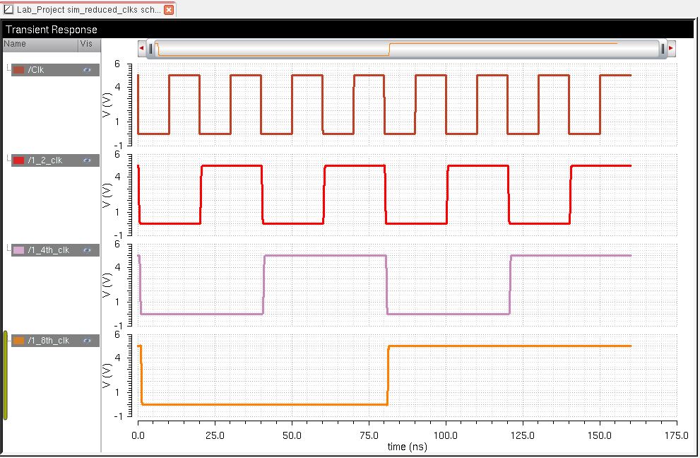
| Schematic | 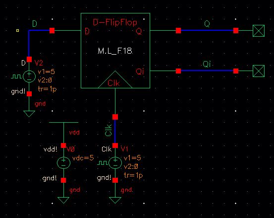 |
| Simulation | 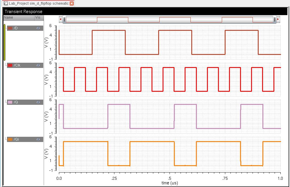 |
| Schematic | 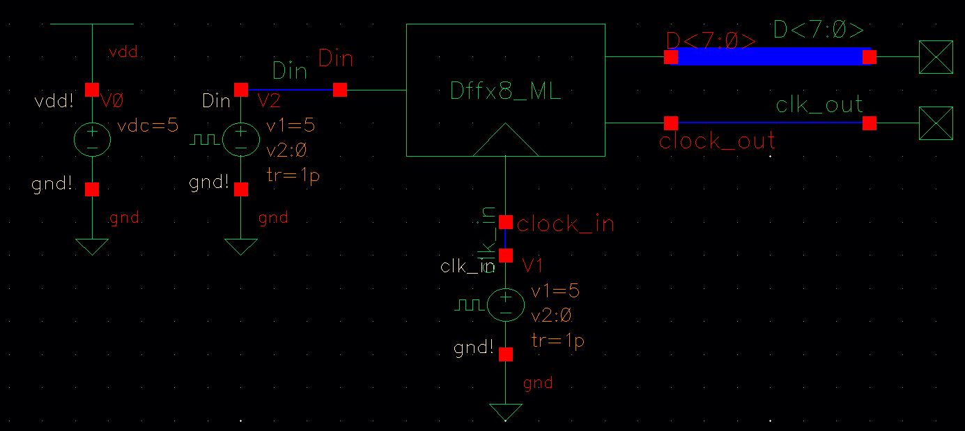 |
| Simulation | 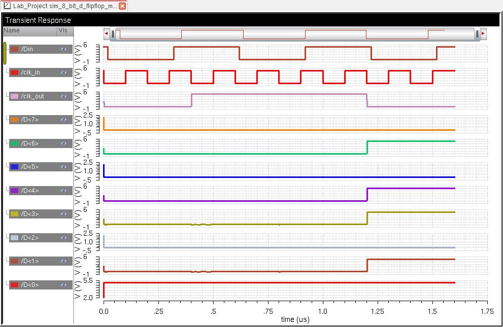 |
For the simulations regarding the serial-to-parallel converter, I fed an 8-bit code of 0101-1011 through the series input. As the simulations show above, the output displays an 8-bit word reading 0101-1011 when the output clock from the reduced clock circuit triggers, showing that the clock registered all 8 bits from the series input.
The files used for making these simulations and designs can be found in the following link: Proj
----------------------------------------------------------------------------------------------------------------------------------------------------------------------------------
----------------------------------------------------------------------------------------------------------------------------------------------------------------------------------
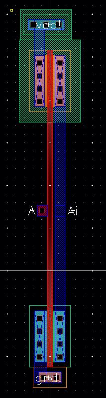
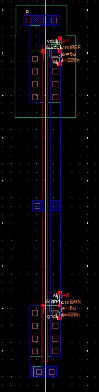
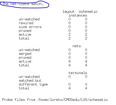
Each individual component for the serial-parallel converter has layout designs created for them. DRC checks and LVS's are run over each component design in order to ensure that they match up to the original schematics.
Inverter:
| Layout | Extracted | DRC | LVS |
 |  |  |  |
Transmission Gate:
| Layout | Extracted | DRC | LVS |
 |  |  |  |
D Flip-Flop:
| Layout | 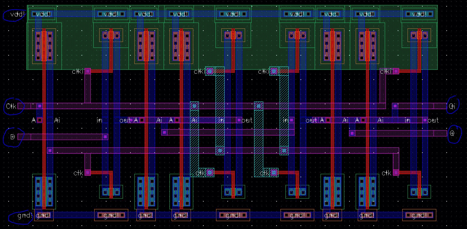 |
| Extracted | 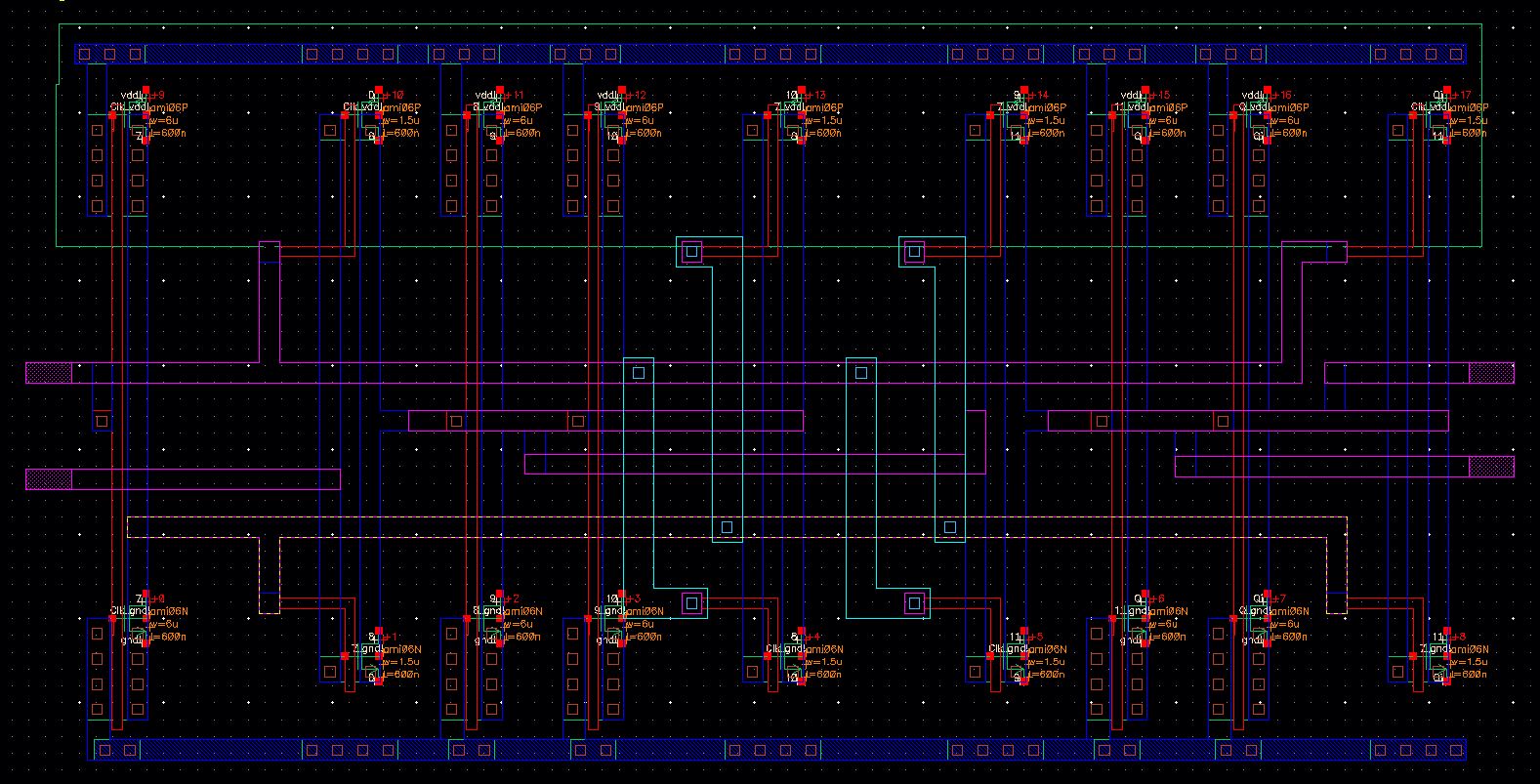 |
| DRC |  |
| LVS | 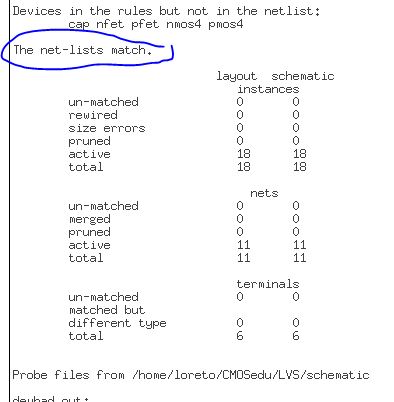 |
Reduced Clock:
| Layout | 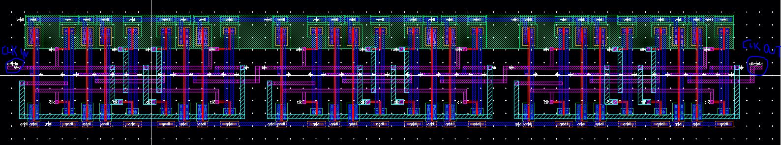 |
| Extracted | 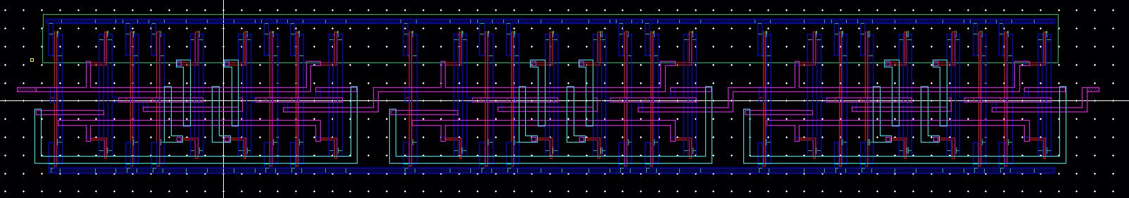 |
| DRC |  |
| LVS | 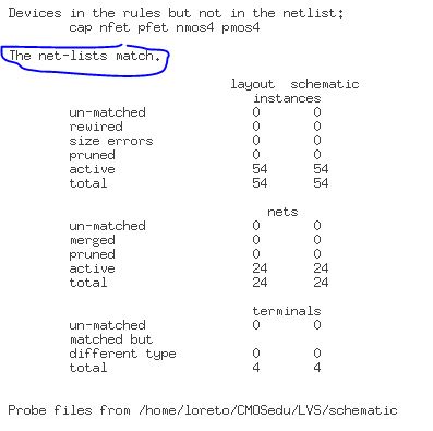 |
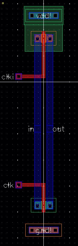
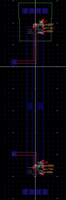
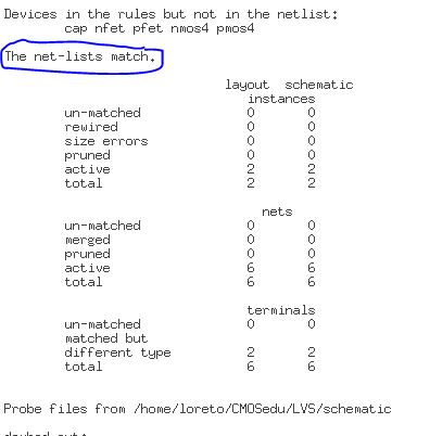
Serial-Parallel Converter:
| Layout | 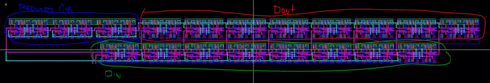 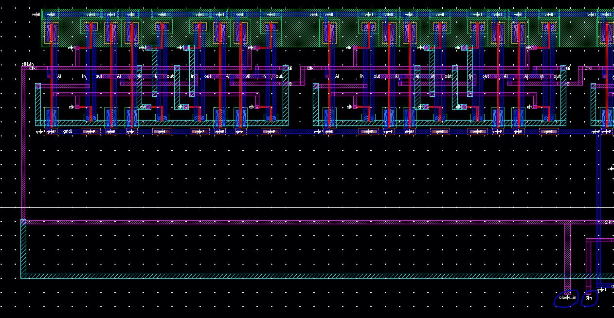 *Note: This image shows the clock_in and Din input pins for the whole design. The clock connects to the bottom registers and the reduced clock module. 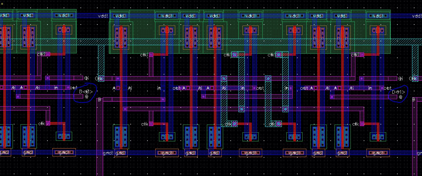 *Note: This image shows bits D<0> and D<1> for the output registers. Bits D<2> - D<7> Are positioned identically on the Q pins on their respective Flip-flops. |
| Extracted | 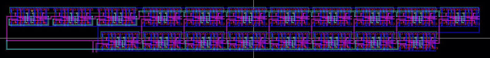 |
| DRC |  |
| LVS | 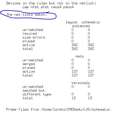 |
The files used for making these layouts and extracts can be found in the following link: Proj