Lab 8 - ECE 421L
Authored
by Michael Loreto, Ethan Tash, Rocky Yasuaki Gonzalez
Email: loreto@unlv.nevada.edu, tash@unlv.nevada.edu, gonzar14@unlv.nevada.edu
December 5, 2018
Lab 08: Generating a test chip layout for submission to MOSIS for fabrication.
----------------------------------------------------------------------------------------------------
Guidelines:
- One, or more if possible, course projects
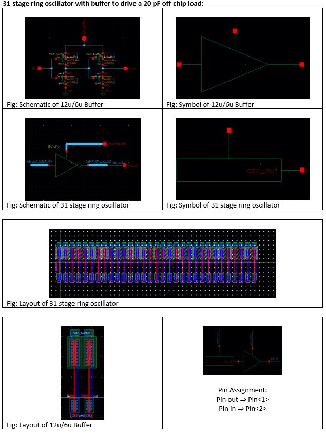
- A 31-stage ring oscillator with a buffer for driving a 20 pF off-chip load
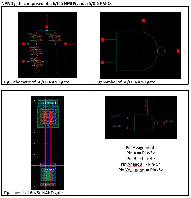
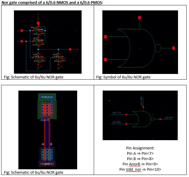
- NAND and NOR gates using 6/0.6 NMOSs and PMOSs
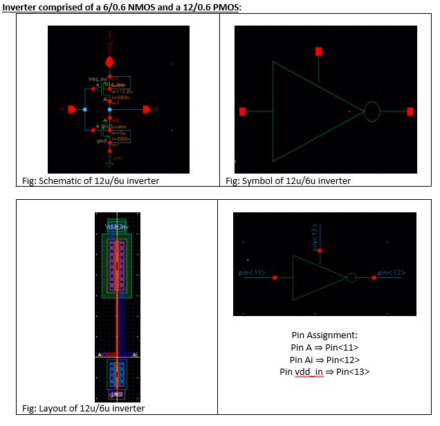
- An inverter made with a 6/0.6 NMOS and a 12/0.6 PMOS
- Transistors,
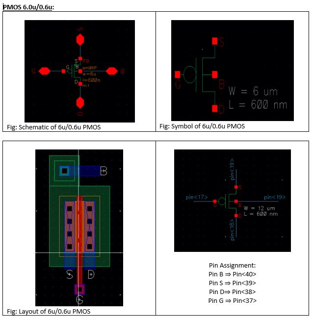
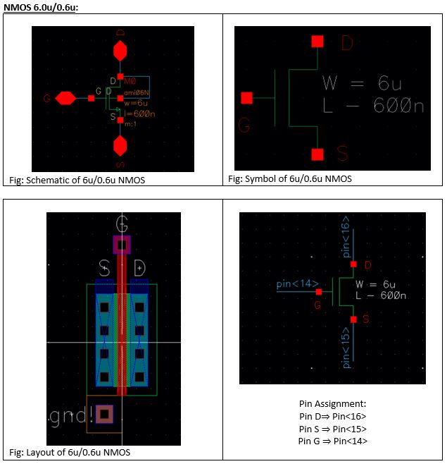
both PMOS and NMOS, measuring 6u/0.6u where all 4 terminals of each
device are connected to bond pads (7 pads + common gnd pad)
- Note
that only one pad is needed for the common gnd pad. This pad is used to
ground the p-substrate and provide ground to each test circuit
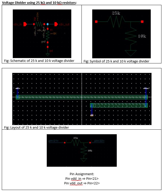
- Using
the 25k resistor laid out below and a 10k resistor implement a voltage
divider (need only 1 more pad above the ones used for the 25k
resistor)
- A 25k resistor implemented using the n-well (connect between 2 pads but we also need a common gnd pad)
- Whatever else you would like to fabricate to use the remaining pins on the chip
----------------------------------------------------------------------------------------------------
Individual components are designed and laid out below according to the instructions.
PMOS:
NMOS:
Inverter:
Voltage Divider (25k and 10k resistors)
NAND gate:
NOR gate:
31-stage ring oscillator:
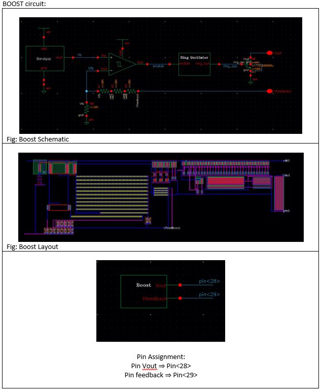
Boost Switching power supply:
----------------------------------------------------------------------------------------------------
Complete chip design: Schematic + Layout with all components included.
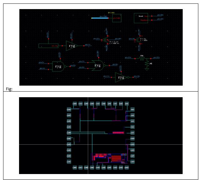
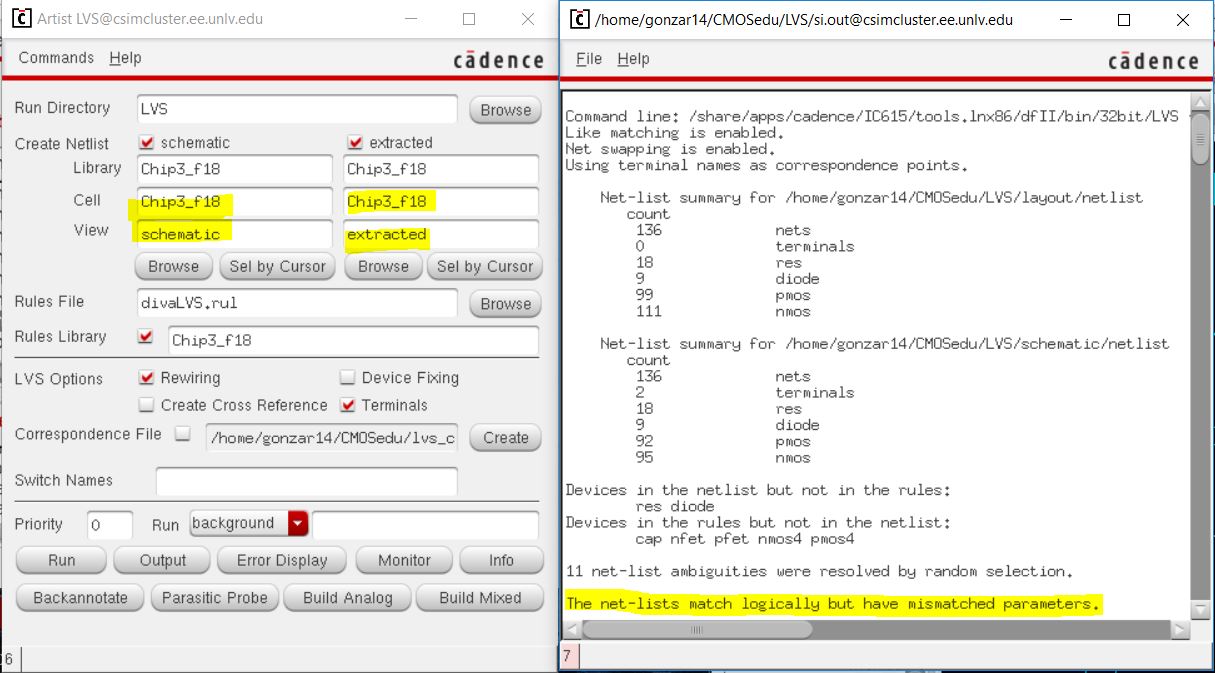
Layout successfully LVS checks with accomodating schematic.
----------------------------------------------------------------------------------------------------
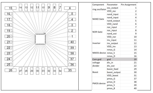
Pin assignments and details for the chip layout are organized in the table below for operational convenience.
Add
a return to the listing of your labs