Lab 7 - ECE 421L
4-bit Inverter:
| Schematic | 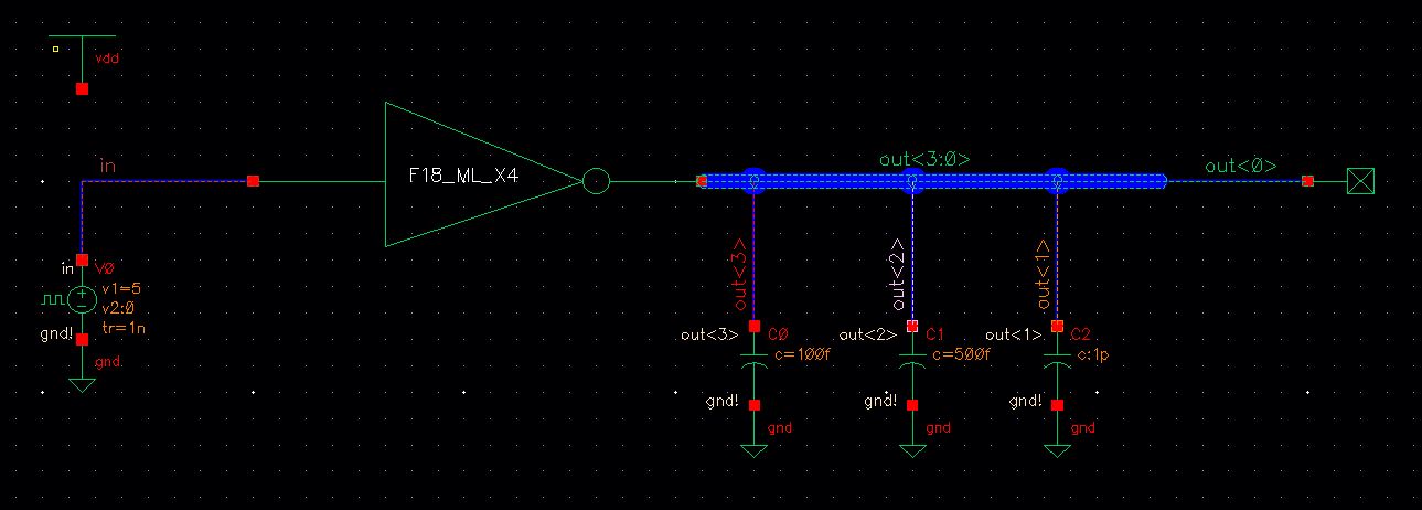 |
| Simulation |  |
-------------
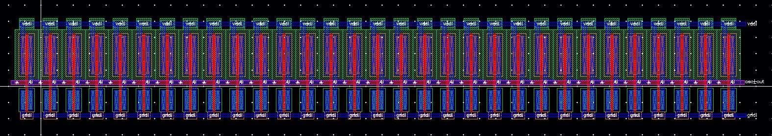
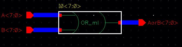
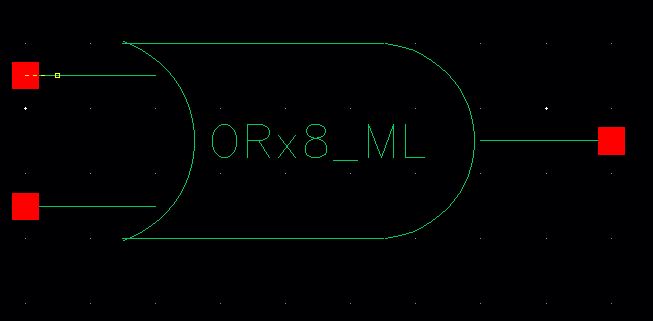
Create schematics and symbols for an 8-bit input/output array of: NAND, NOR, AND, inverter, and OR gates.
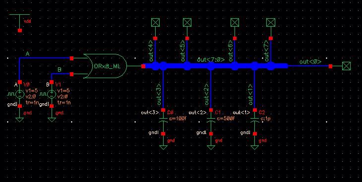
Provide a few simulation examples using these gates.
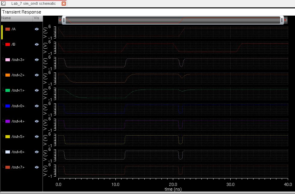
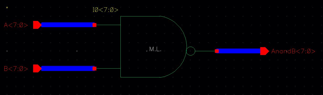
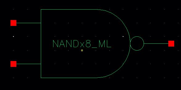
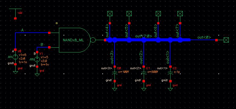
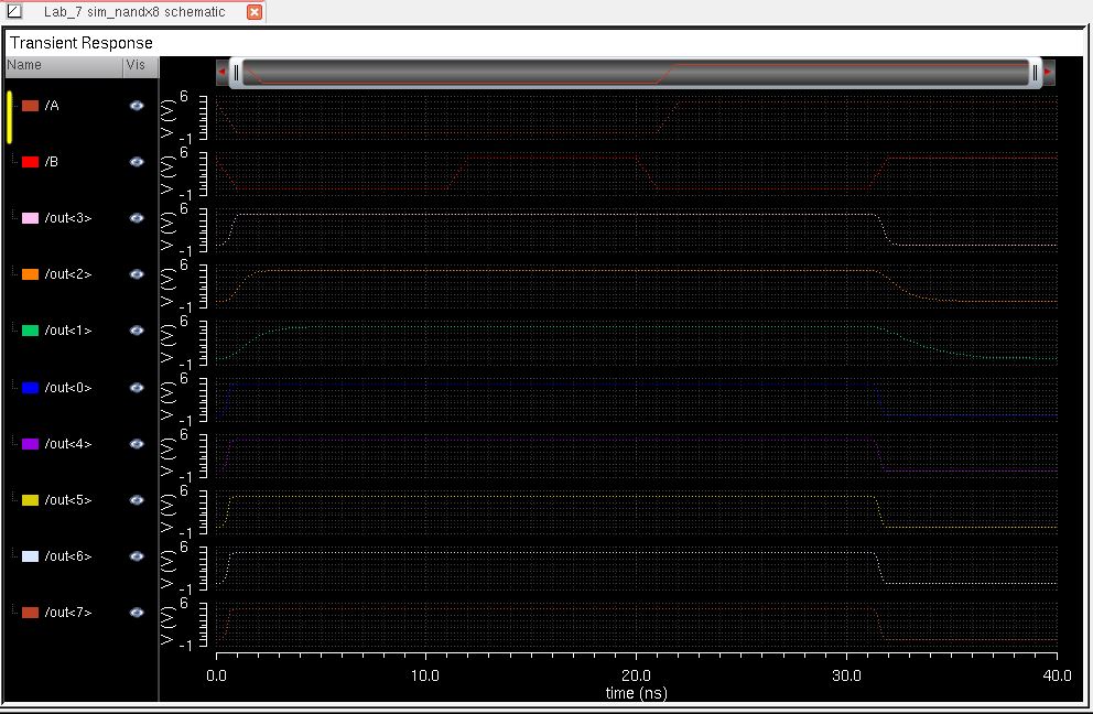
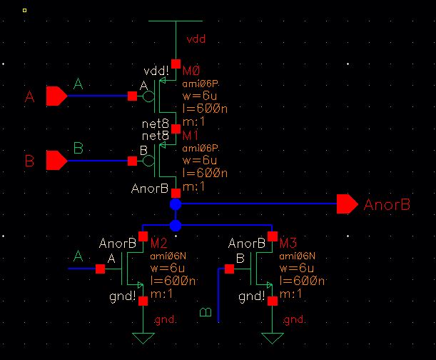
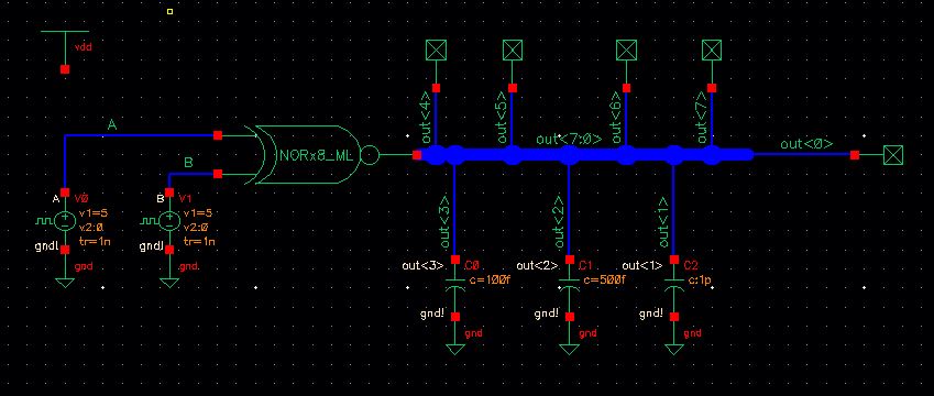
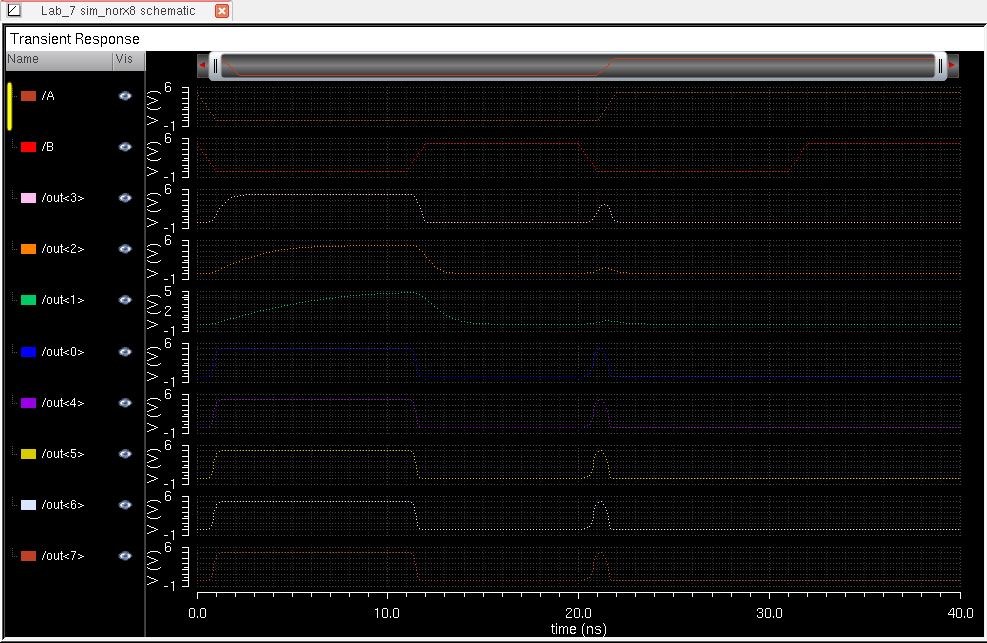
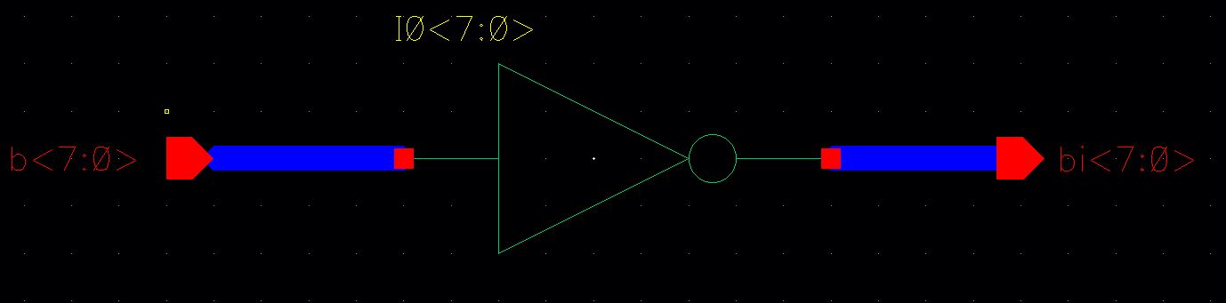
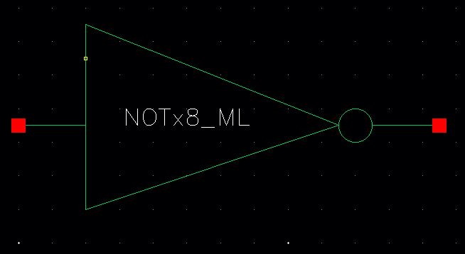
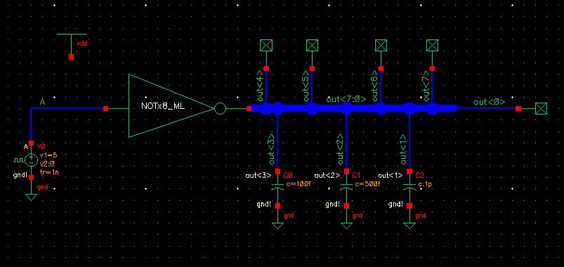
* For each of the gates, the inner schematics, the 8-bit symbol, the simulation schematic, and the simulation results are included.
-----------------------
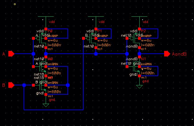
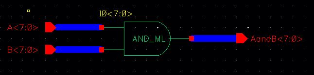
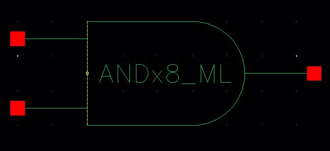
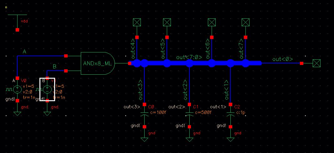
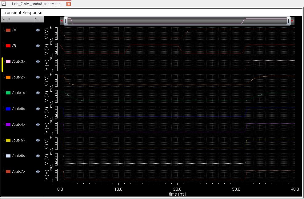
8-bit AND:
-----------------------------------------
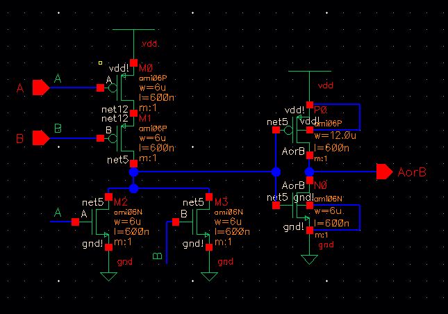
8-bit OR:
-------------------------------------------------
8 bit NAND:
-------------------------------------------
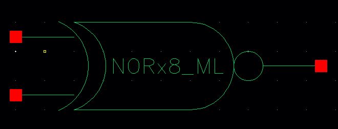
8 bit NOR:

----------------------------------
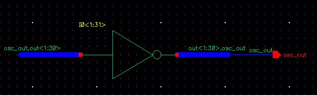
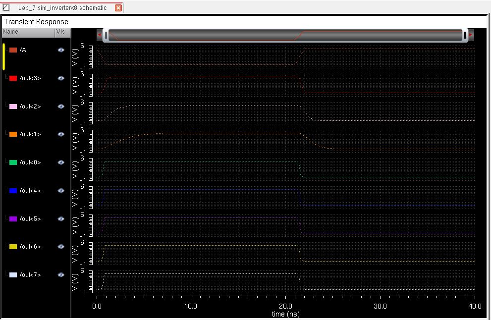
8-bit Inverter:
------------------------------------------------------------------------------
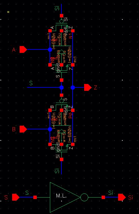
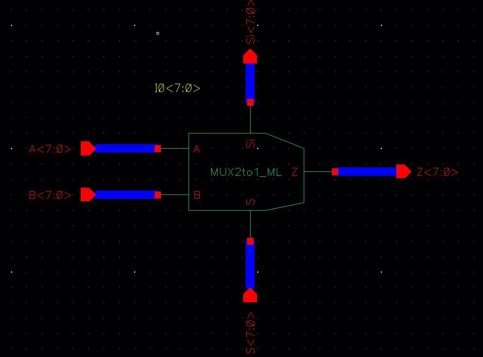
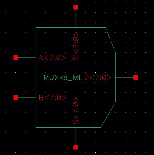
Create an 8-bit wide word 2-to-1 DEMUX/MUX schematic and symbol.
Include
an inverter in your design so the cell only needs one select input, S
(the complement, Si, is generated using an inverter).
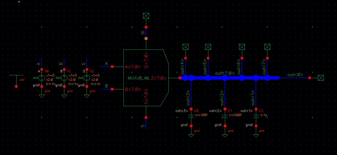
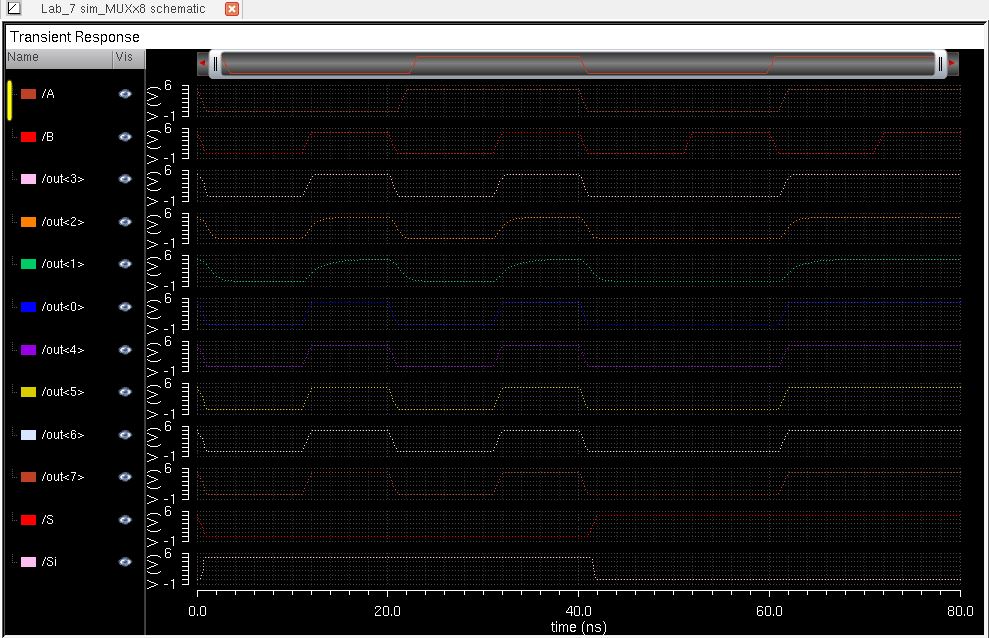
Use simulations to verify the operation of your design..
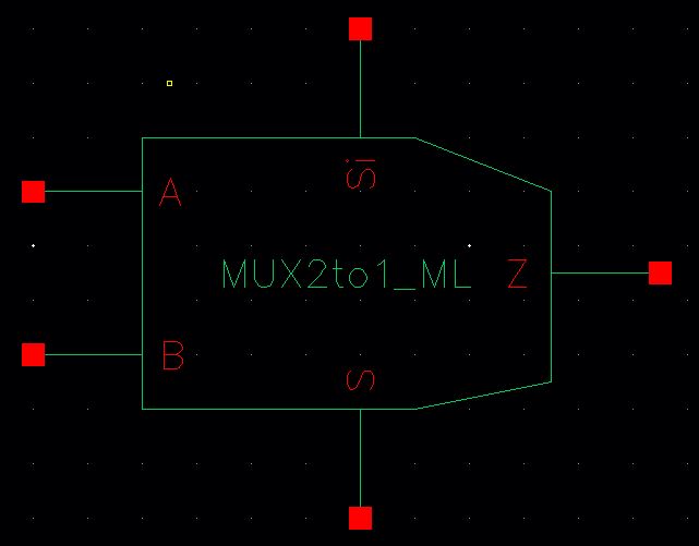
2 to 1 MUX:
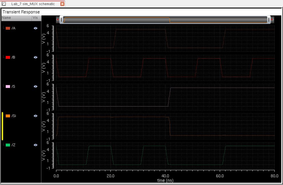
For the MUX Sim:
-When S = high, the values from A are shown in the output.
-When S = low, the values from B are shown in the output.
-------------
8-bit MUX:
-------------------------------------------------------------------------------------
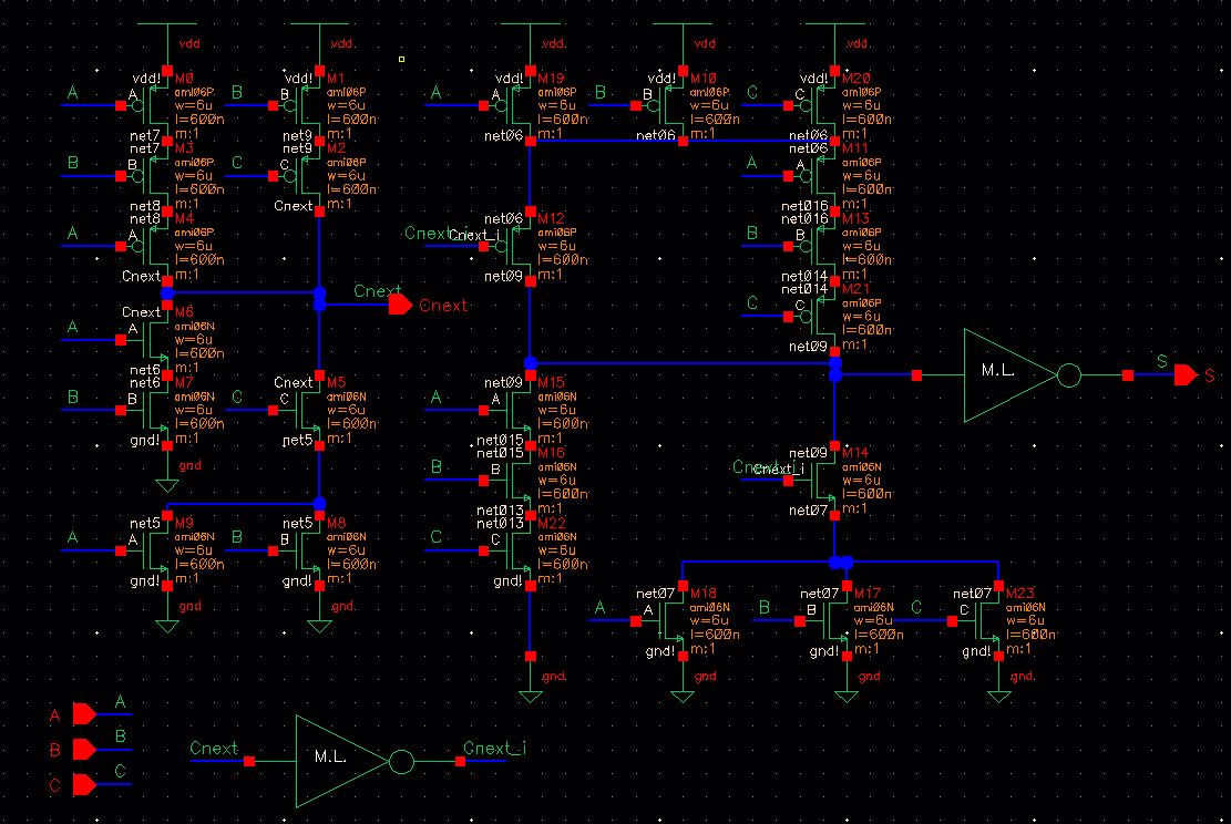
Draft the schematic of the full-adder seen in Fig. 12.20 using 6u/0.6u devices (both PMOS and NMOS).
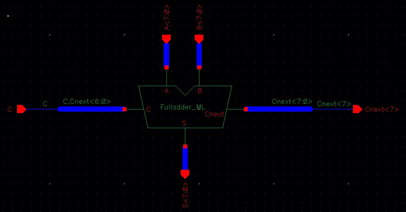
Create an adder symbol for this circuit (see the symbol used in lab6).
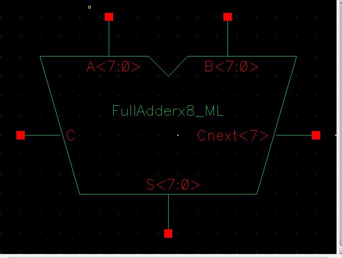
Use this symbol to draft an 8-bit adder schematic and symbol.
Simulate the operation of your 8-bit adder.
 *Symbol from inner schematic is shown in schematic for 8-bit adder.
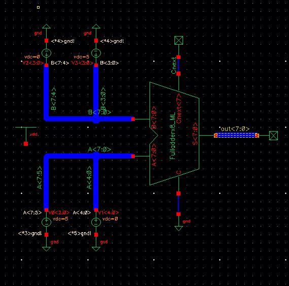
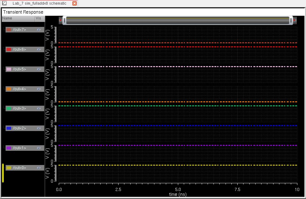
8-bit full-adder simulation:
A = 11100000
B = 00001111
S = 11101111
-----------------------------------------------------------------------------------
Lay out this 8-bit adder cell
Show that your layout DRCs and LVSs correctly.
Single Full Adder Layout/Extracted:
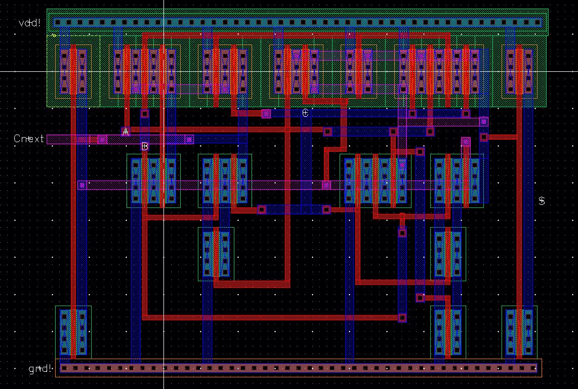

*Layout and extraction of the single full-adder design DRCs and LVSs correctly.
----------------------------------------------
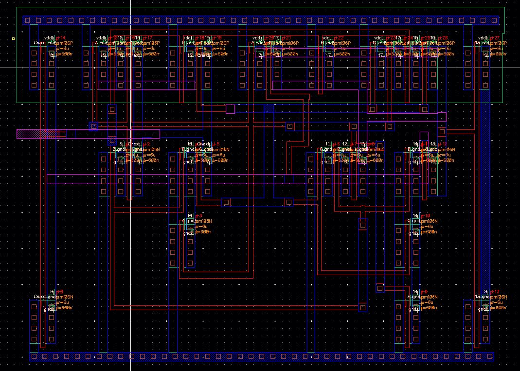
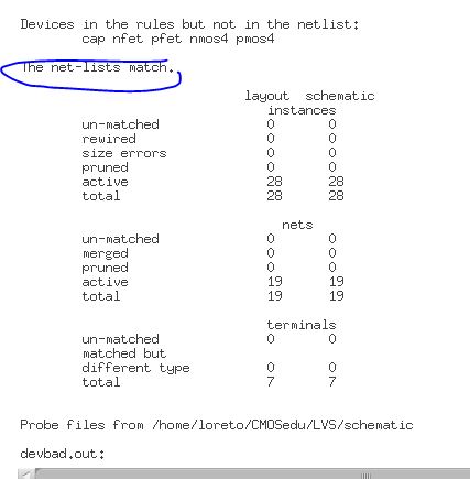
8-bit Adder Layout/extracted:
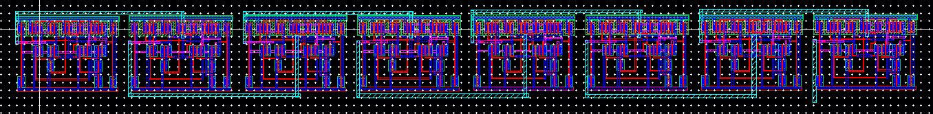
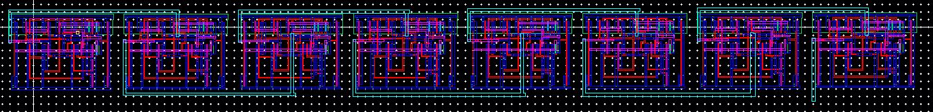

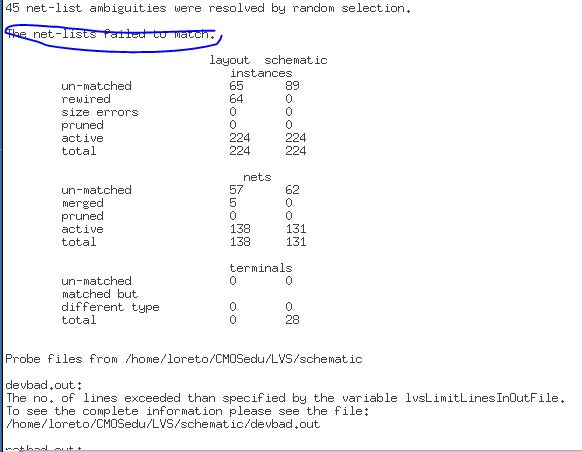
*Note: Numerous attempts were made to fix the matching issues for LVSsing the 8-bit full adder, but only a little progress was made.