Lab 5 - ECE 421L
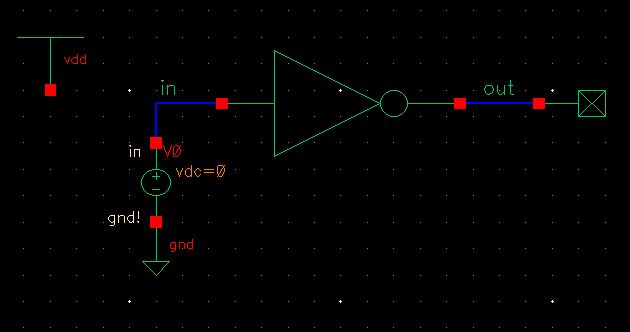
Results from Tutorial 3, I built and simulated the inverter as instructed in the tutorial.
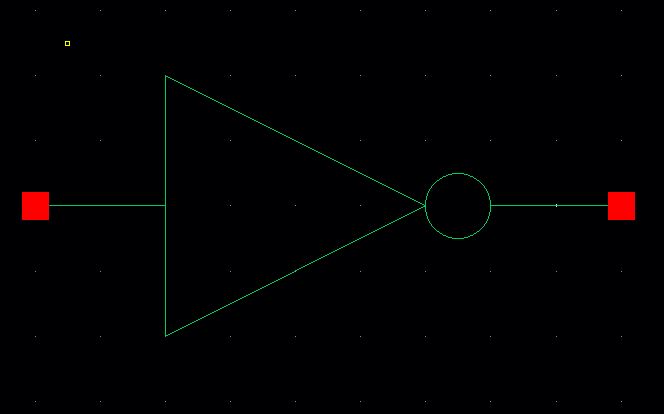
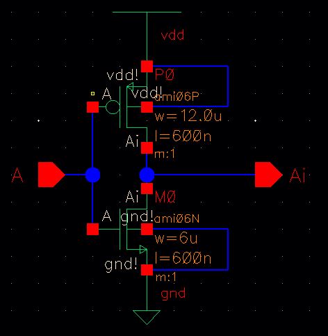
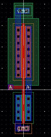
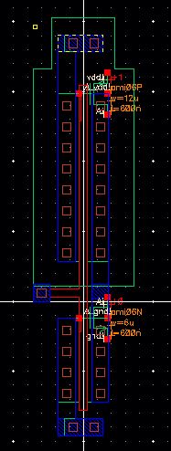
The schematic, layout, extracted, and symbol files of the Tutorial inverter are shown above.

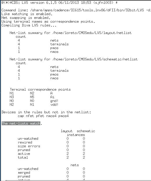
The DRC and LVS both checkout for my files.
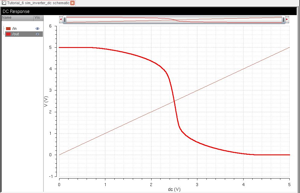
Upon instantiating my new inverter into a circuit schematic, the waveforms show that the inverter is behaving properly, as it inverts the signal according to the change in the input voltage.
Schematic 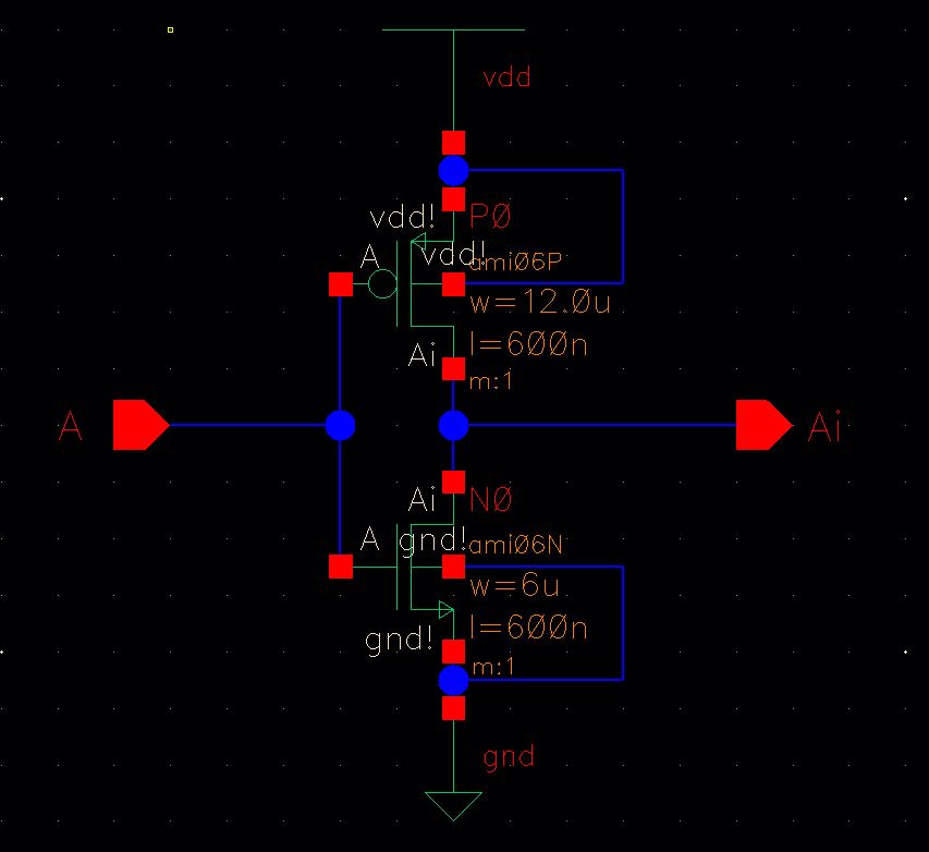
Layout 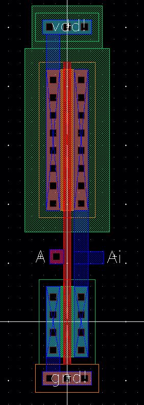
Extracted 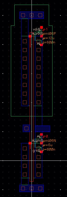
Symbol 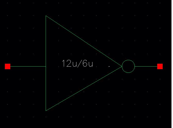
DRC 
LVS 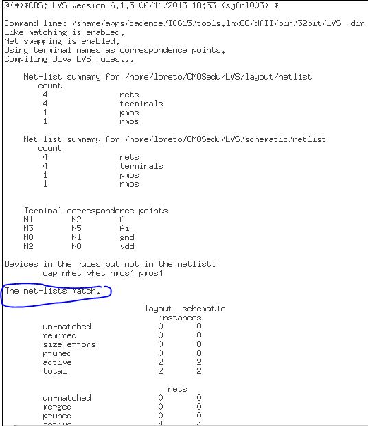
Schematic 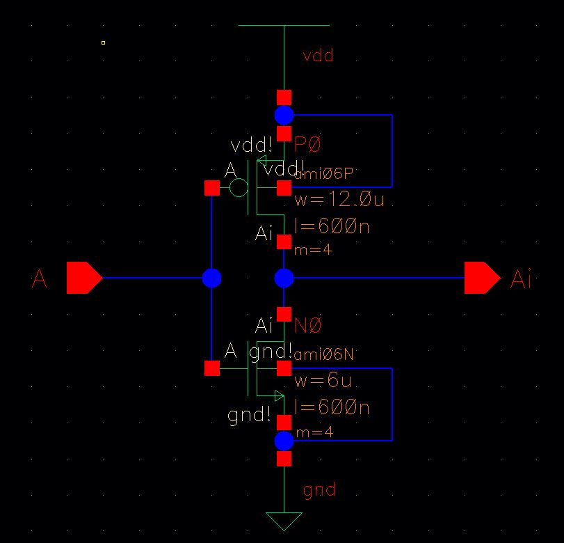
Layout 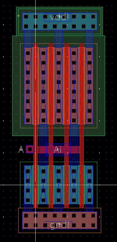
Extracted 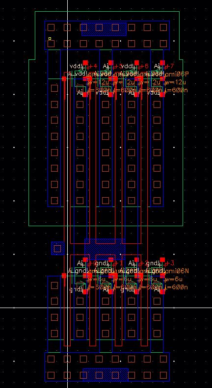
Symbol 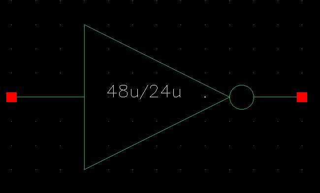
DRC 
LVS 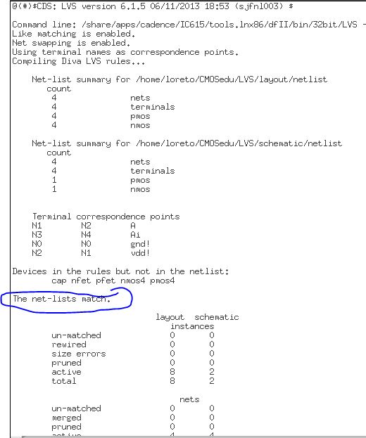
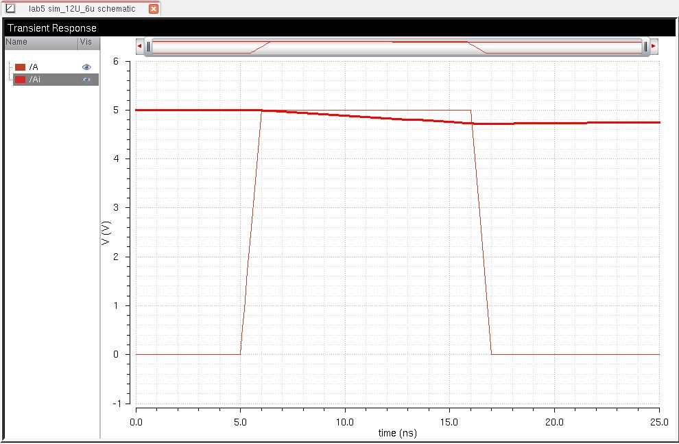
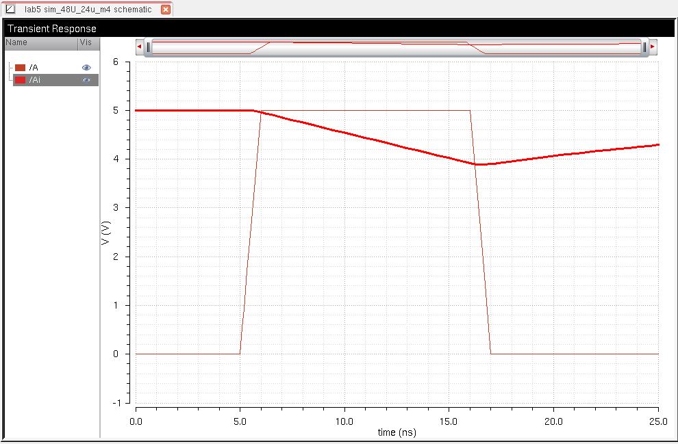
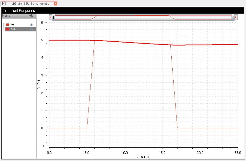
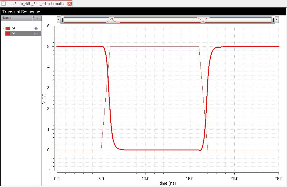
Load Schematic Simulation Comments 100 fF 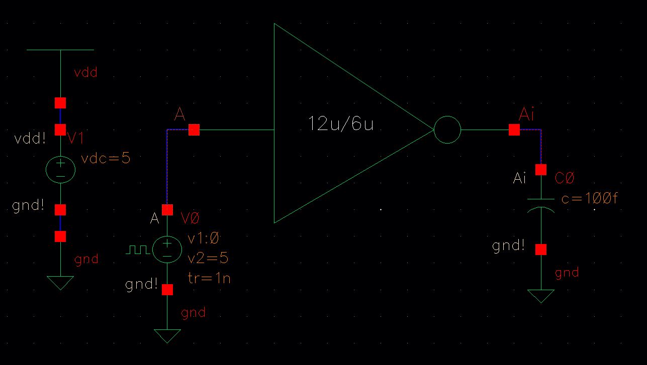
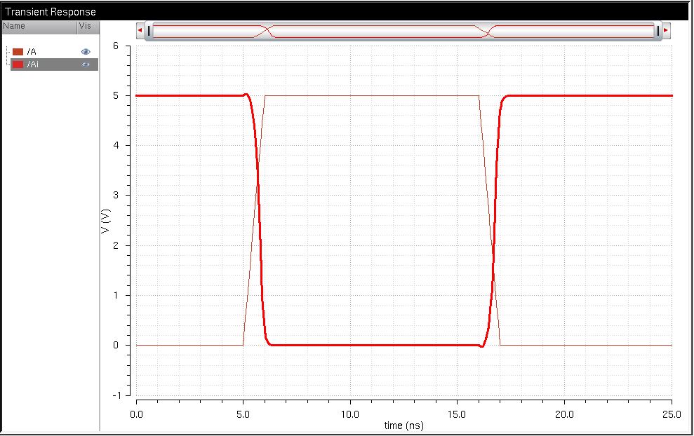
On
the 100 fF capacitor load, the output voltage charges and discharges
nearly instantaneously as the input voltage changes from high to low
and vice versa. 1 pF 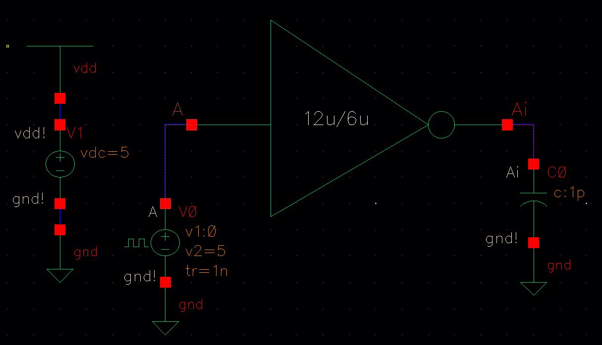
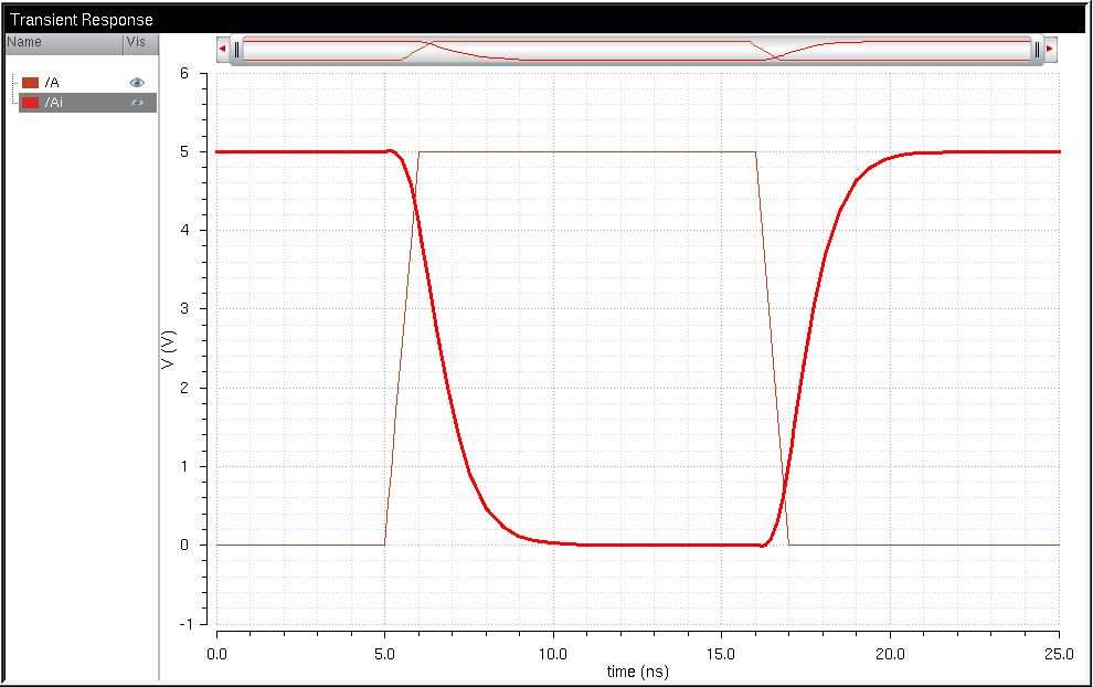
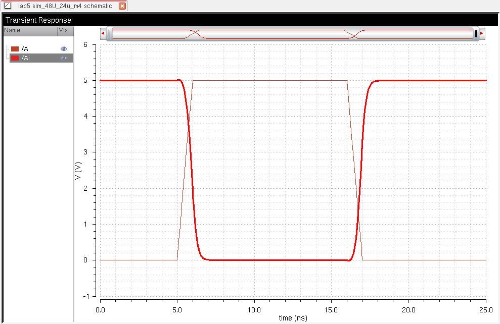
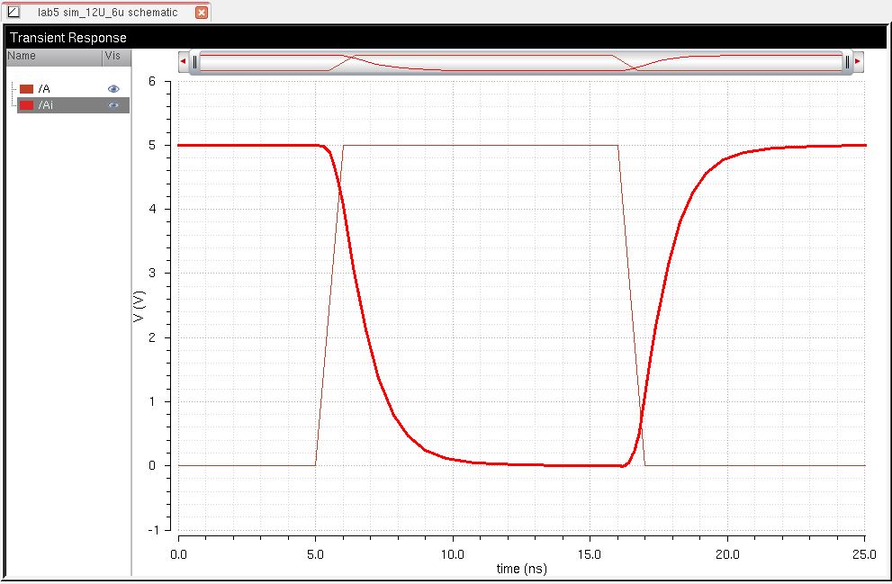
On the 1 pF load, there is a little more delay in the output voltage as the input switches. 10 pF 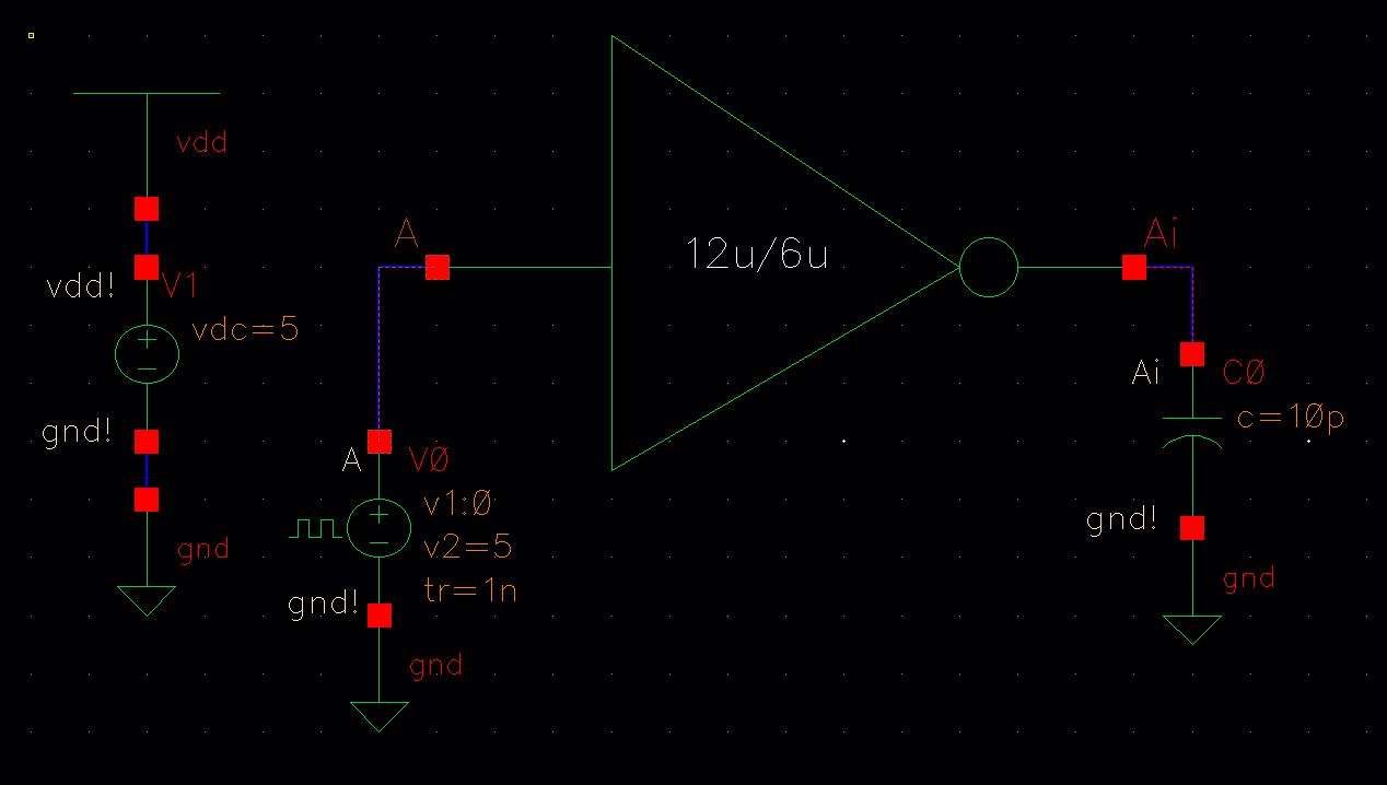
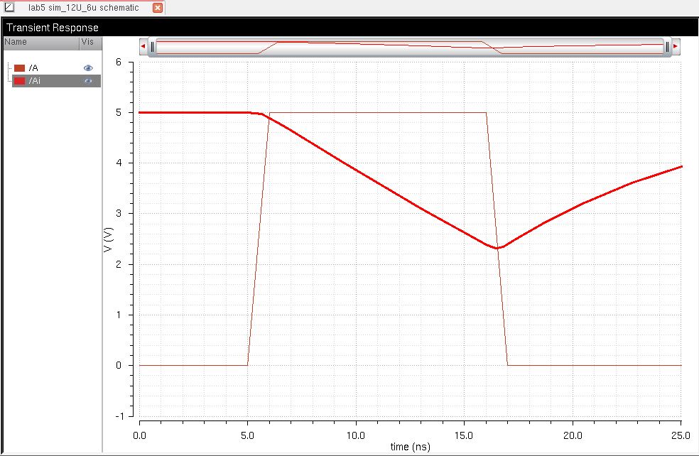
At
10 pF, the changes become much more noticeable, the charging and
discharging of the output voltage becomes heavily delayed, as it is not
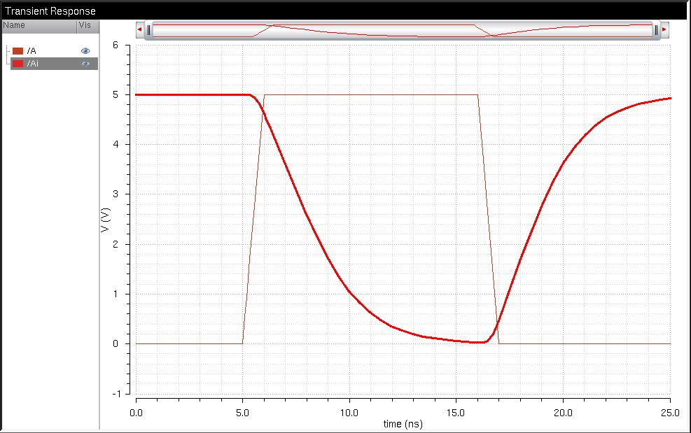
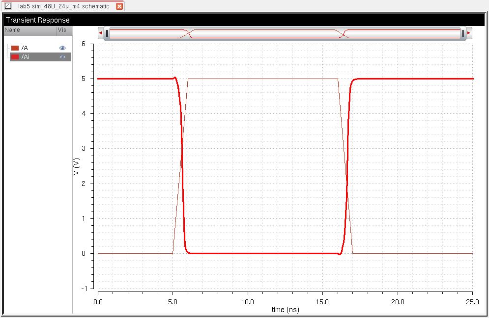
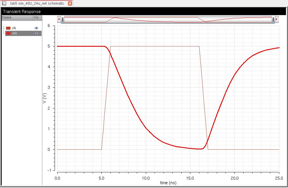
even able to reach minimum voltage before having to charge again. 100 pF 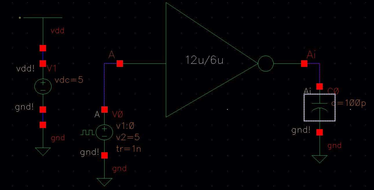
At 100 pF, the output voltage is nearly steady. There is mininimal change in the output voltage between charge and discharge.
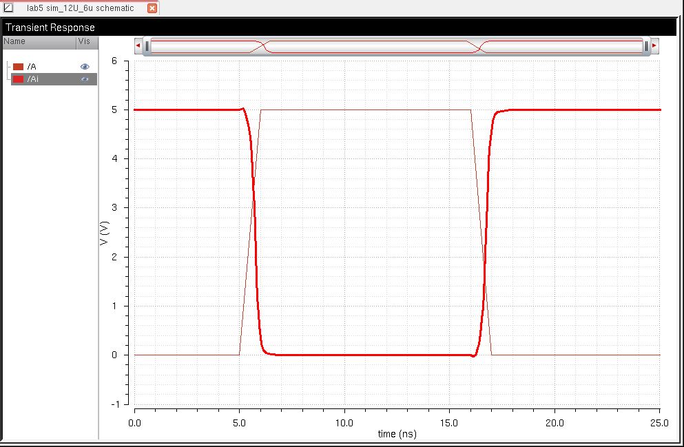
------------------------------------------------------------Load Schematic Simulation Comments 100 fF 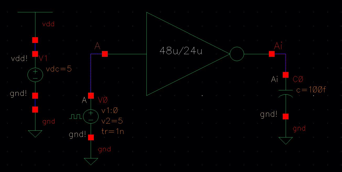
On 100 fF, charge and discharge is nearly instantaneous on output voltage with respect to input voltage. 1 pF 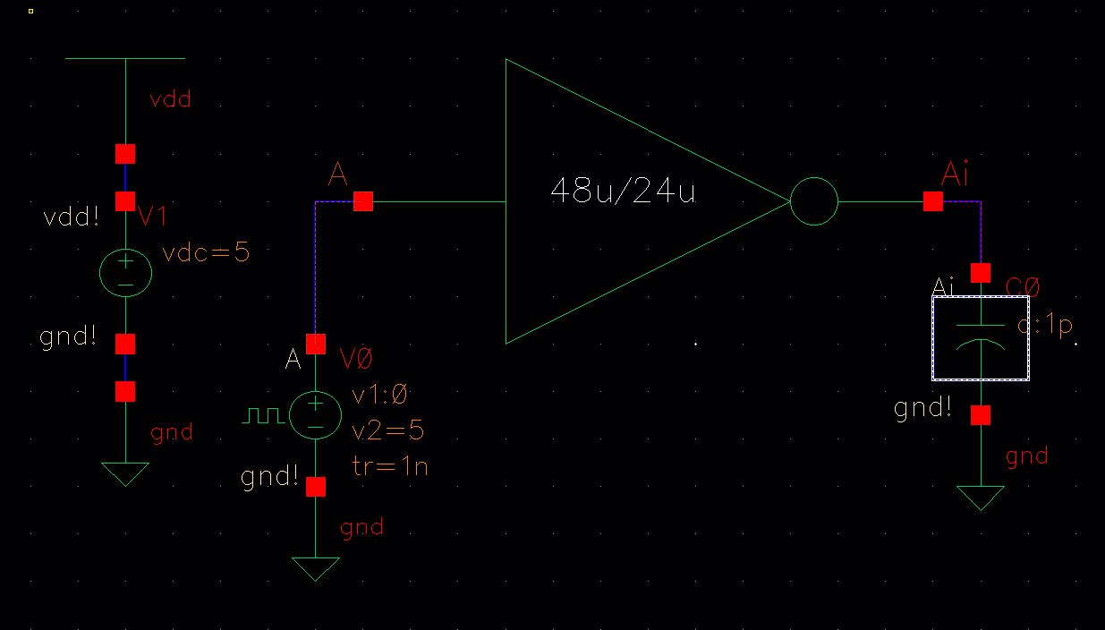
On 1 pF load, there is a much smaller delay increase for charging and discharging of output voltage compared to 12u/6u inverter. 10 pF 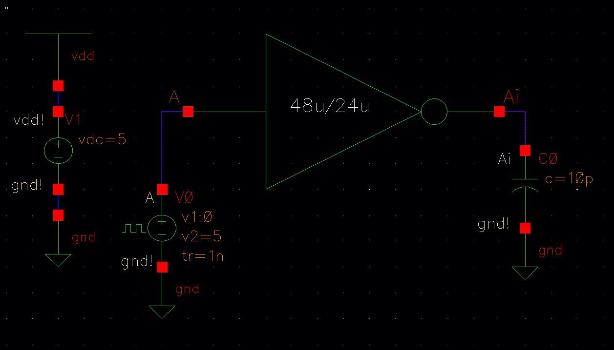
At 10 pF, the delay is larger between rise and fall, but minimum voltage is still reached. 100 pF 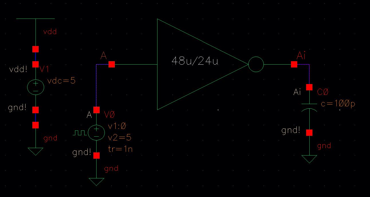
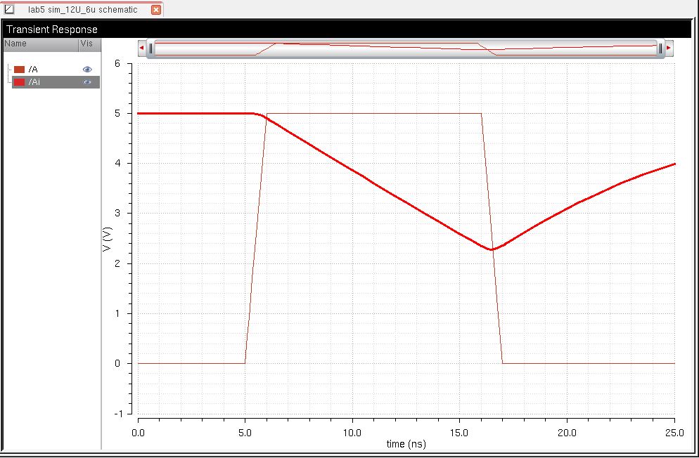
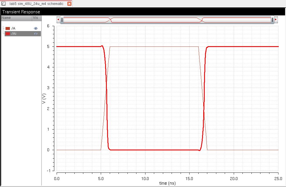
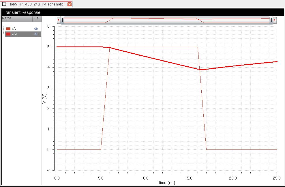
At
100 pF, the output voltage is nearly steady, but there is a larger
change from the maximum voltage compared to the 12u/6u inverter.
Load Schematic Simulations Comments 100 fF 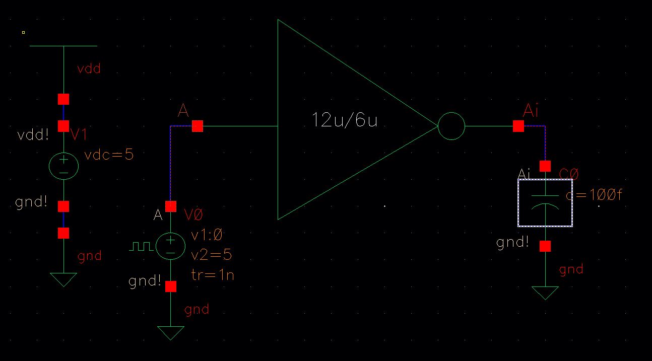
UltraSim
results show a near instantaneous change between high and low at the
output voltage as the input voltage changes at 100 fF load. 1 pF 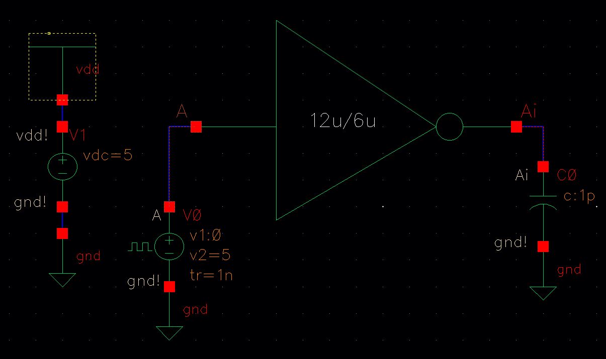
UltraSim results show a slight delay between high and low at the output voltage, similar to Spectre simulation. 10 pF 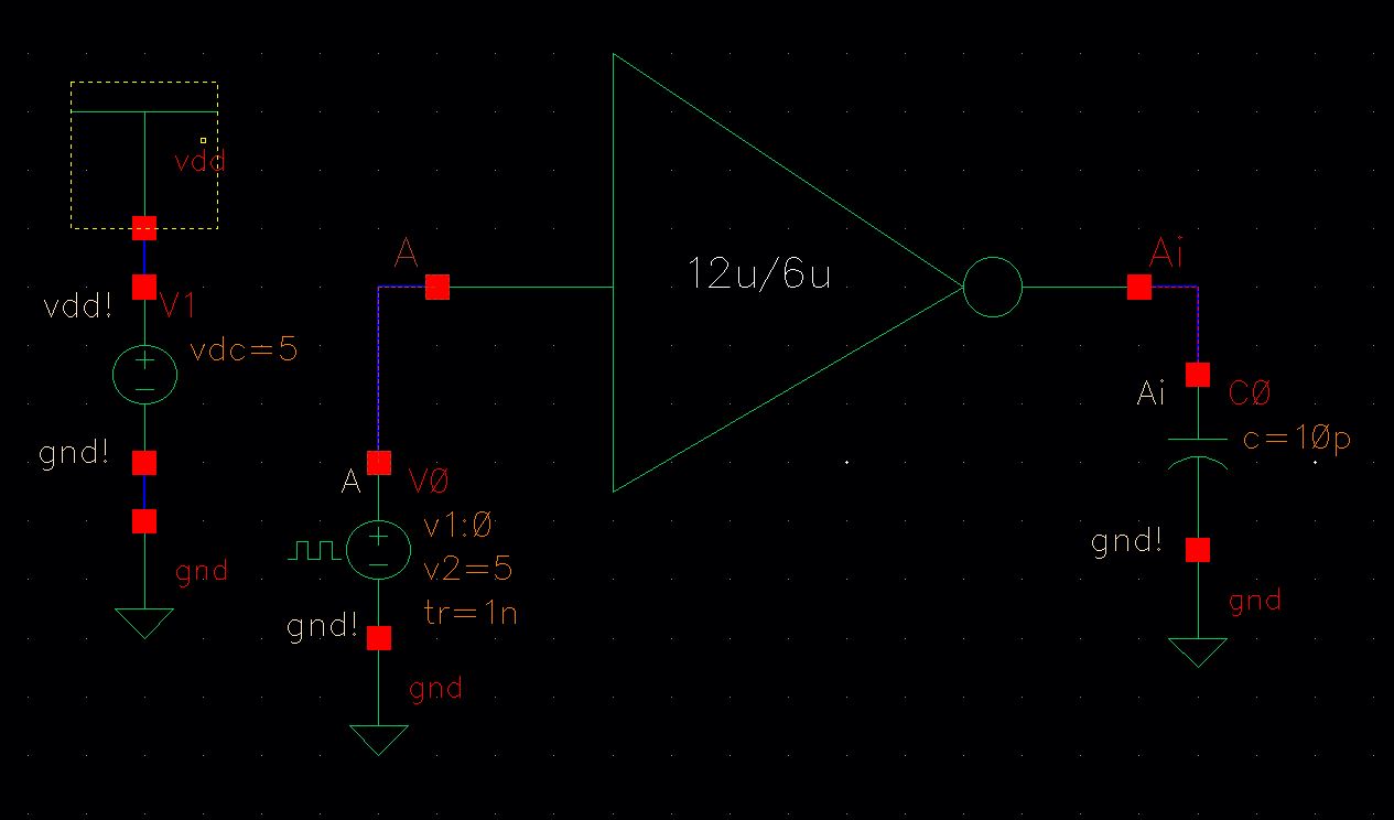
At 10 pF, minimum voltage is not reached at discharge, again, similar to Spectre sim. 100 pF 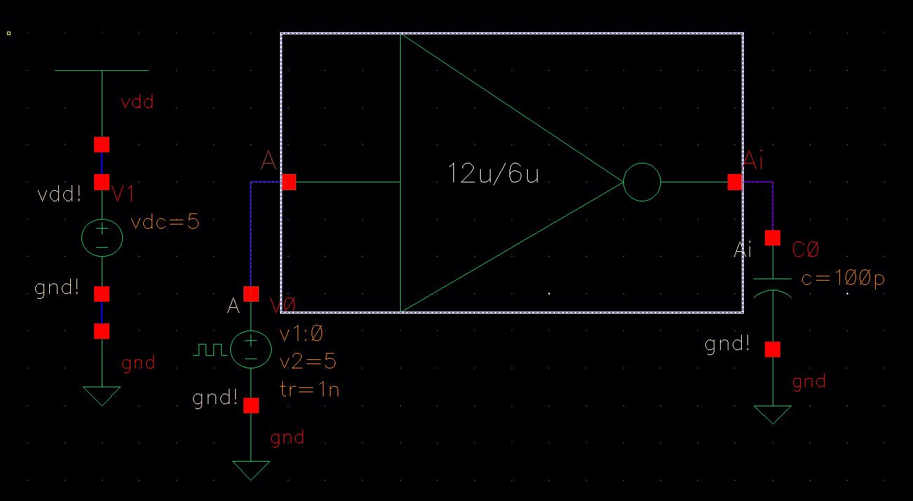
Output voltage is nearly steady at 100 pF, it nearly resembles a DC voltage reading with this load.
Load Schematic Simulation Comments 100 fF 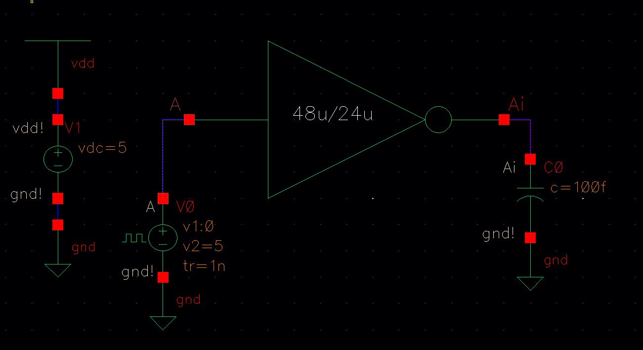
At 100 fF, the discharge is nearly instantaneous across high and low, similar to Spectre Sim. 1 pF 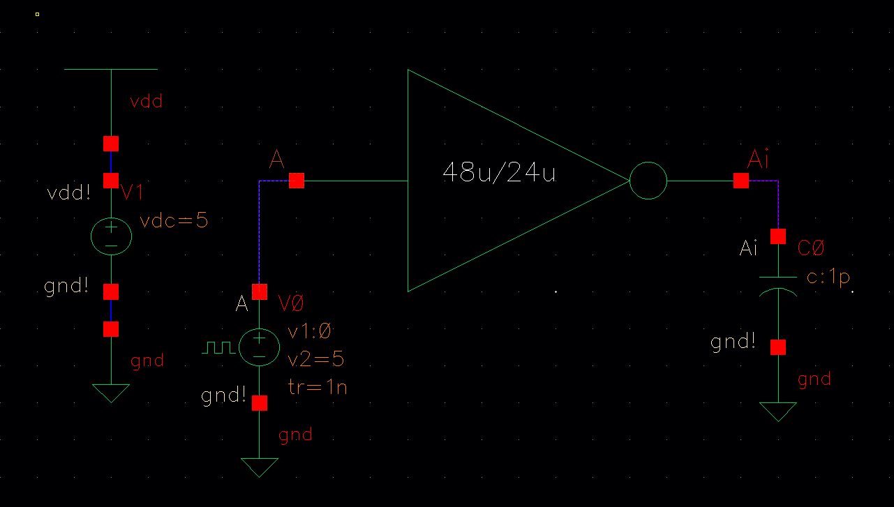
At
1 pF, there is a small delay at rise and fall times for output voltage,
but it is still nearly instantaneous, similar to Spectre Sim. 10 pF 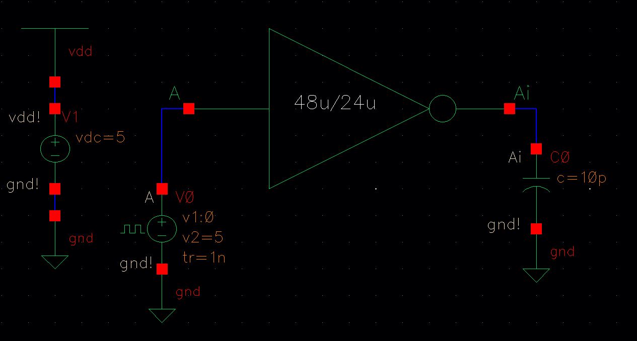
There is more of a delay at rise and fall times for output voltage at 10 pF, but minimum voltage is still reached. 100 pF 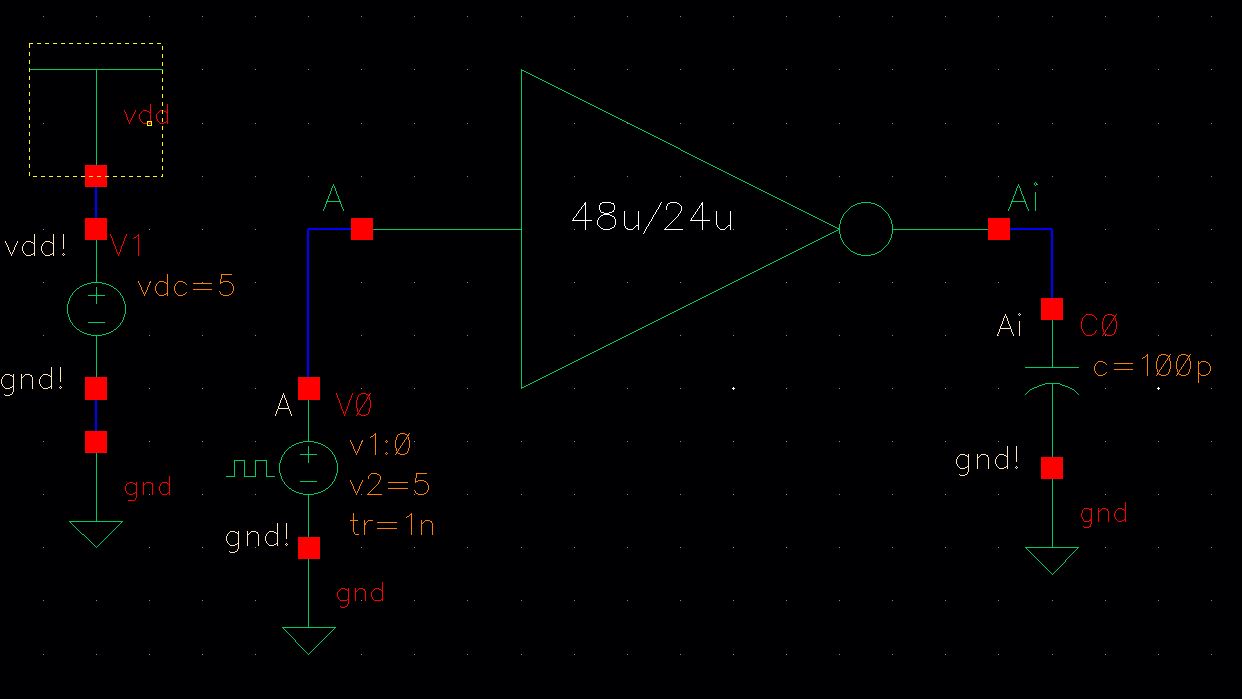
The
output voltage almost resembles a DC reading, but there is more of a
change between max voltage and the discharge voltage before the
capacitor recharges again.