Project - ECE 421L
Design a serial-to-parallel converter that takes serial input data and an associated clock signal and generates an 8-bit output (parallel) word and clock.
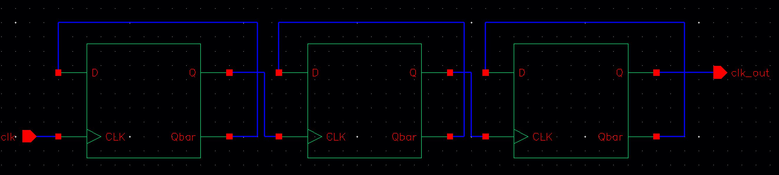
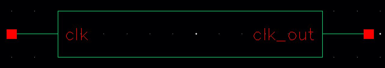
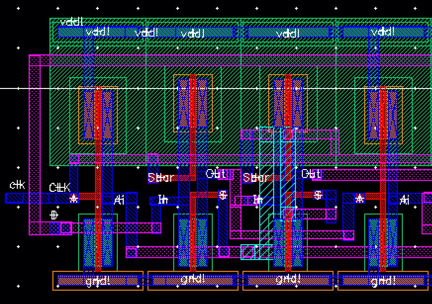
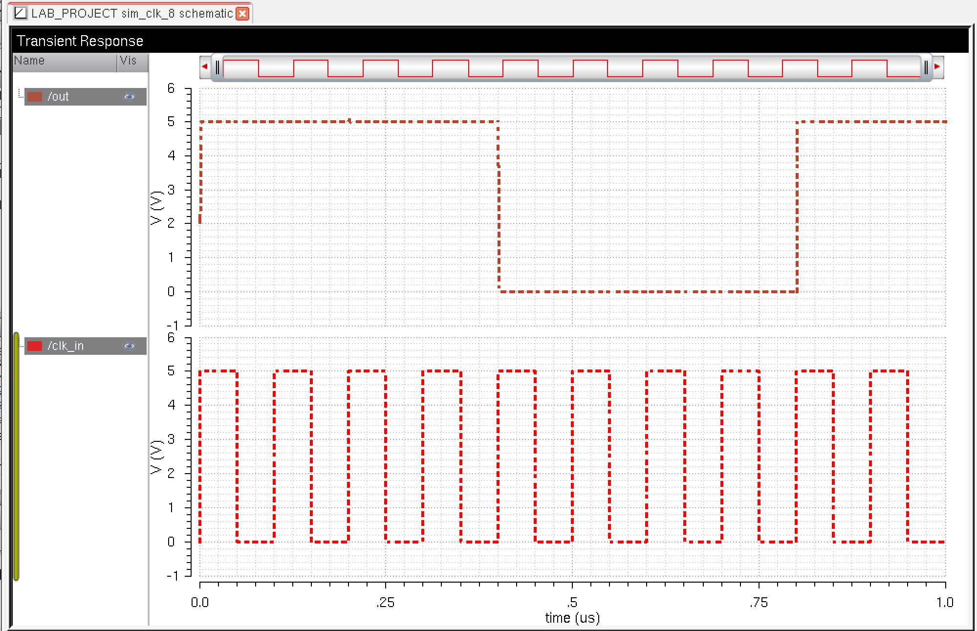
I created a symbol to simulate Clock_out which would act as clk/8. I used three D Flip Flops to simualte clock/2^N with N as the number of D Flip Flops.
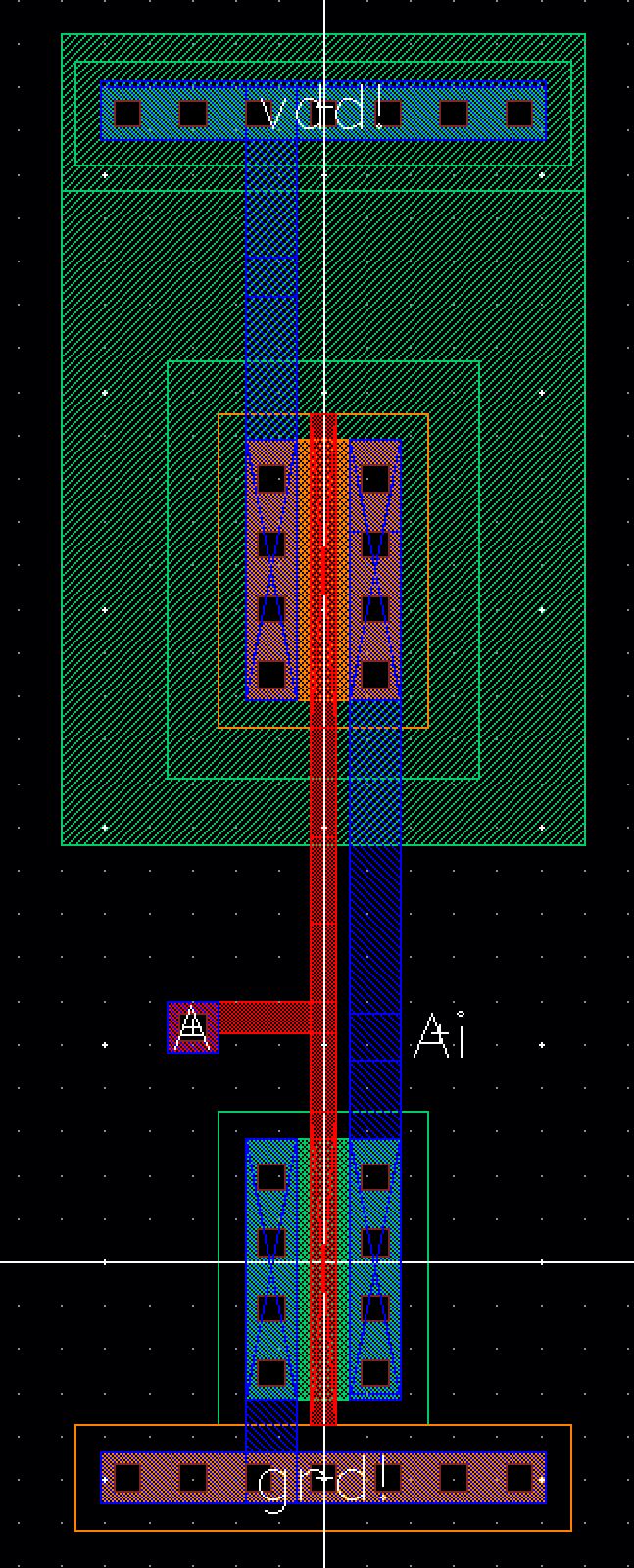
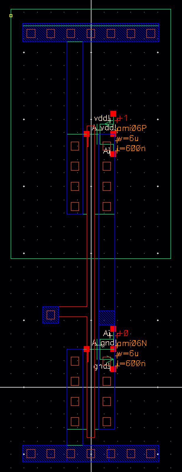
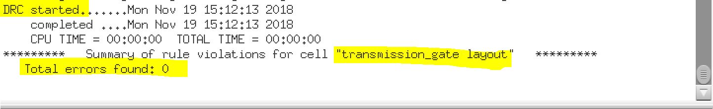
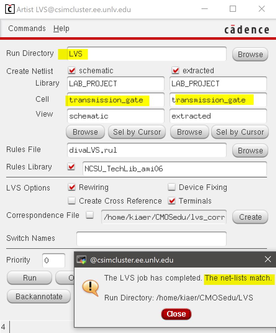
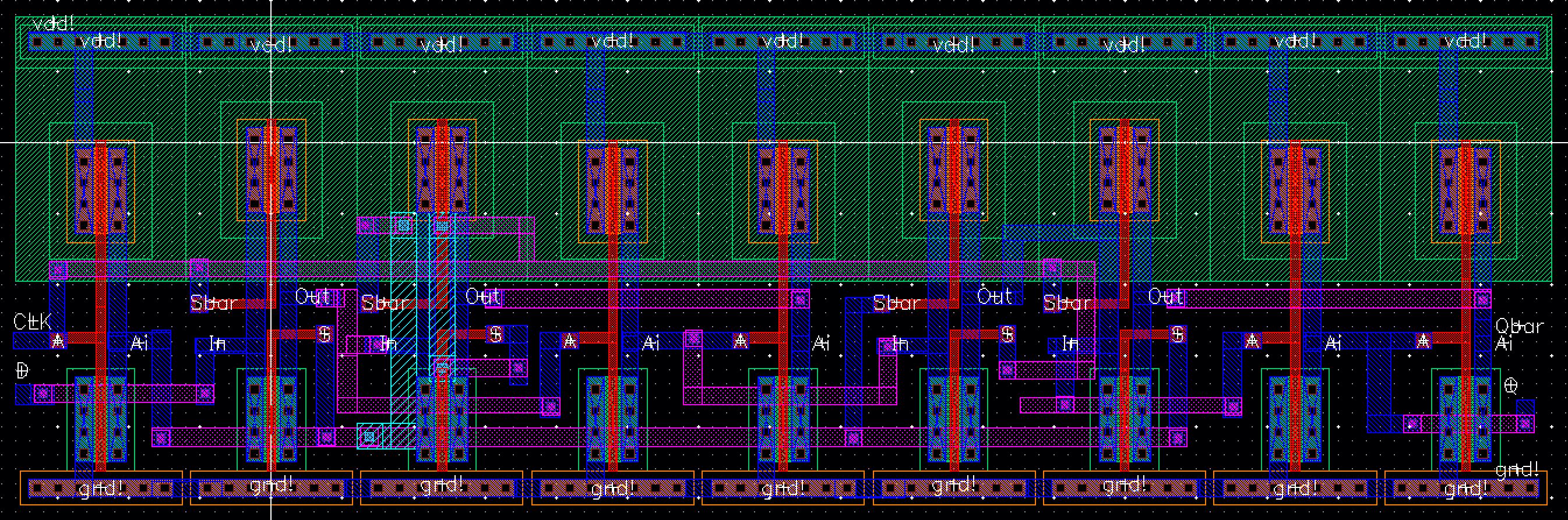
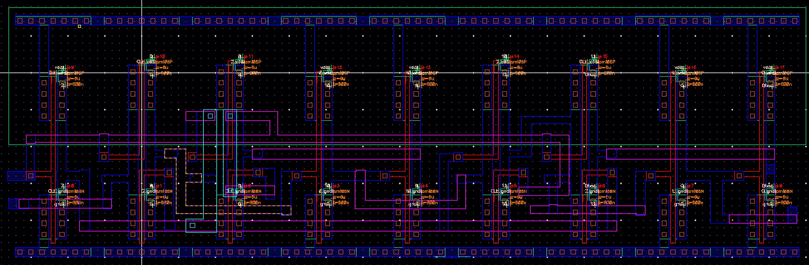
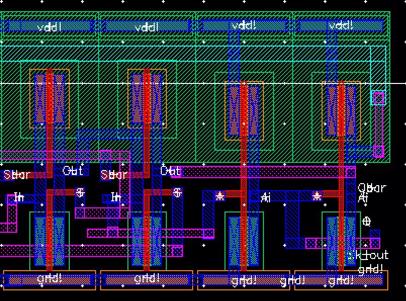
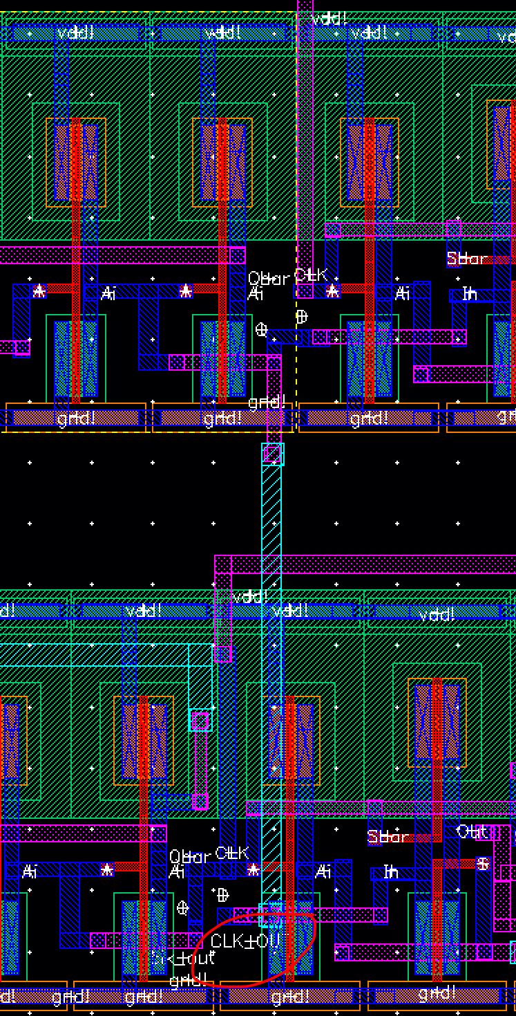
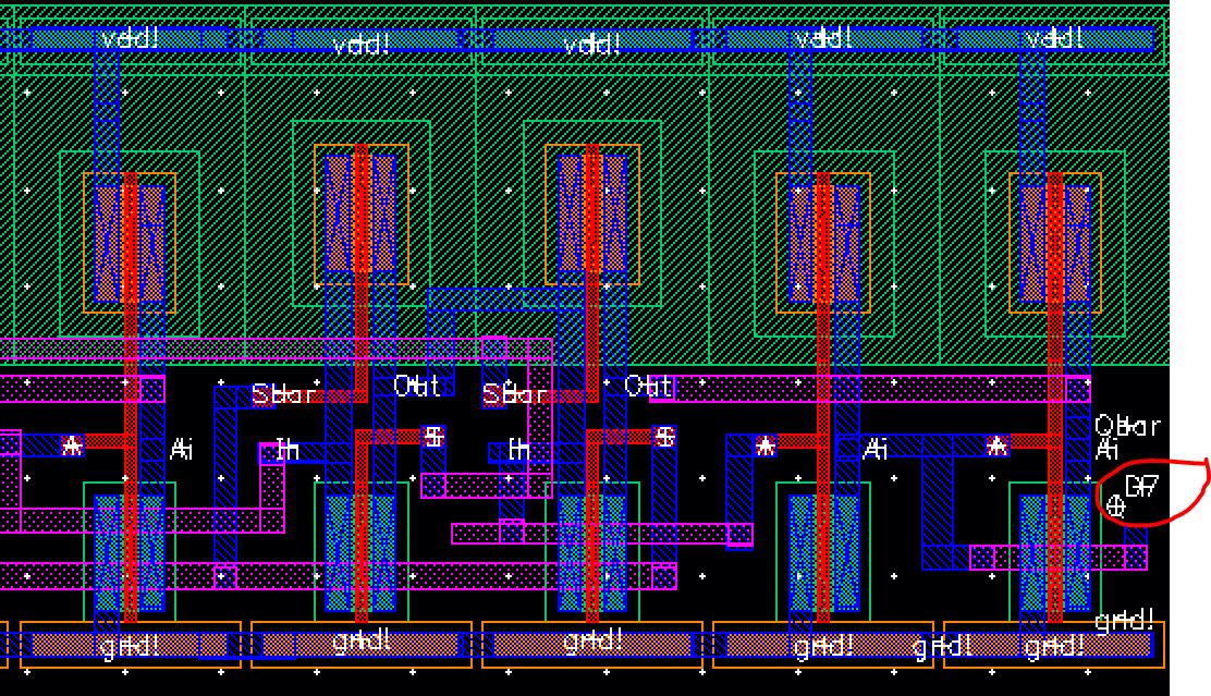
Layout:
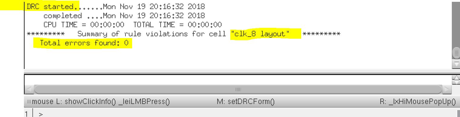
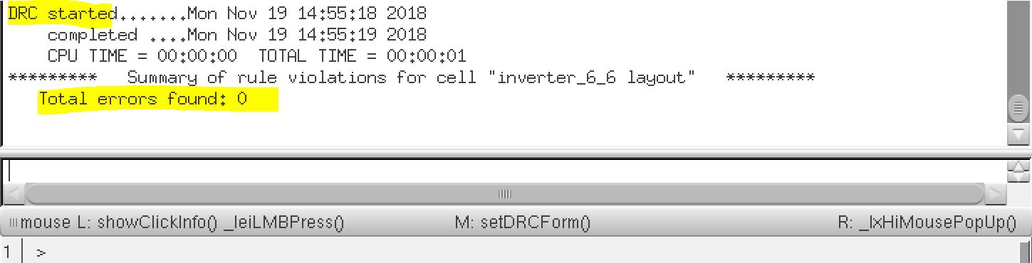
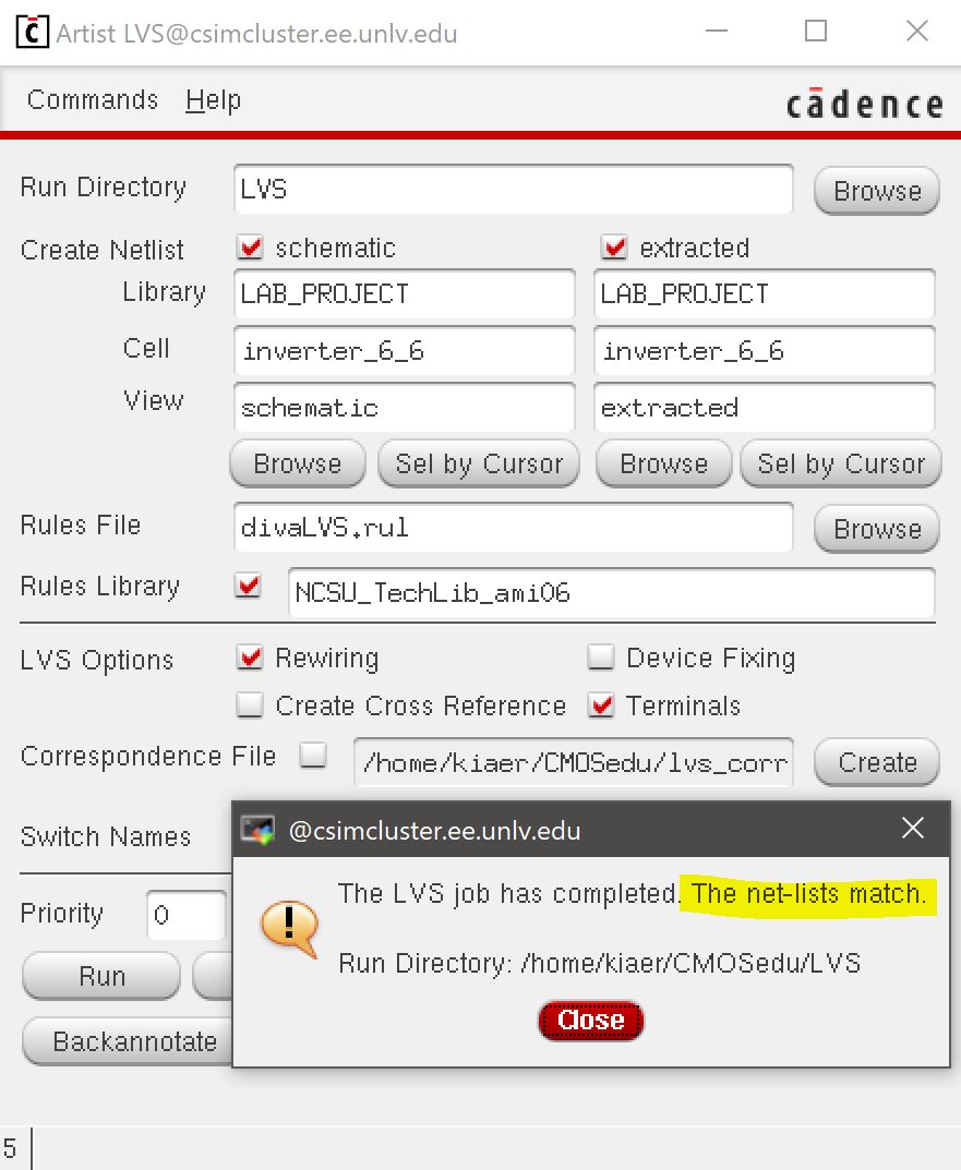
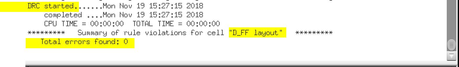
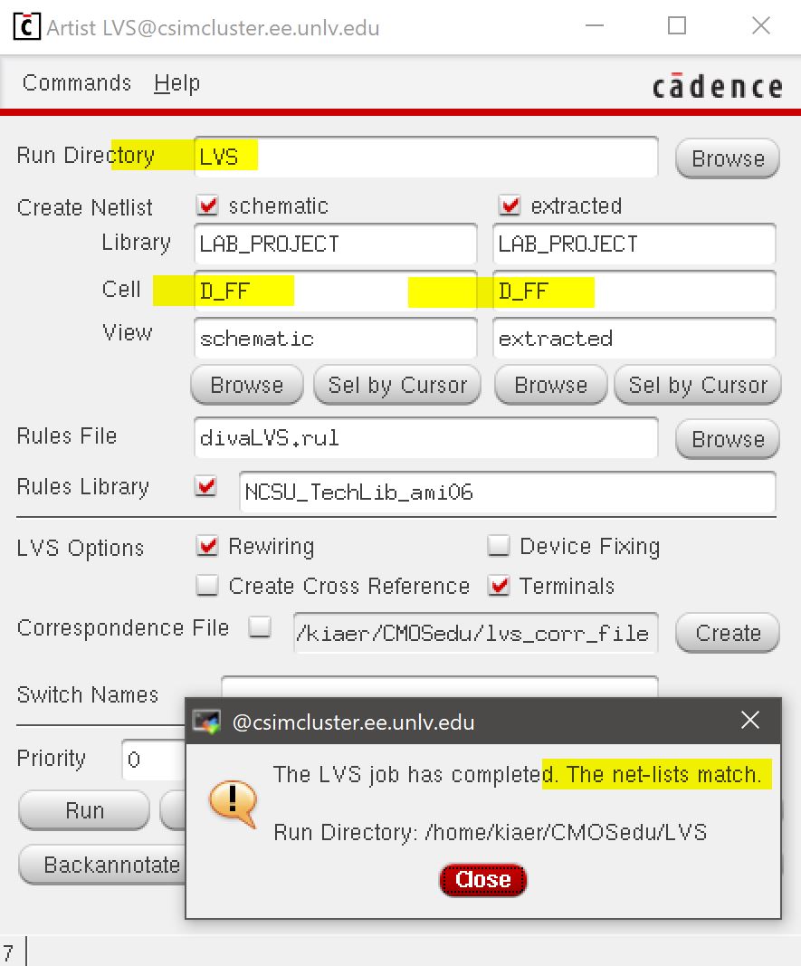
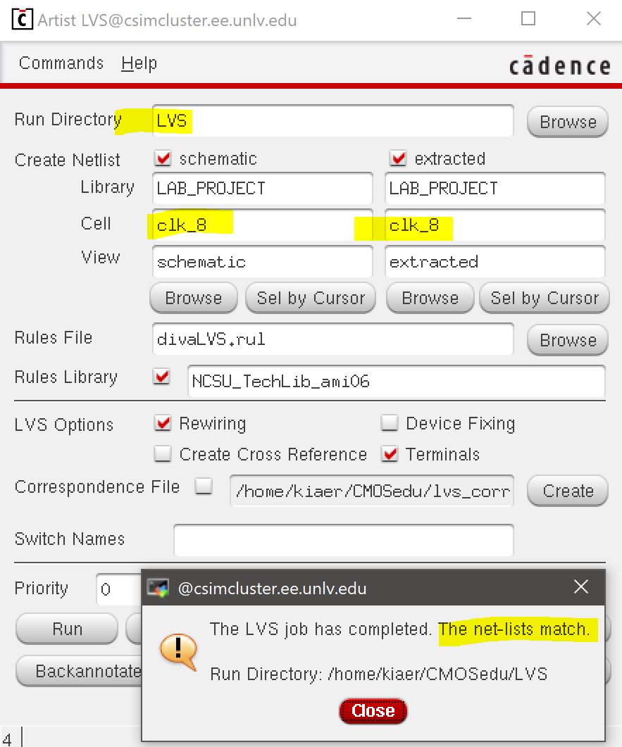
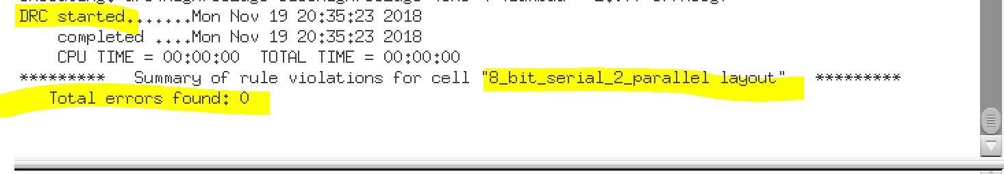
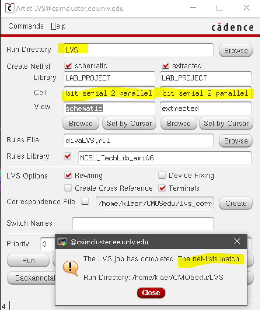
LVS
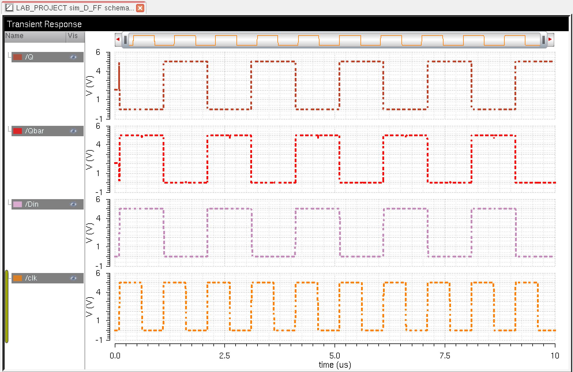
CLOCK/8 OUTPUT SIMULATION:
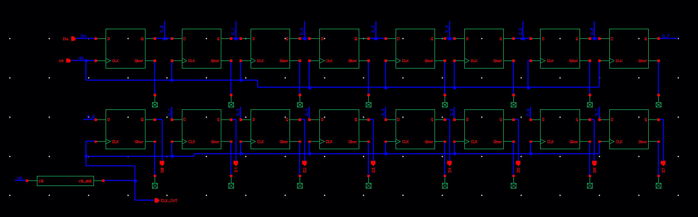
8-bit Serial-to-Parallel Converter:
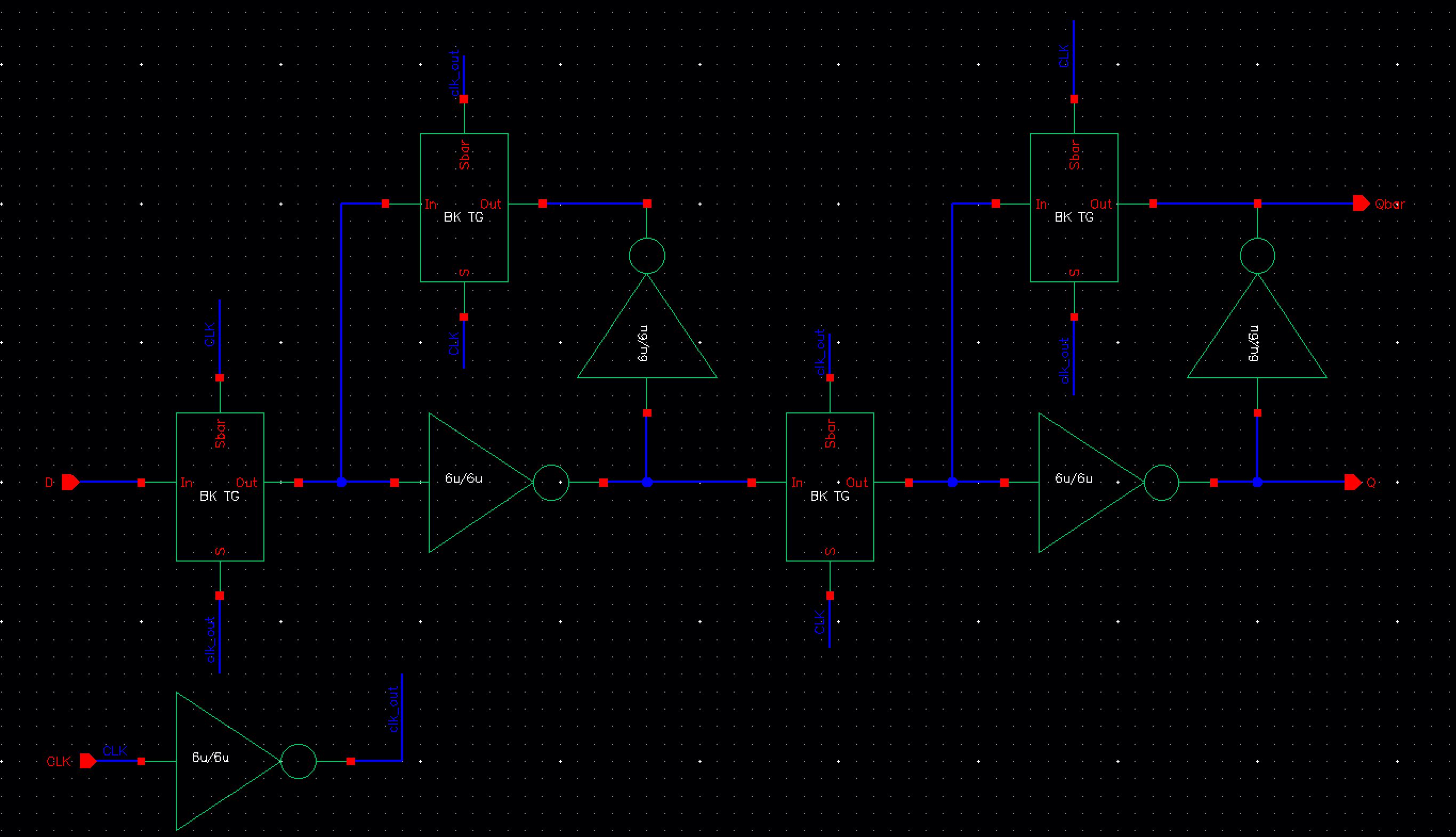
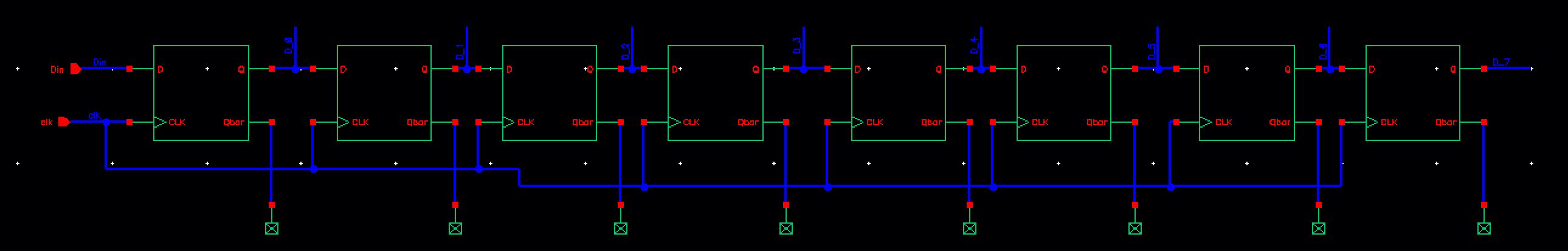
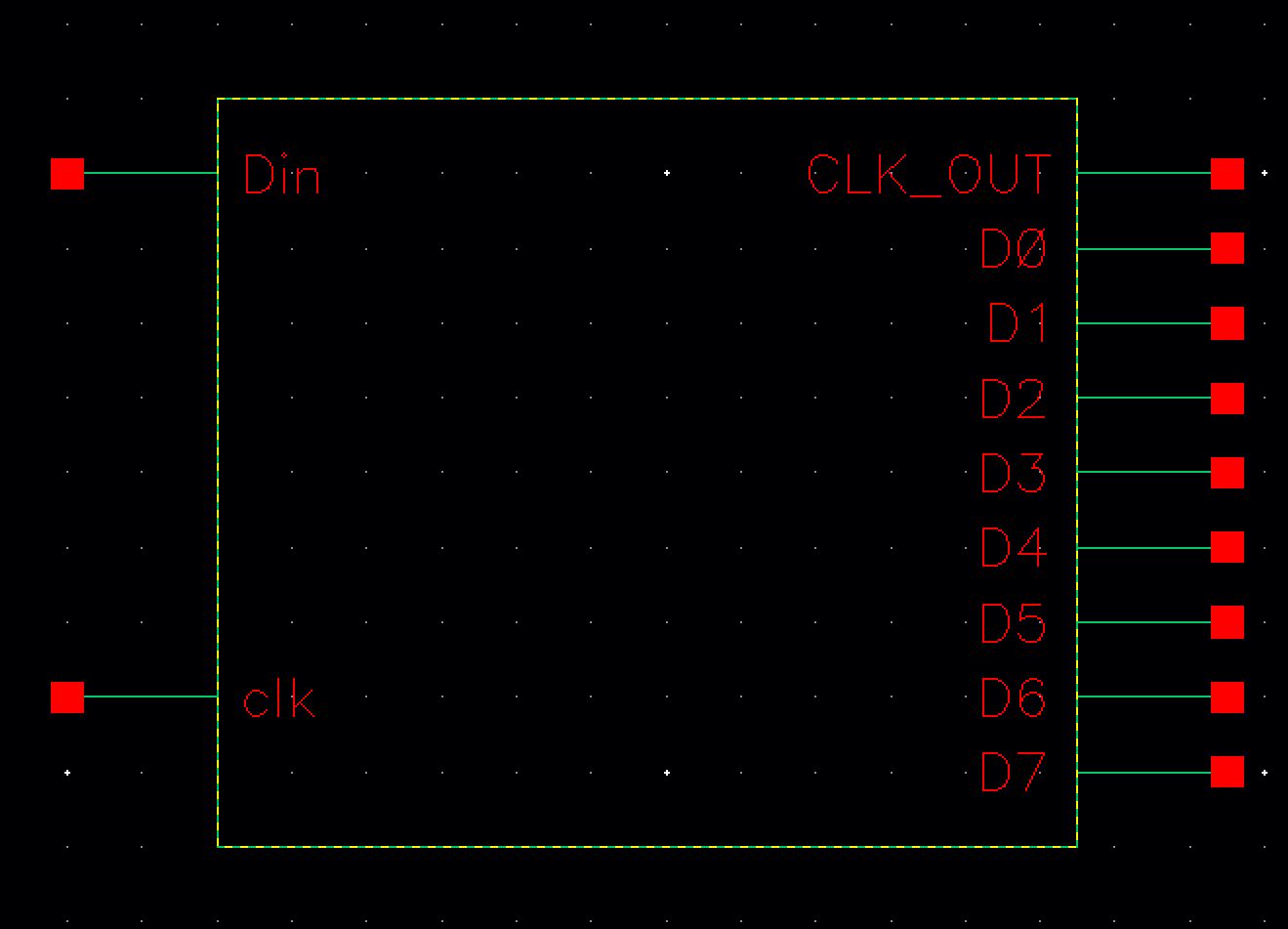
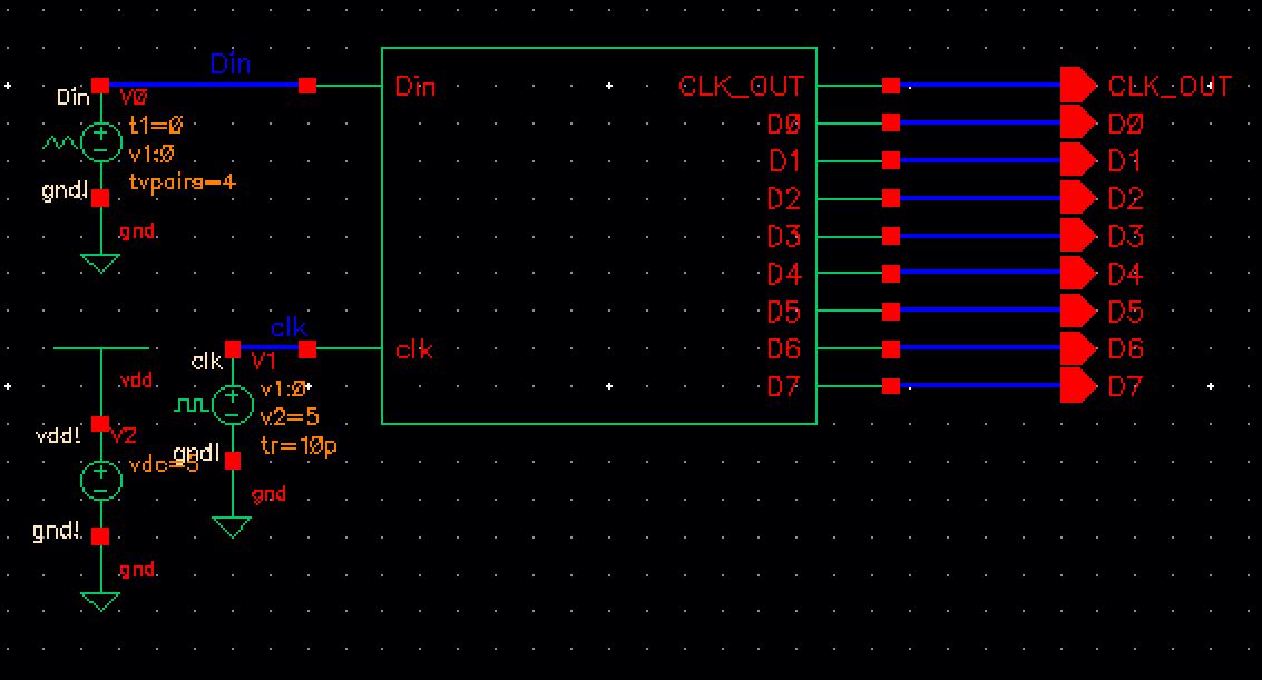
Here is the final schematic used for the 8-bit Serial-to-Parallel Converter. This schematic uses two main registers the Shift Register and the Hold Register shown below. The Shift Register uses the normal clock input while the Hold Register uses clock_out which in this case is clock/8. The input is connected to the CLK_OUT symbol above to implementthe effects of clock_out. Lastly, I created a symbol that has two inputs (Din and clk) and nine outputs (D0-D7 and CLK_OUT).
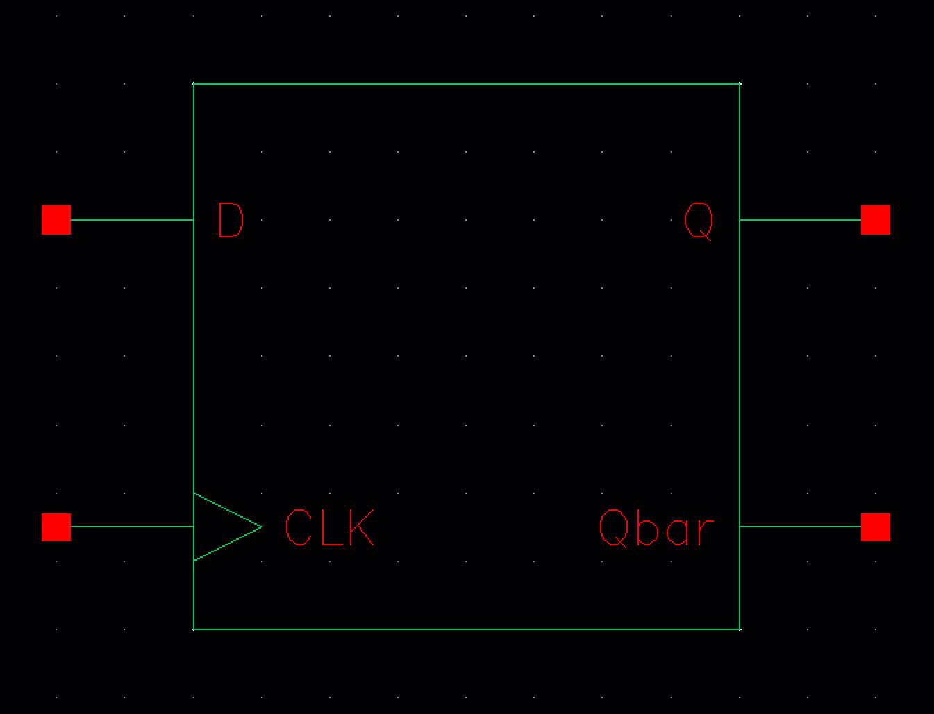
Shift Register:
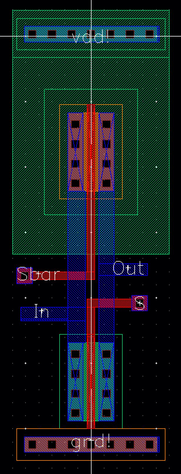
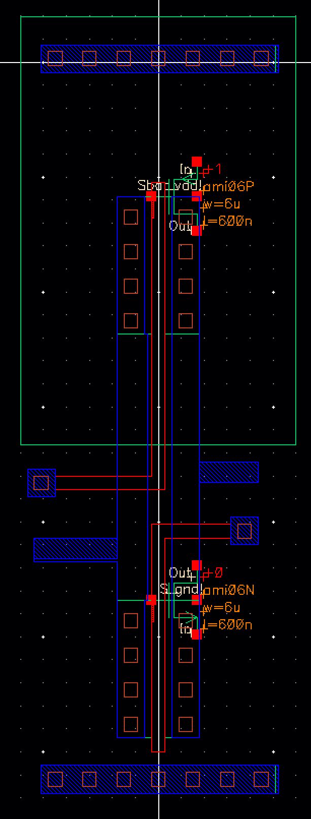
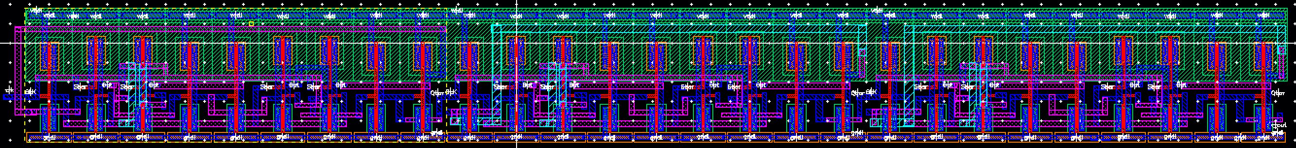
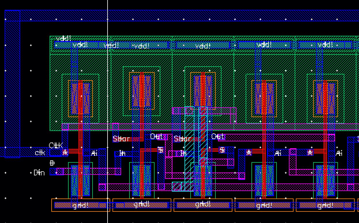
Full Shift Register Layout (click to zoom):

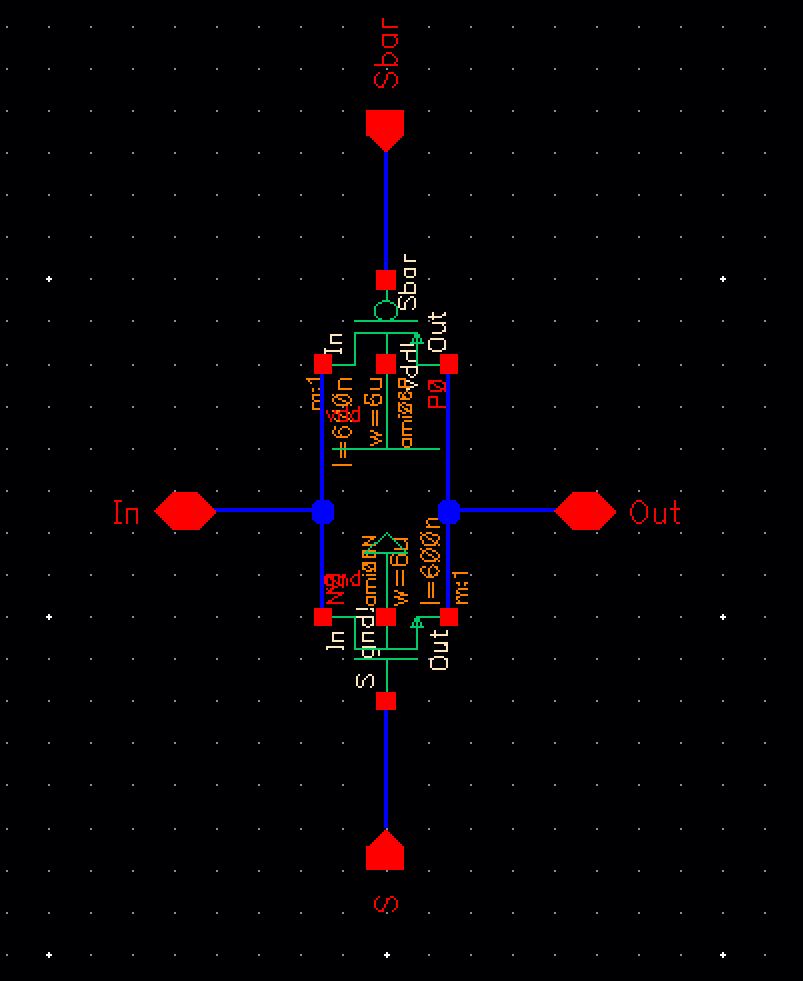
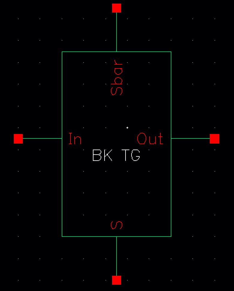
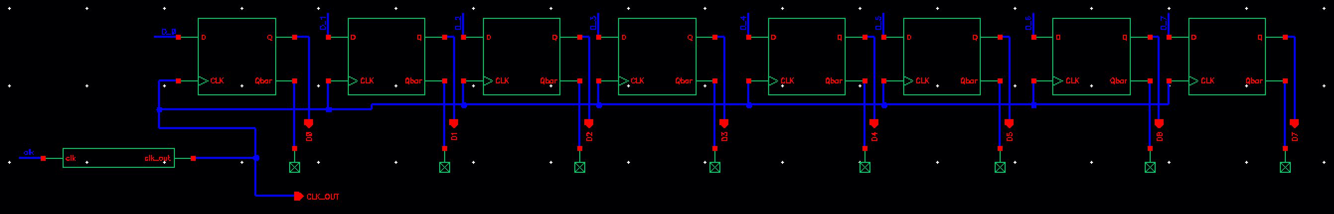
Hold Register:
Schematic:

Full Schematic:
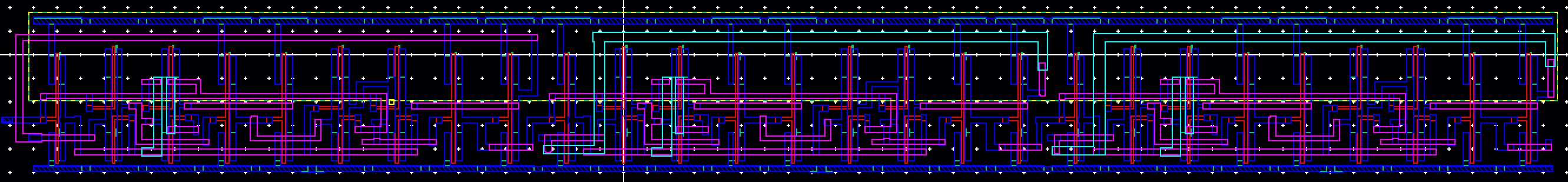
Full Layout of 8-bit Serial-to-Parallel Converter: (click to zoom)

LVS
Simulations:
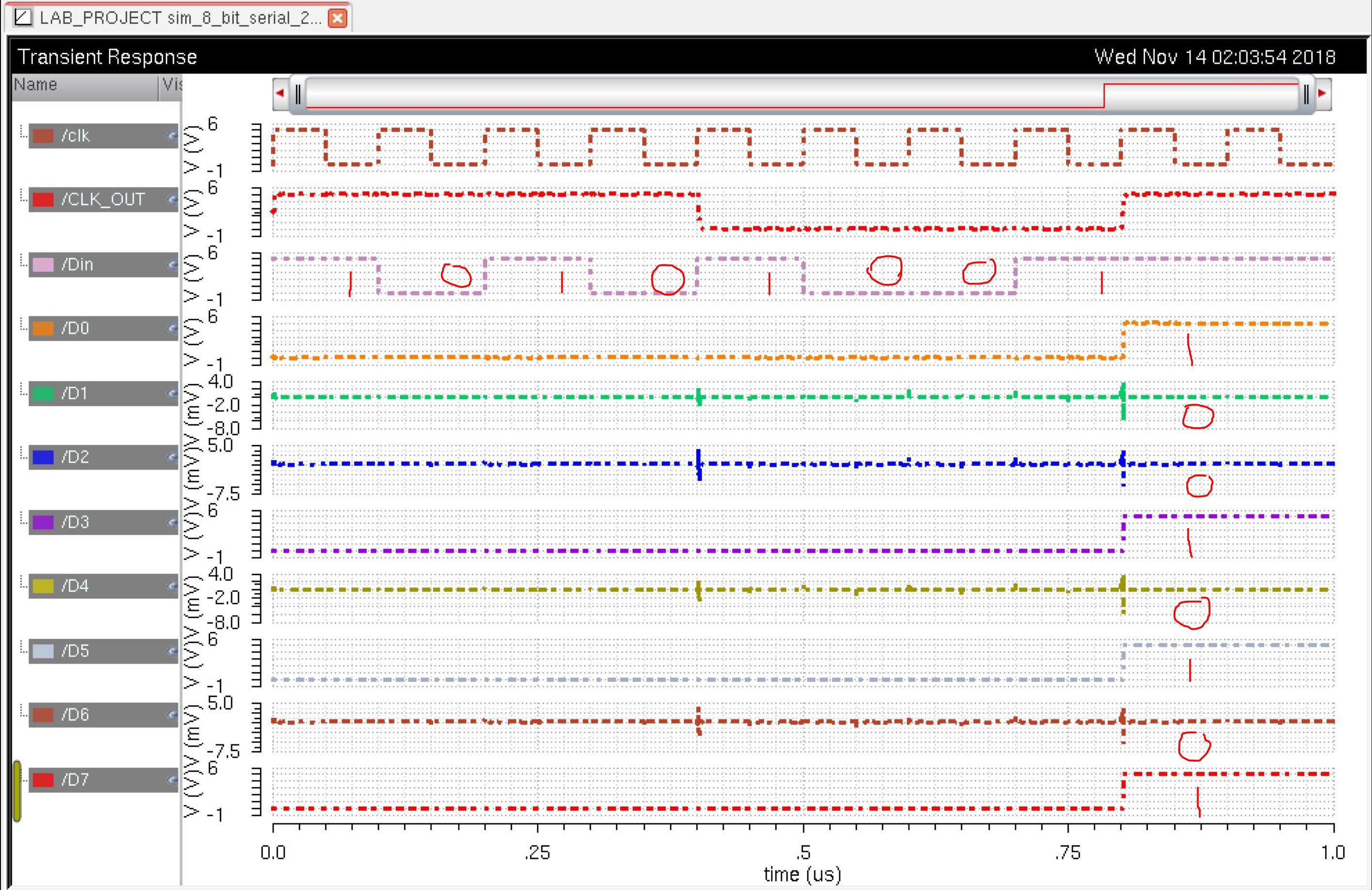
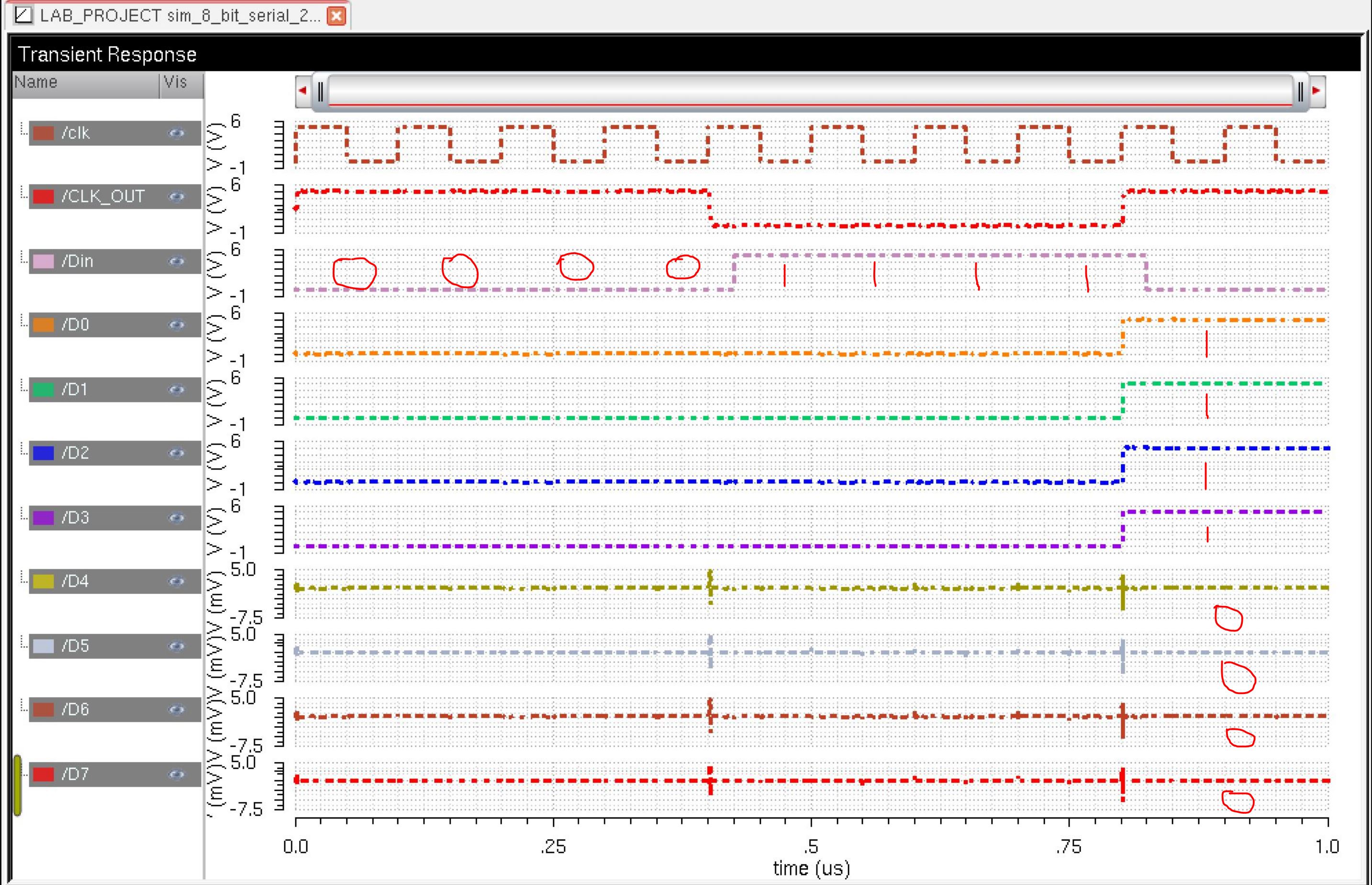
Here is the output waveform of the above schematic above. For this simulation the output I am aiming for is to get 11110000.
When looking at the waveform output D0-D7 the results are 11110000 at 0.8 us.
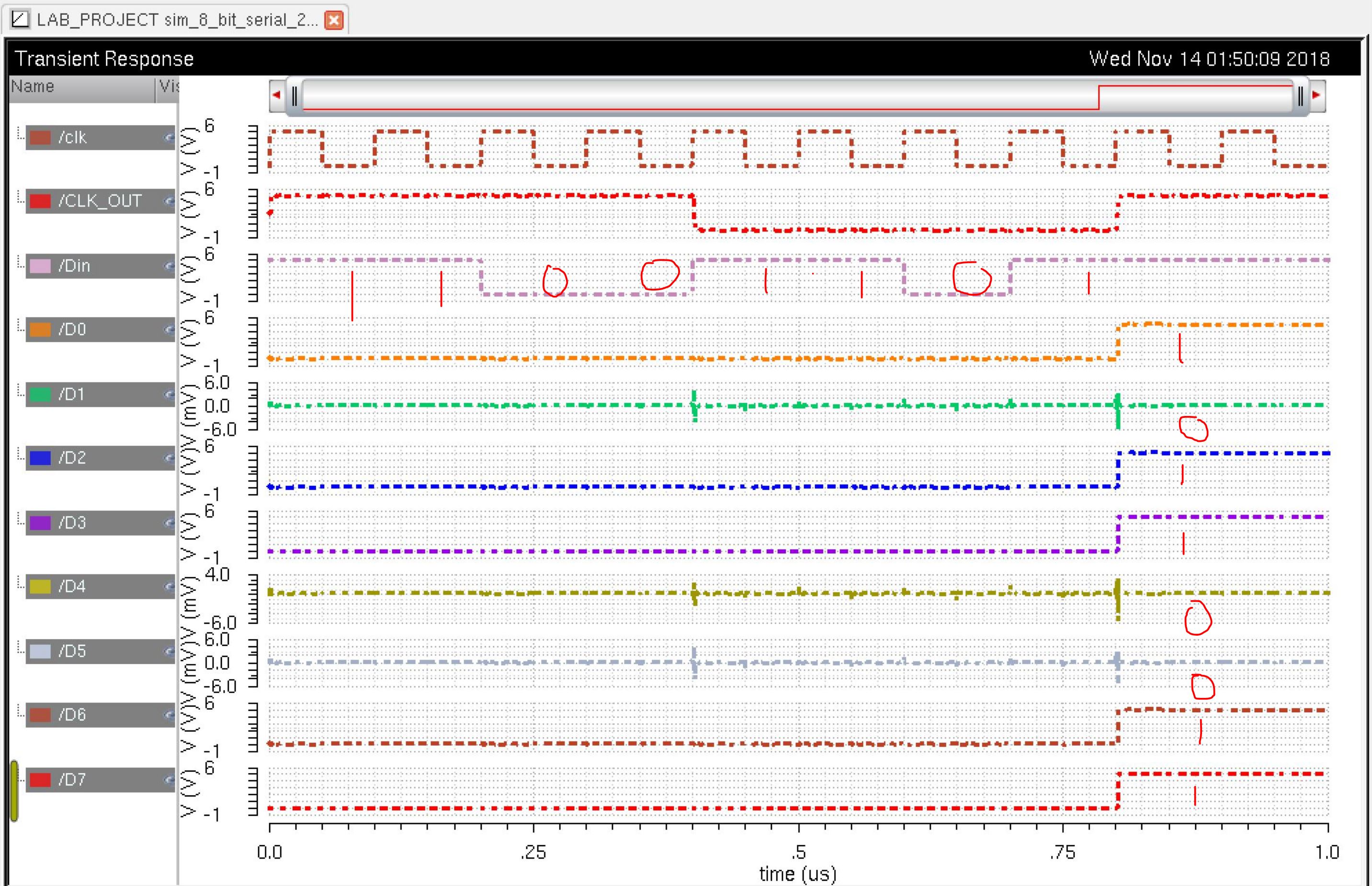
Here is a second simulation using a serial input for Din to get an output of 10110011. When creating the input Din is inputted as 11001101.
When looking at the output from D0-D7 the output is as expected at 0.8us 10110011.
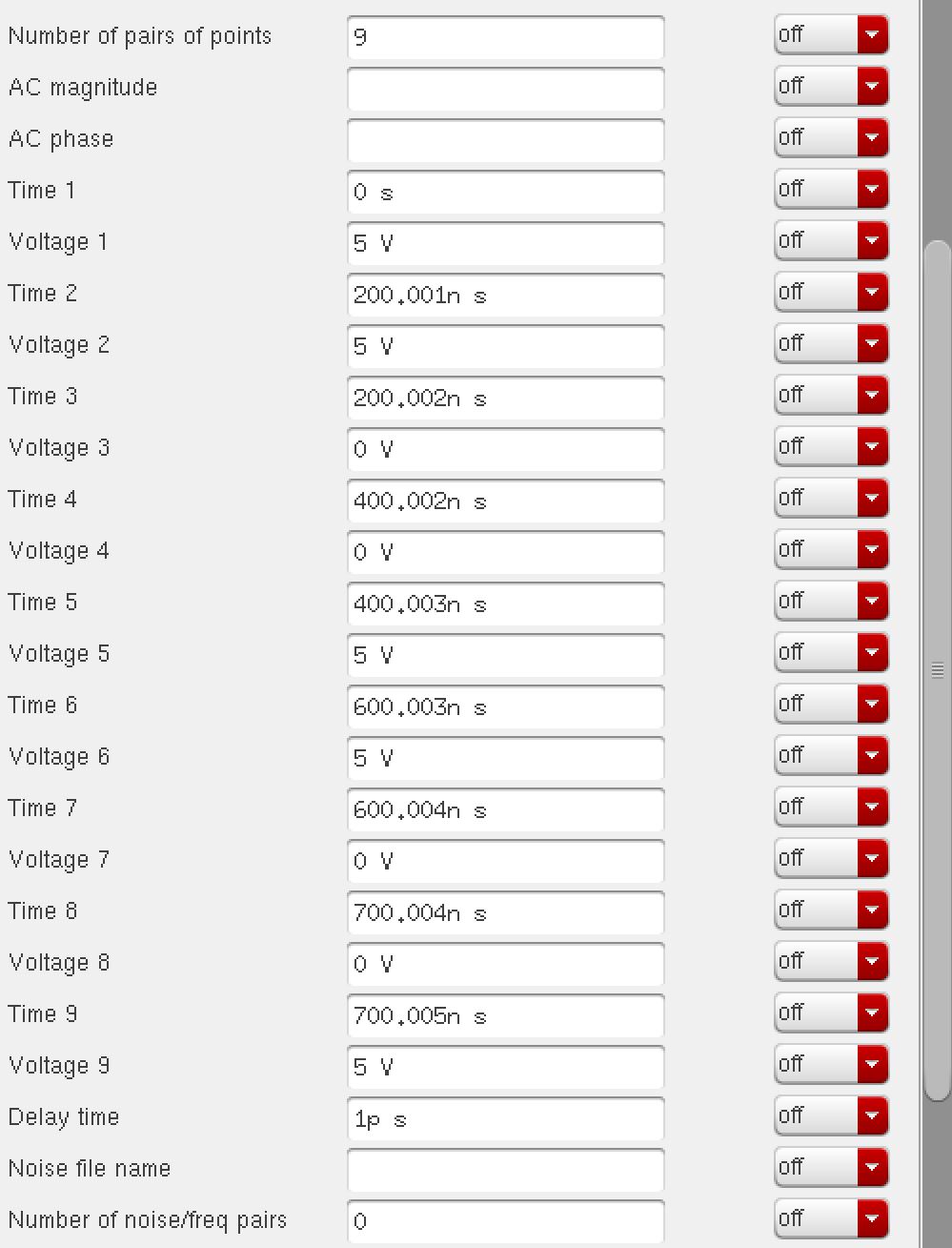
Here is a third simulation using a serial input for Din to get an output of 10010101. When creating the input Din is inputted backwards as 10101001.
When looking at the output from D0-D7 the output is as expected at 0.8us 10010101.