Lab 7 - ECE 421L 

Brian Medrano Kiaer

kiaer@unlv.nevada.edu

November 6th 2018

Prelab: 

For the prelab we are required to go through Tutorial 5 which corresponds to creating a design, a layout, and a simulation of a ring oscillator. 

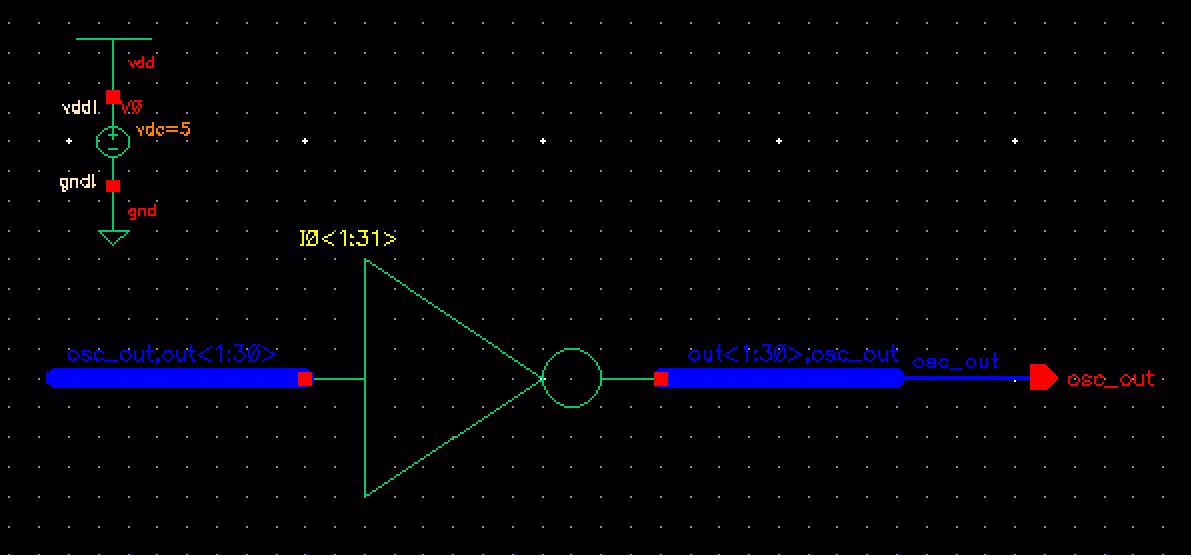
This is the schematic for the ring oscillator within Tutorial 5. Above the inverter symbol where it states "I0<1:31>" that is stating that this is a 31 stage ring oscillator. A wide wire is added to act as a bus for the multiple signals of the ring oscillator.

http://cmosedu.com/jbaker/courses/ee421L/f18/students/kiaer/lab7/snip1.JPG

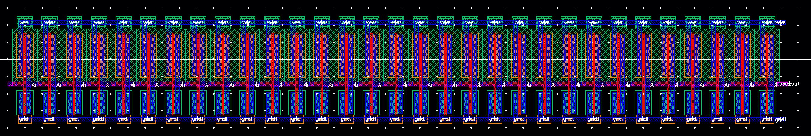
Then I created the layout of the 31 stage ring oscillator. I first instantiated the layout used previously for one inverter and then created connections and copied that layout 30 more times to a matched layout to the schematic.

http://cmosedu.com/jbaker/courses/ee421L/f18/students/kiaer/lab7/snip3.JPG

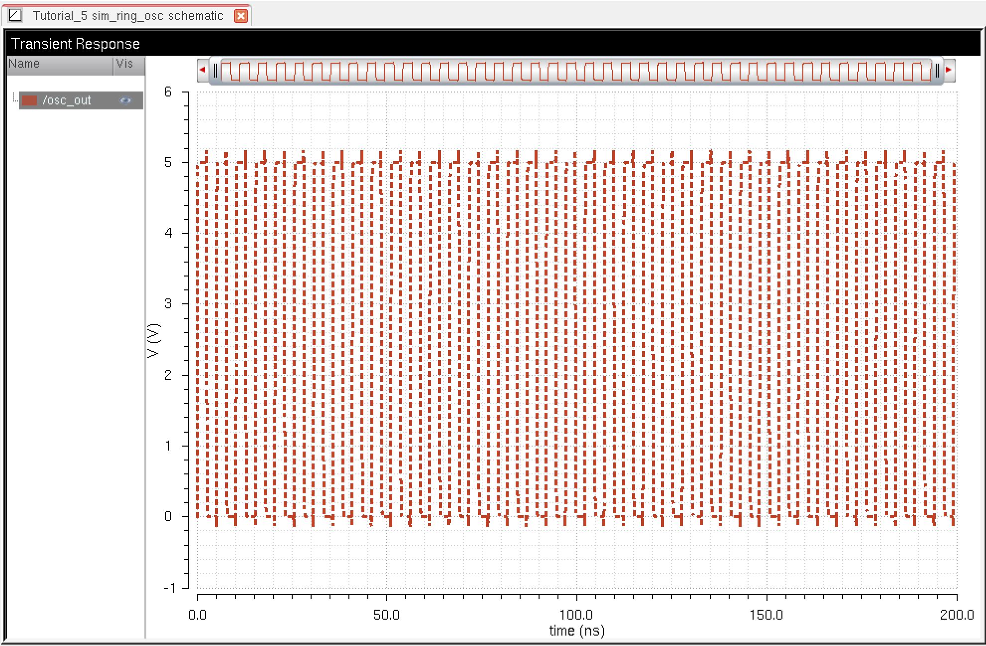
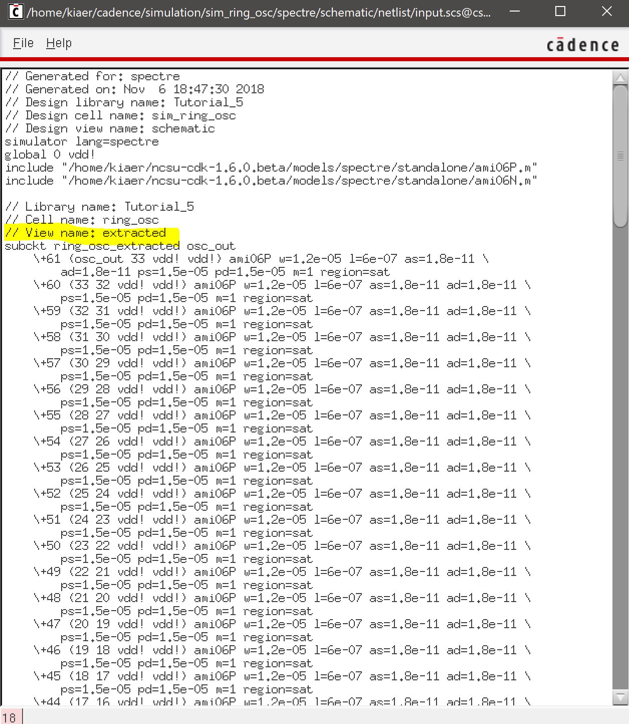
Next, I performed a simulation on a cellview called "sim_ring_osc" and used the extracted view to ensure that the outcome was the same as 31 inverters in series.

http://cmosedu.com/jbaker/courses/ee421L/f18/students/kiaer/lab7/snip2.JPG

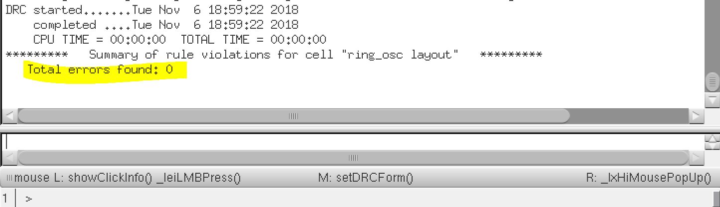
I  ensured that the layout passed the DRC verification.

http://cmosedu.com/jbaker/courses/ee421L/f18/students/kiaer/lab7/snip4.JPG

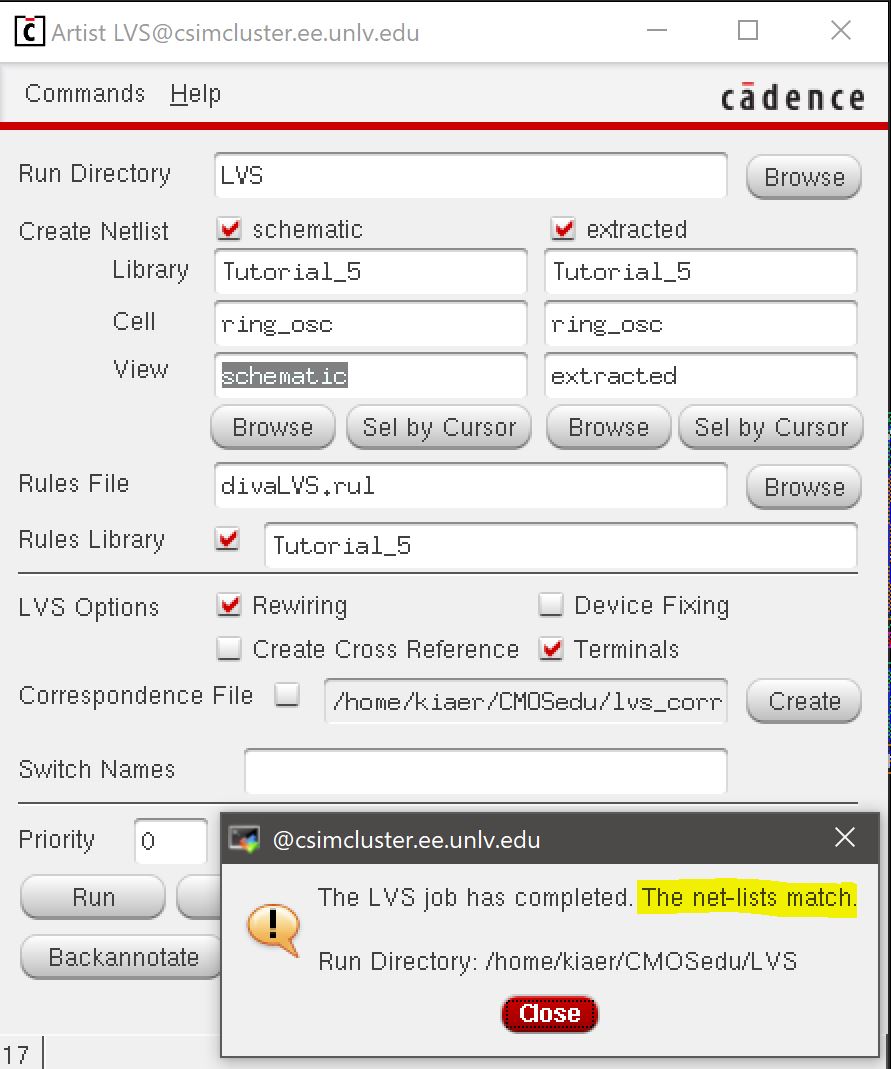
I also ensured that the layout, extracted view, and schematic passes the LVS verification.

http://cmosedu.com/jbaker/courses/ee421L/f18/students/kiaer/lab7/snip5.JPG

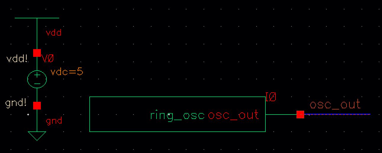
Here is the schematic I used for the simulation above. This schematic uses the symbol from the ring_osc cellview and I added a 5V vdc so the Stimuli was not necessary. I also added an initial condition to the output "osc_out" at 0V using Simulation->Convergence Aids->Initial Condition..

http://cmosedu.com/jbaker/courses/ee421L/f18/students/kiaer/lab7/snip6.JPG

Here is to verify that the extracted view is working the way it is supposed to.

http://cmosedu.com/jbaker/courses/ee421L/f18/students/kiaer/lab7/snip7.JPG

LAB WORK: 

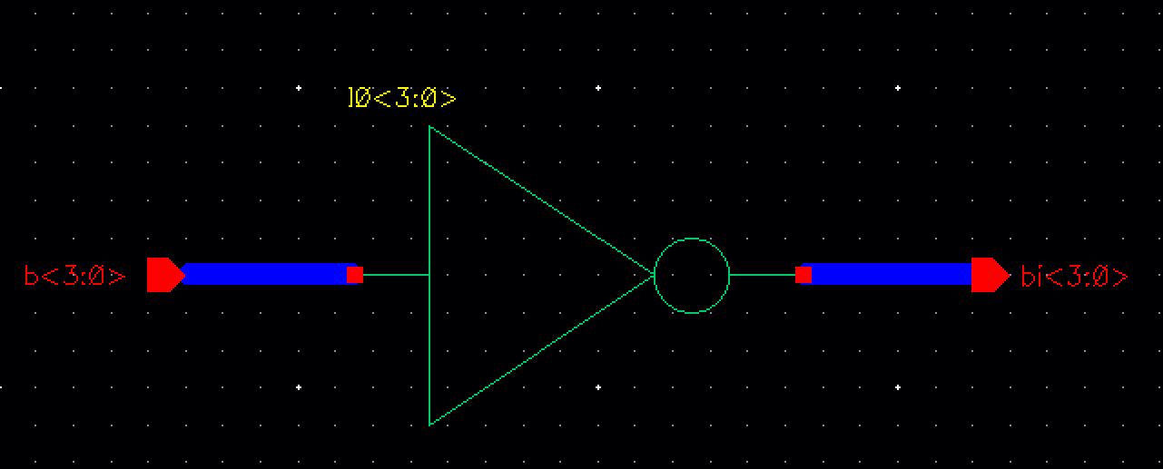
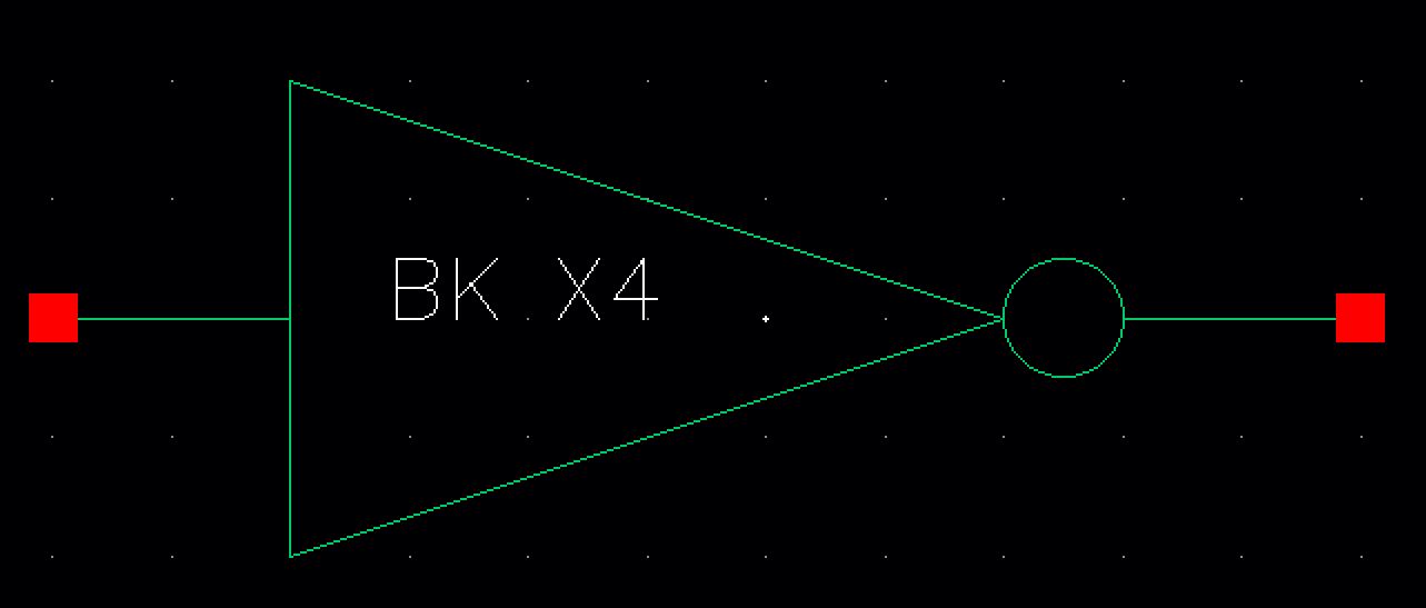
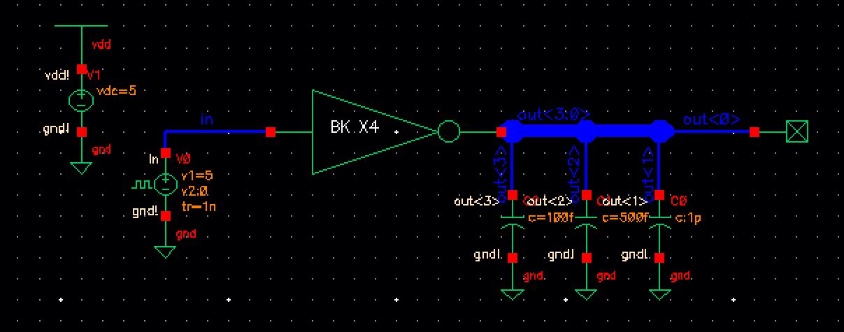
1) Create a 4-bit Inverter 


Here we have the  schematic view of a 4-bit Inverter (left) and the symbol with my initials (right).

http://cmosedu.com/jbaker/courses/ee421L/f18/students/kiaer/lab7/snip8.JPG     http://cmosedu.com/jbaker/courses/ee421L/f18/students/kiaer/lab7/snip9.JPG


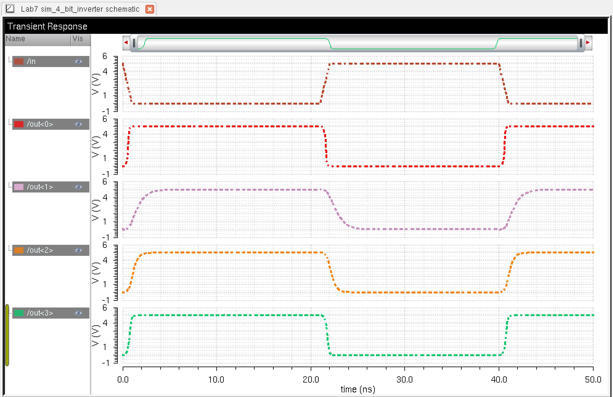
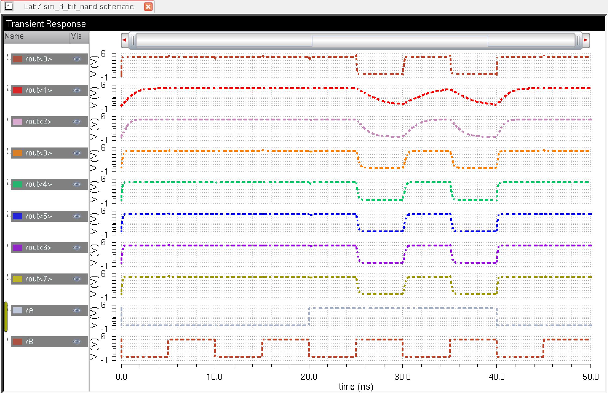
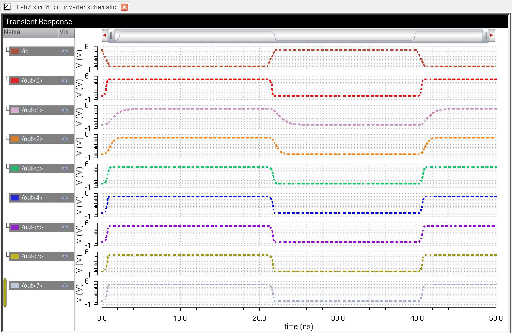
I simulated the results with the capacitive loads indicated in Lab 7. My obervation of the waveforms below show that when a larger load capacitance is added the longer the delay will be. For example, we can see that the output waveform out<1> has the largest capacitor at 1pF and also has the longest delay as well.

http://cmosedu.com/jbaker/courses/ee421L/f18/students/kiaer/lab7/snip10.JPG  http://cmosedu.com/jbaker/courses/ee421L/f18/students/kiaer/lab7/snip11.JPG

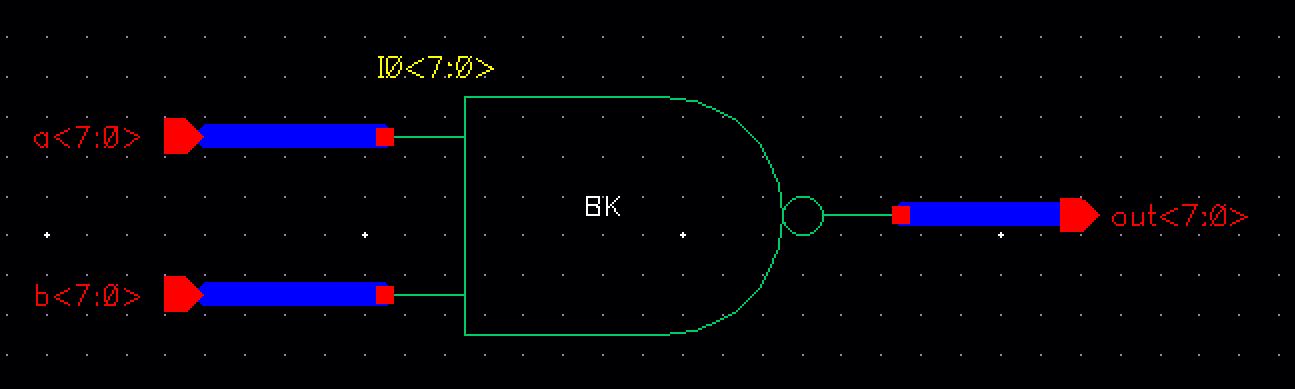
2.) Create schematics and symbols for an 8-bit input/output array of: NAND, NOR, AND, inverter, and OR gates.
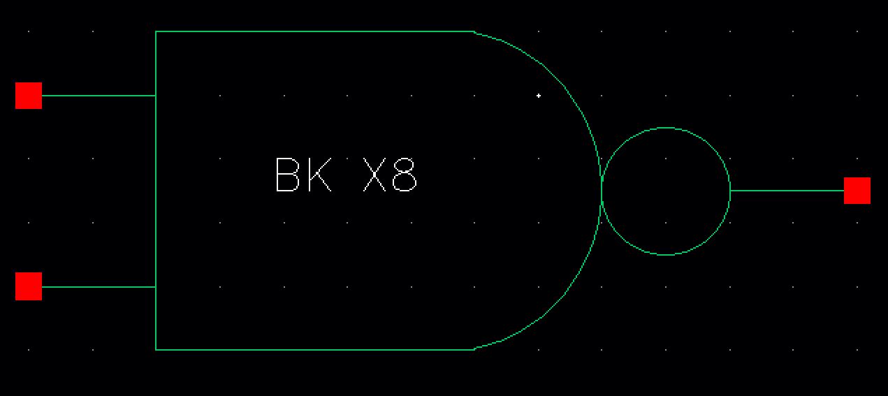
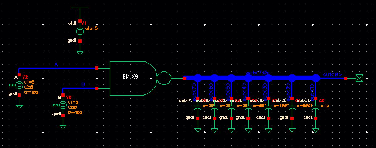
8-bit NAND GATE: 

8-bit NAND Gate schematic and symbol:

http://cmosedu.com/jbaker/courses/ee421L/f18/students/kiaer/lab7/snip12.JPG   http://cmosedu.com/jbaker/courses/ee421L/f18/students/kiaer/lab7/snip13.JPG

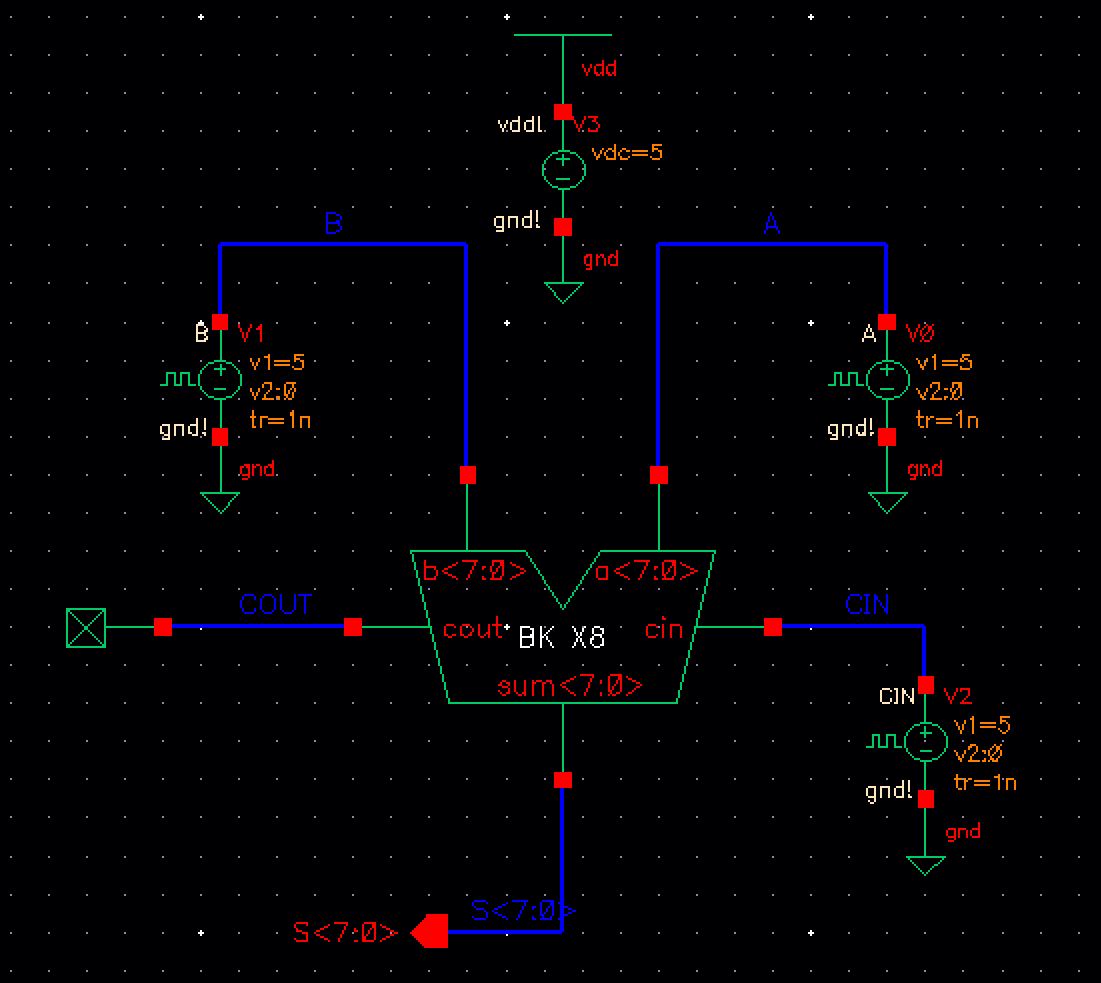
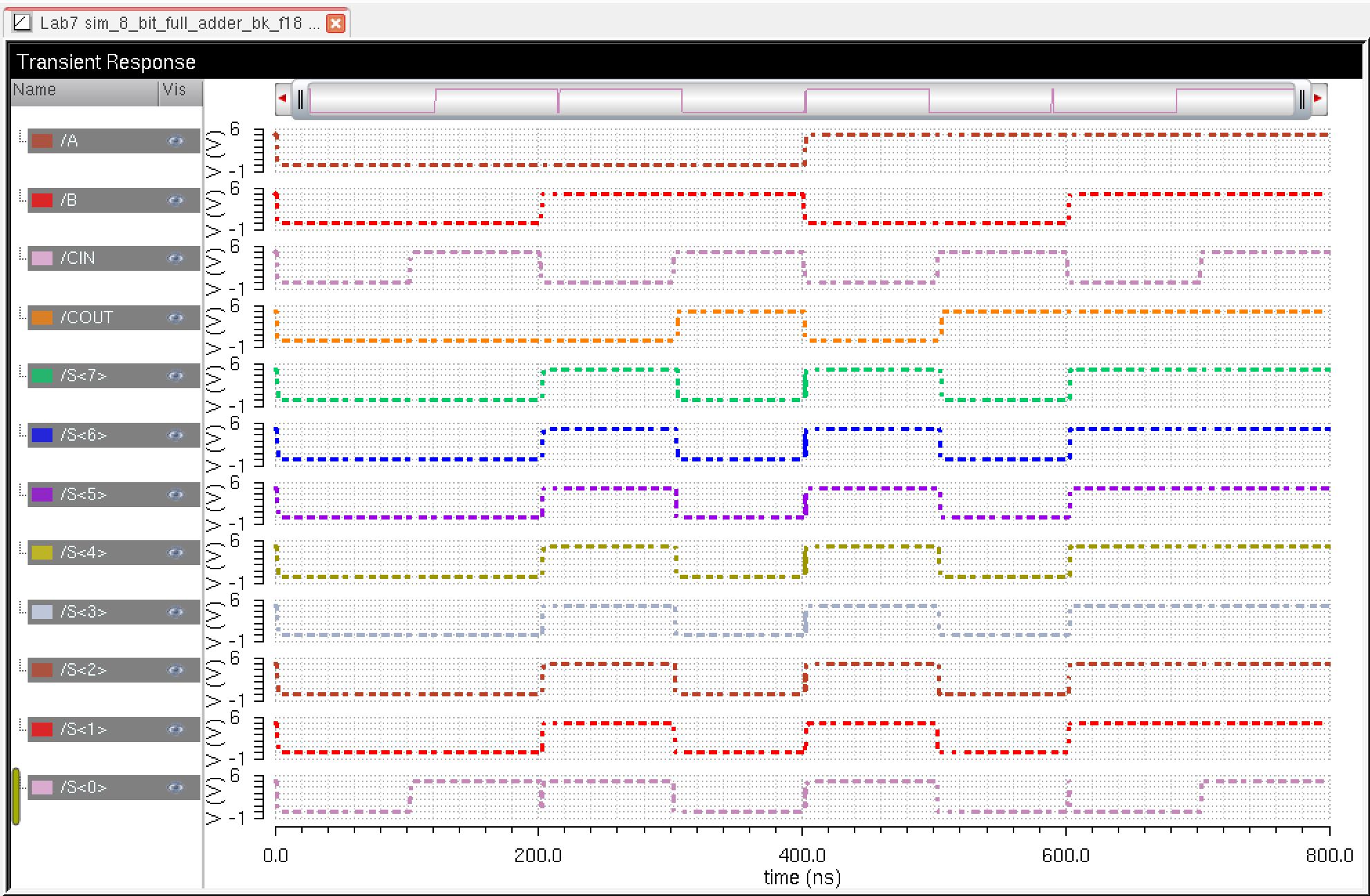
Simulation schematic and respective waveforms: 
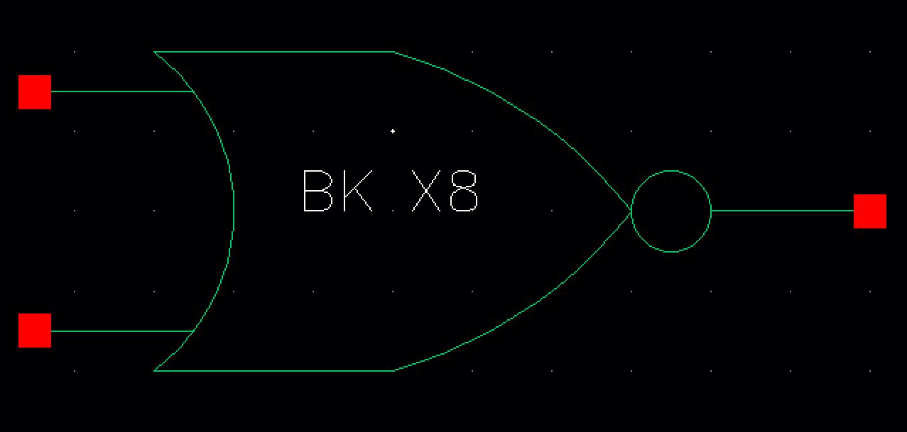
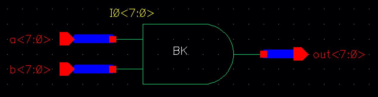
http://cmosedu.com/jbaker/courses/ee421L/f18/students/kiaer/lab7/snip14.JPG http://cmosedu.com/jbaker/courses/ee421L/f18/students/kiaer/lab7/snip15.JPG


8-bit NOR GATE: 

8-bit NOR Gate schematic and symbol

http://cmosedu.com/jbaker/courses/ee421L/f18/students/kiaer/lab7/snip16.JPG  http://cmosedu.com/jbaker/courses/ee421L/f18/students/kiaer/lab7/snip17.JPG

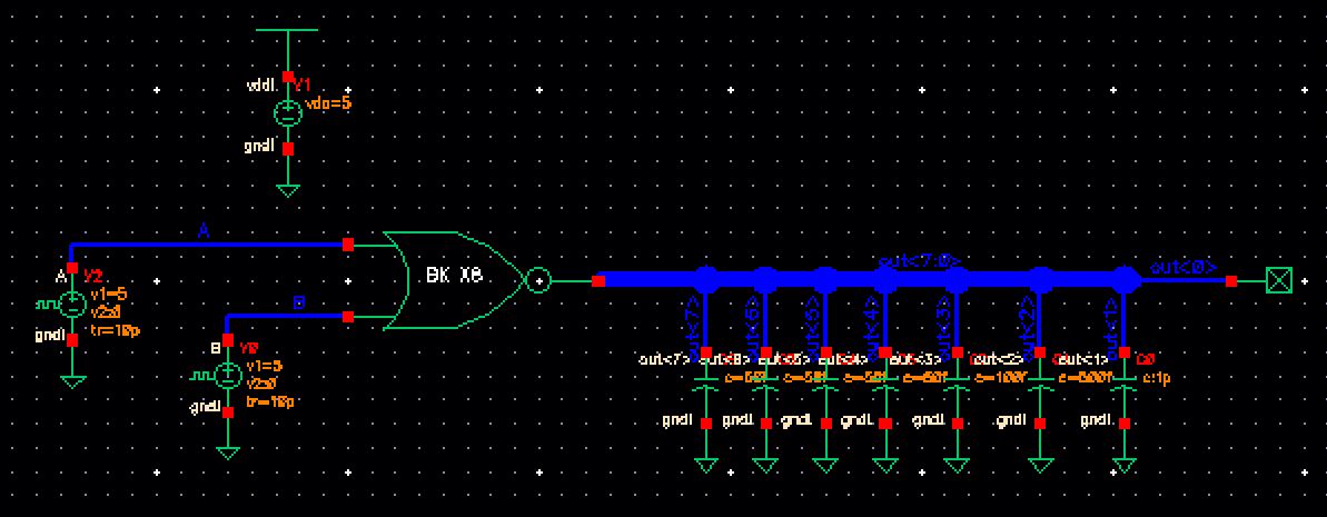
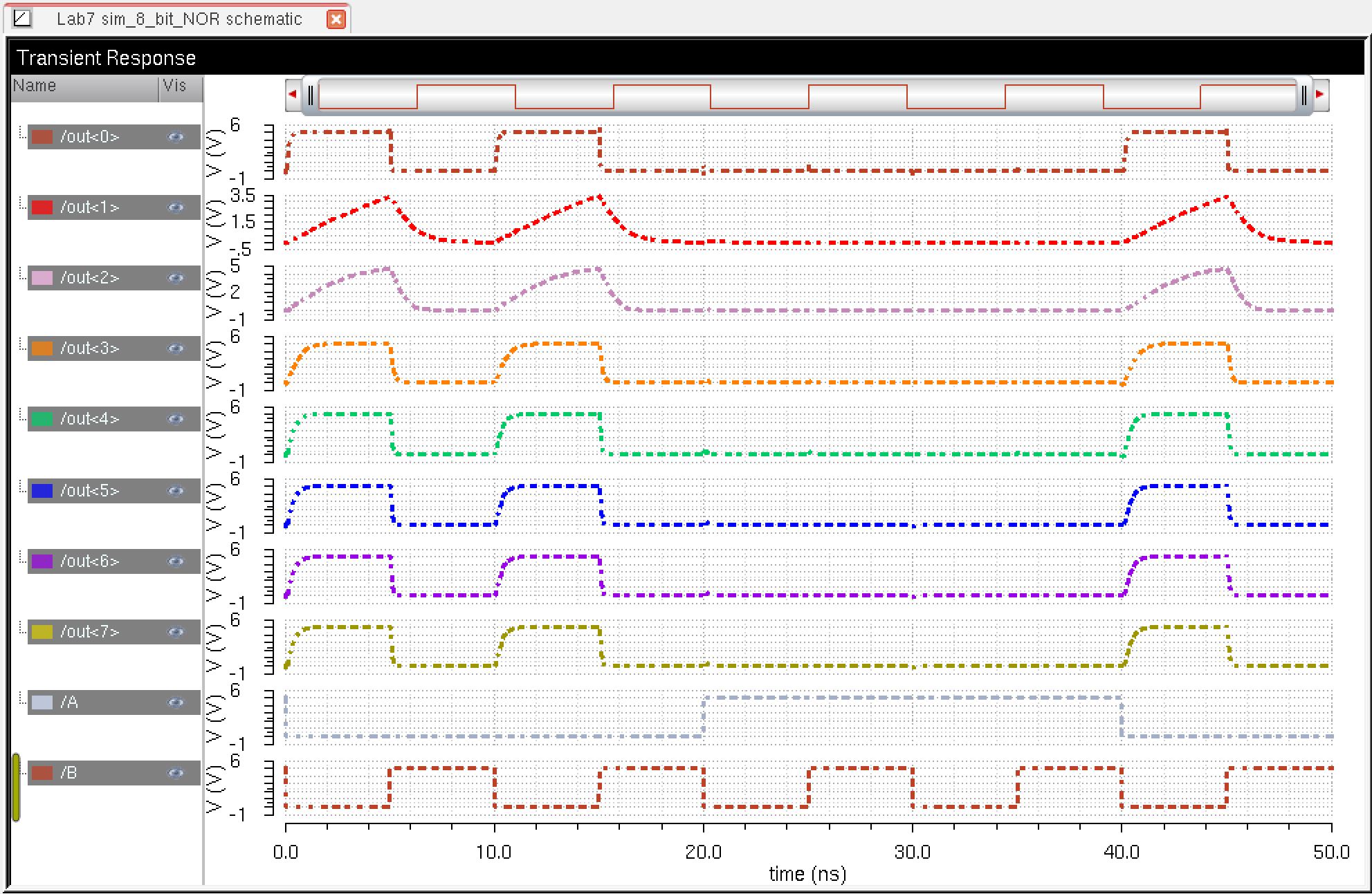
Simulation schematic for 8-bit NOR gate and respective waveforms
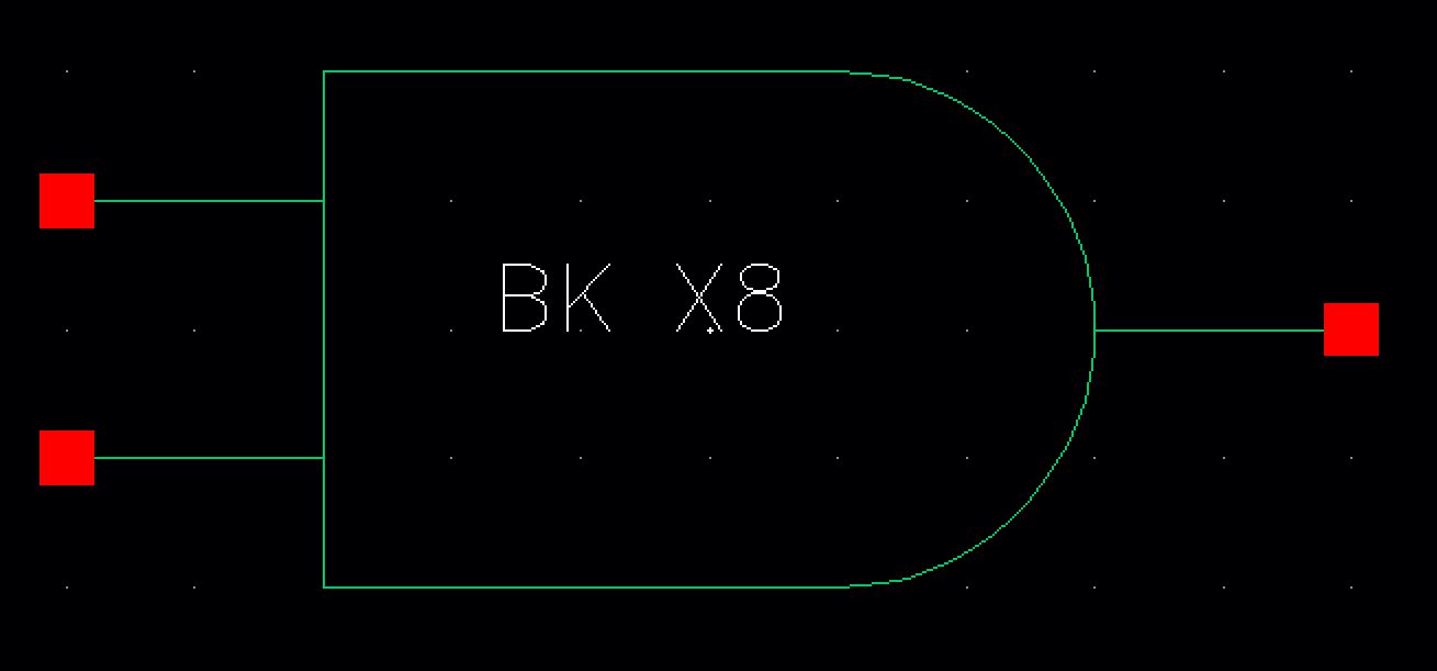
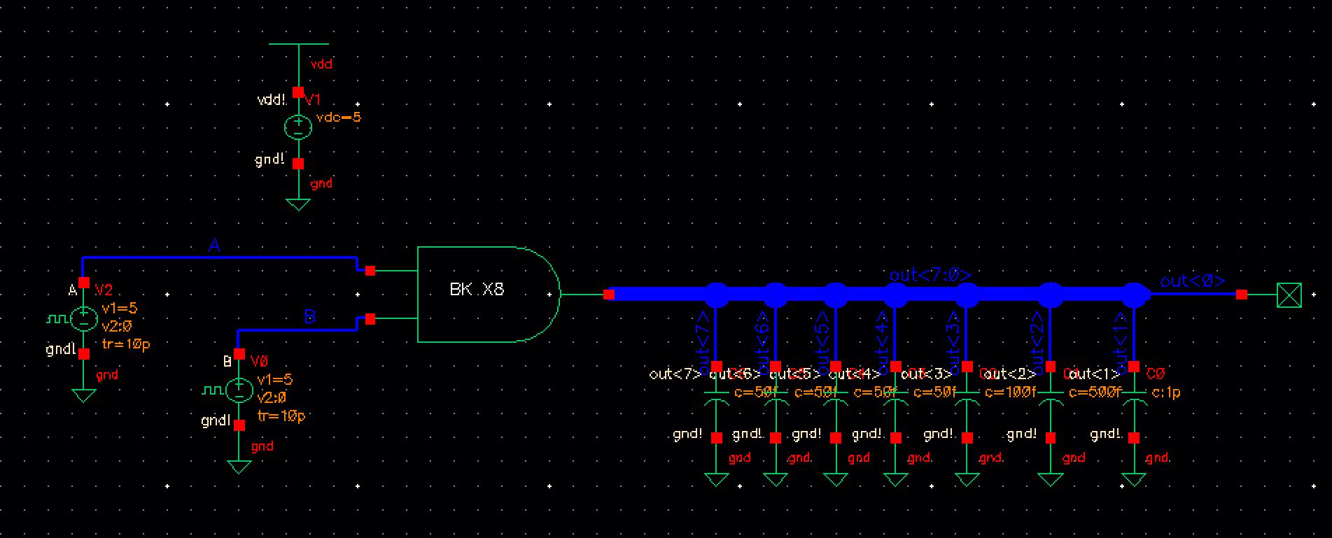
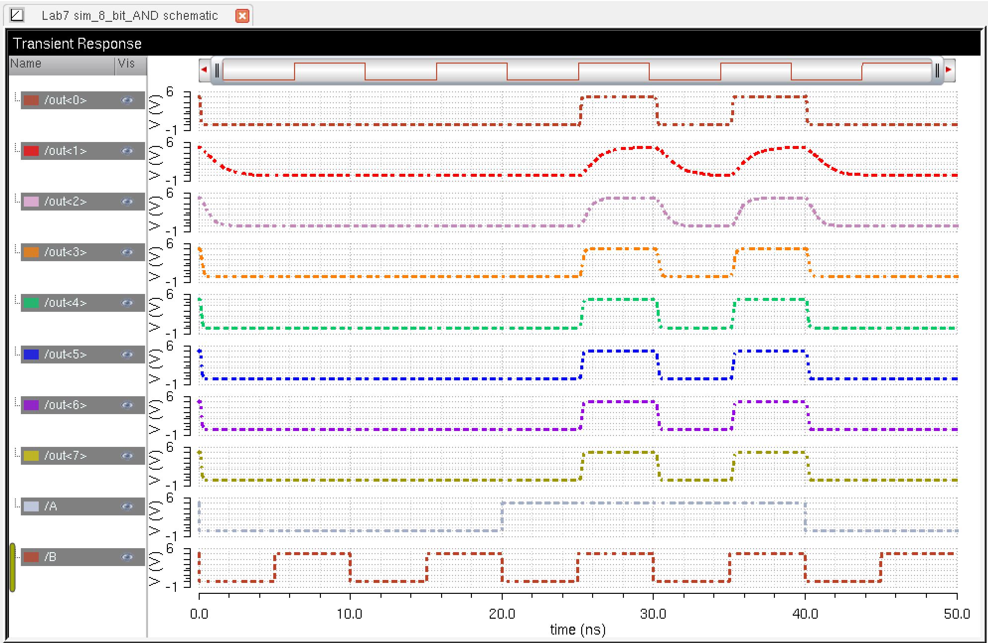
http://cmosedu.com/jbaker/courses/ee421L/f18/students/kiaer/lab7/snip18.JPG  http://cmosedu.com/jbaker/courses/ee421L/f18/students/kiaer/lab7/snip19.JPG

8-bit AND GATE:

8-bit AND gate and symbol
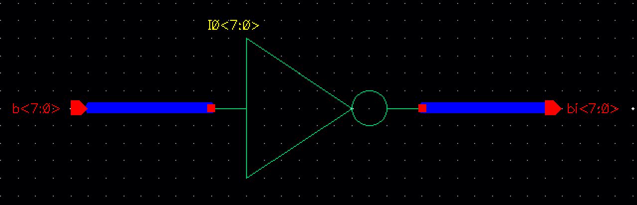
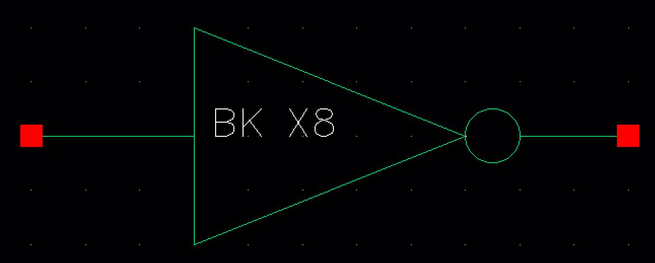
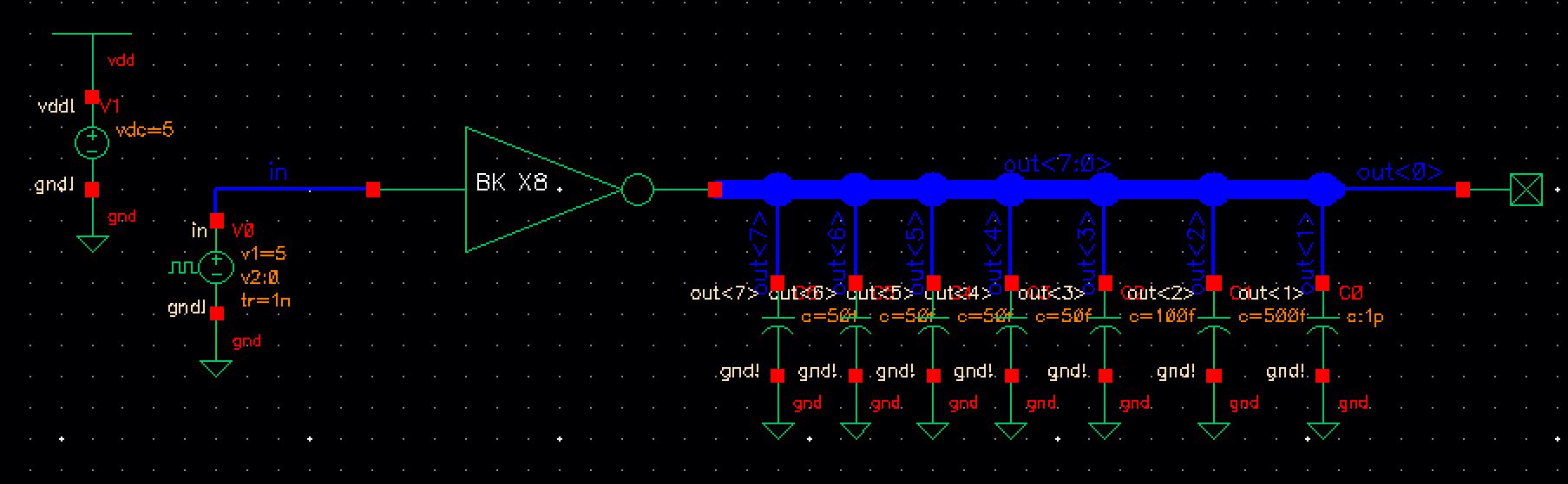
http://cmosedu.com/jbaker/courses/ee421L/f18/students/kiaer/lab7/snip20.JPG  http://cmosedu.com/jbaker/courses/ee421L/f18/students/kiaer/lab7/snip21.JPG


Simulation schematic for 8-bit AND gate and respective waveforms

http://cmosedu.com/jbaker/courses/ee421L/f18/students/kiaer/lab7/snip22.JPG http://cmosedu.com/jbaker/courses/ee421L/f18/students/kiaer/lab7/snip23.JPG

8-bit INVERTER:

8-bit Inverter schematic and symbol
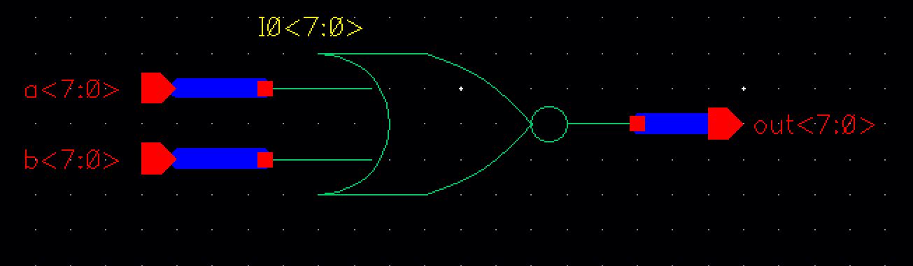
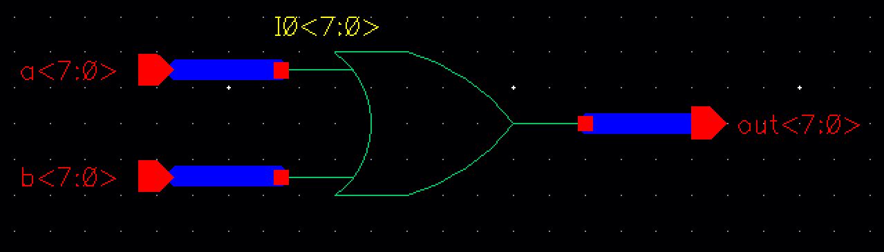
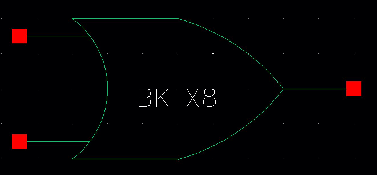
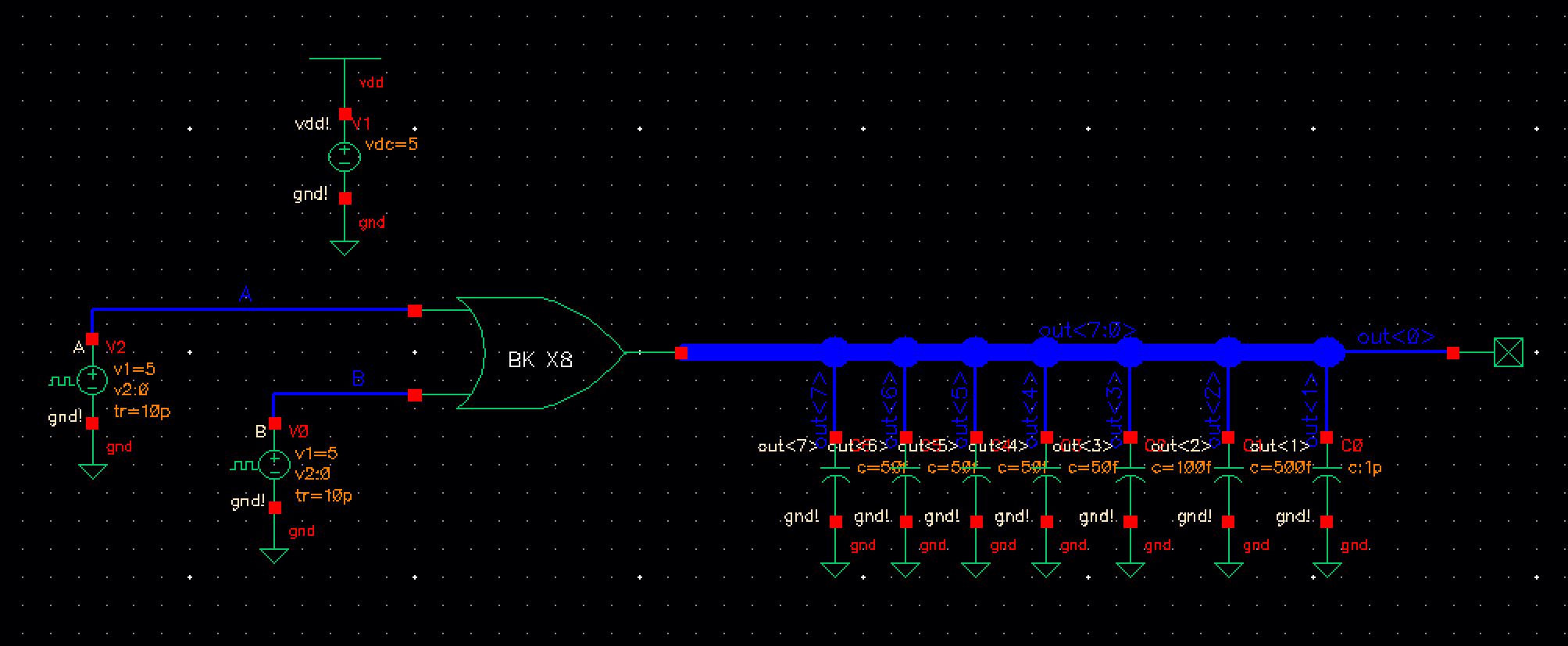
http://cmosedu.com/jbaker/courses/ee421L/f18/students/kiaer/lab7/snip24.JPG  http://cmosedu.com/jbaker/courses/ee421L/f18/students/kiaer/lab7/snip25.JPG

Simulation schematic for 8-bit Inverter and respective waveforms

http://cmosedu.com/jbaker/courses/ee421L/f18/students/kiaer/lab7/snip26.JPG  http://cmosedu.com/jbaker/courses/ee421L/f18/students/kiaer/lab7/snip27.JPG

8-bit OR GATE:

8-bit OR Gate schematic and symbol

http://cmosedu.com/jbaker/courses/ee421L/f18/students/kiaer/lab7/snip28.JPG http://cmosedu.com/jbaker/courses/ee421L/f18/students/kiaer/lab7/snip29.JPG

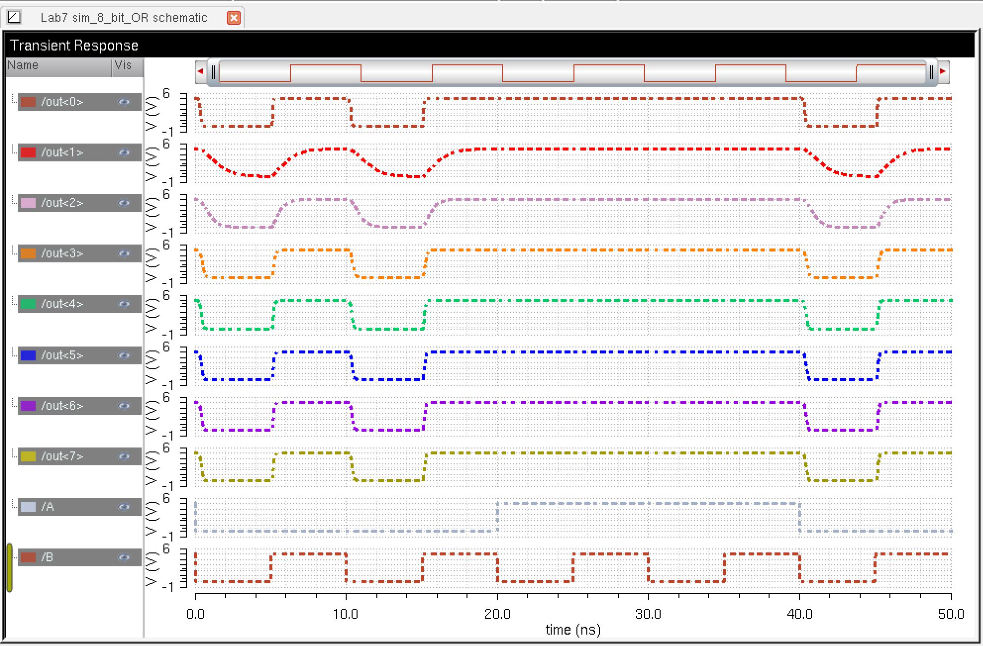
Simulation schematic for 8-bit OR Gate and respective waveforms

http://cmosedu.com/jbaker/courses/ee421L/f18/students/kiaer/lab7/snip30.JPG http://cmosedu.com/jbaker/courses/ee421L/f18/students/kiaer/lab7/snip31.JPG

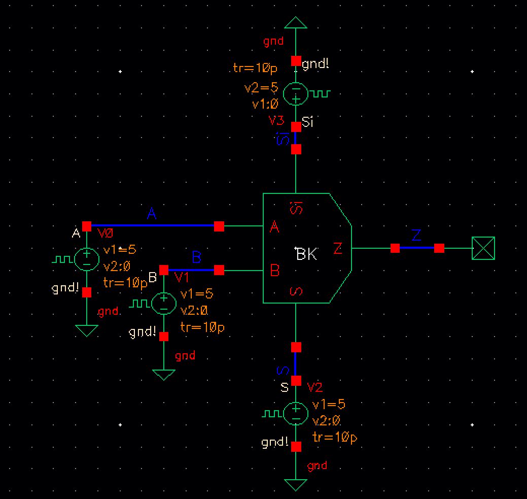
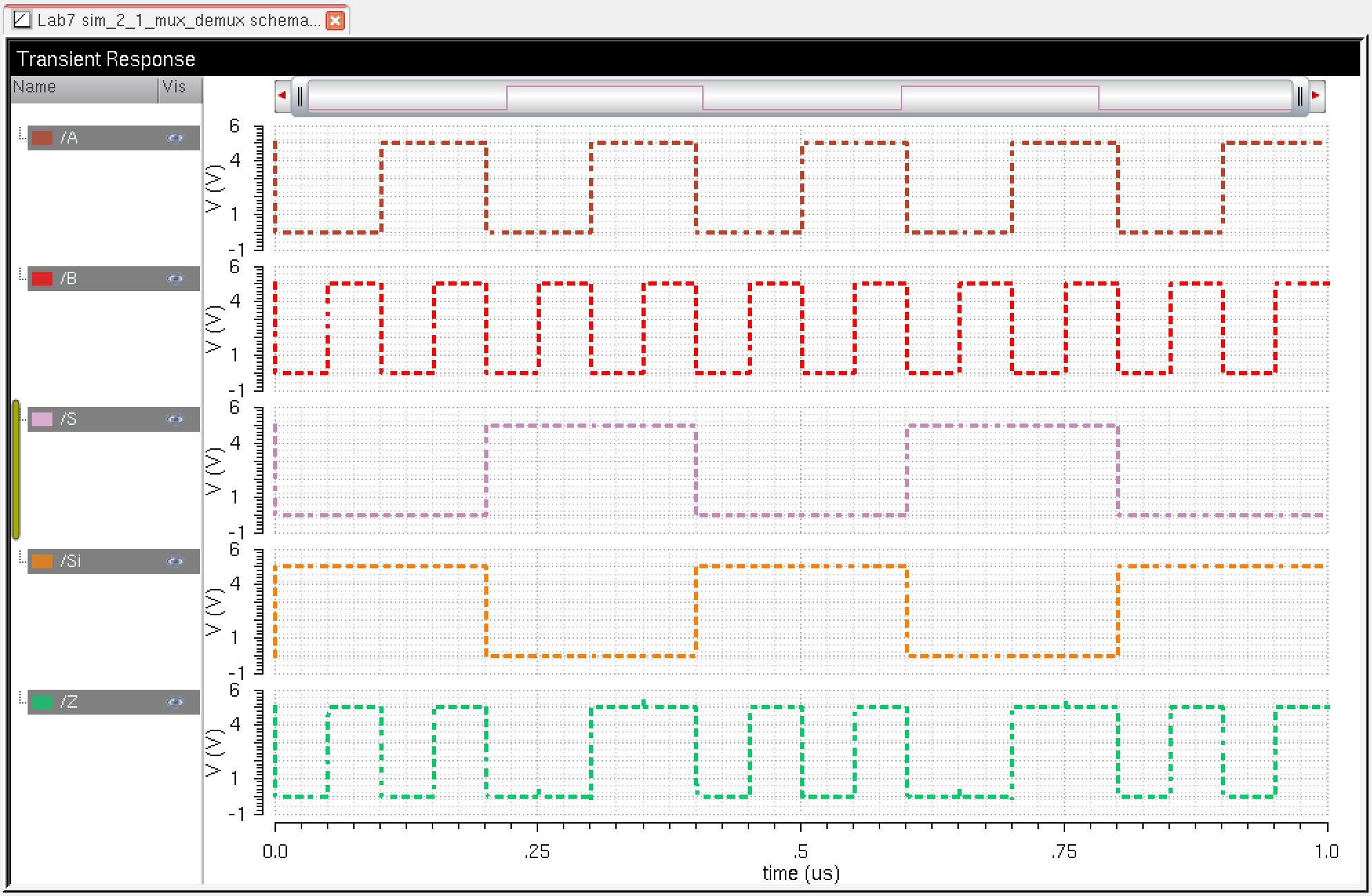
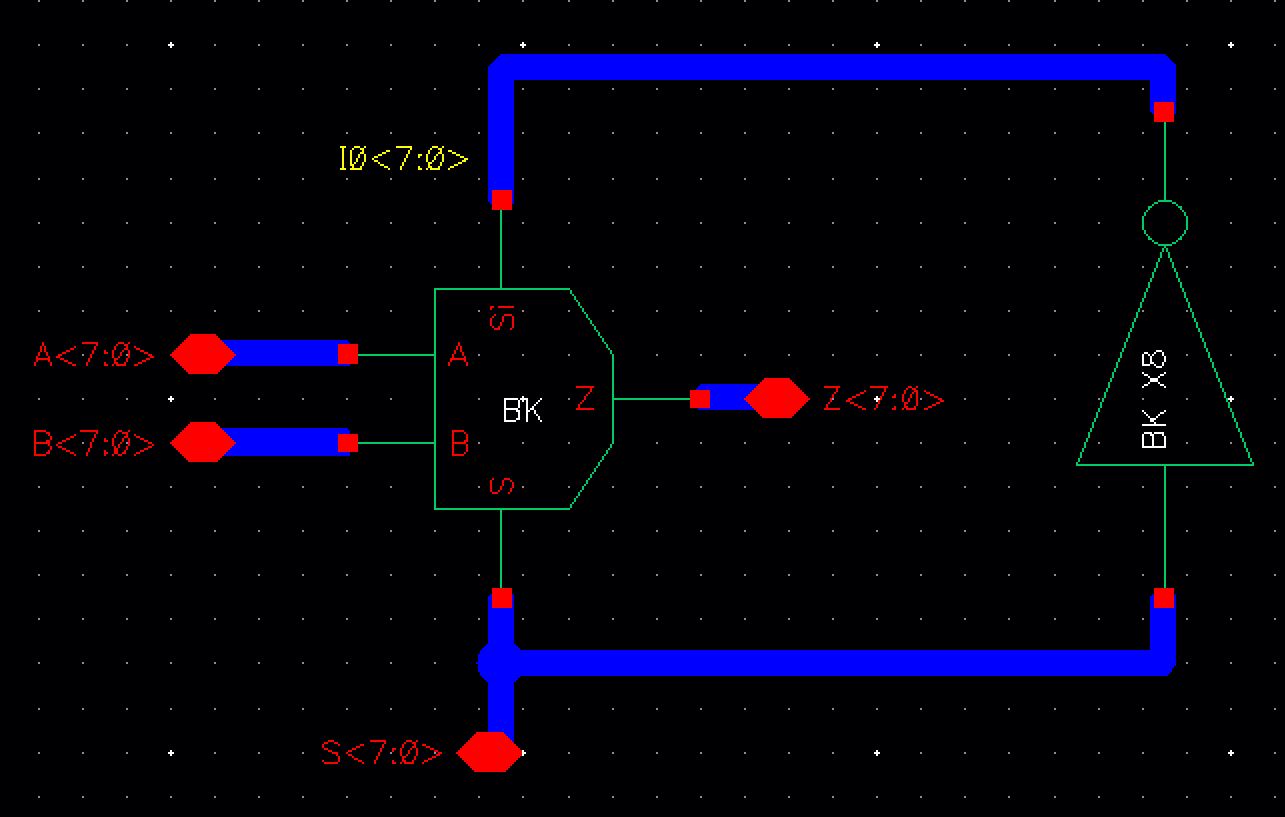
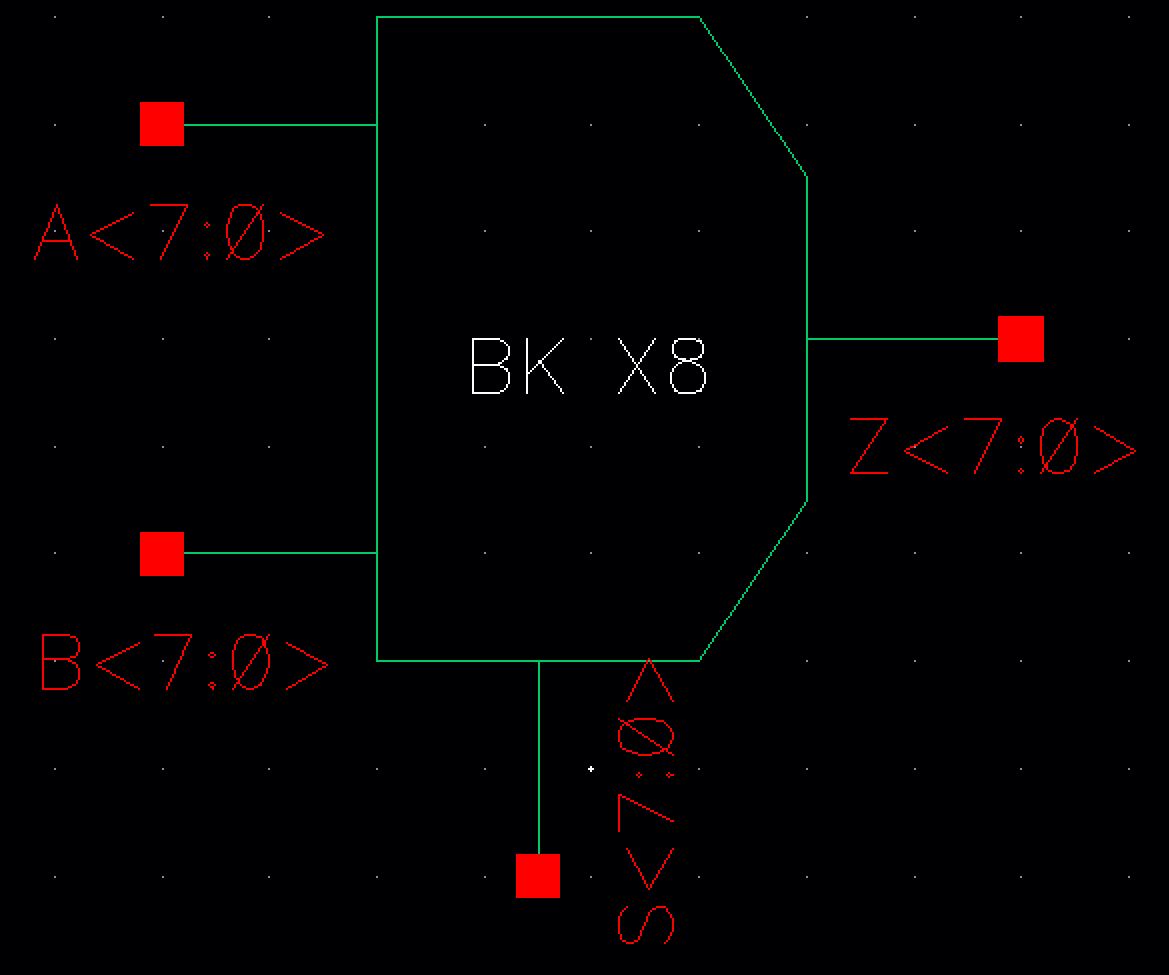
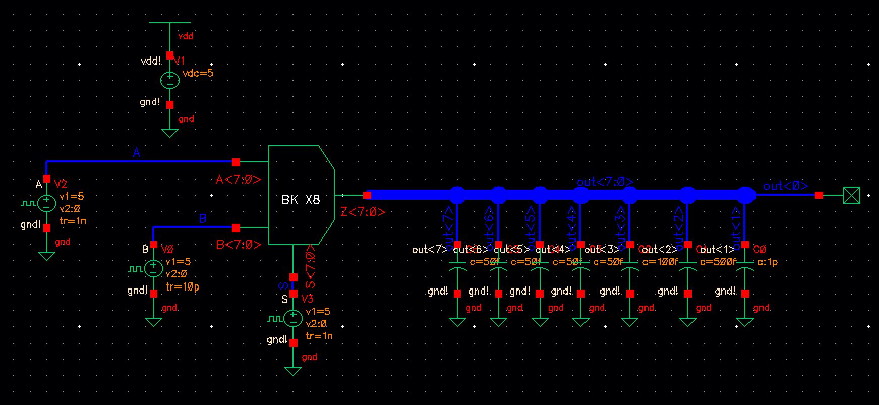
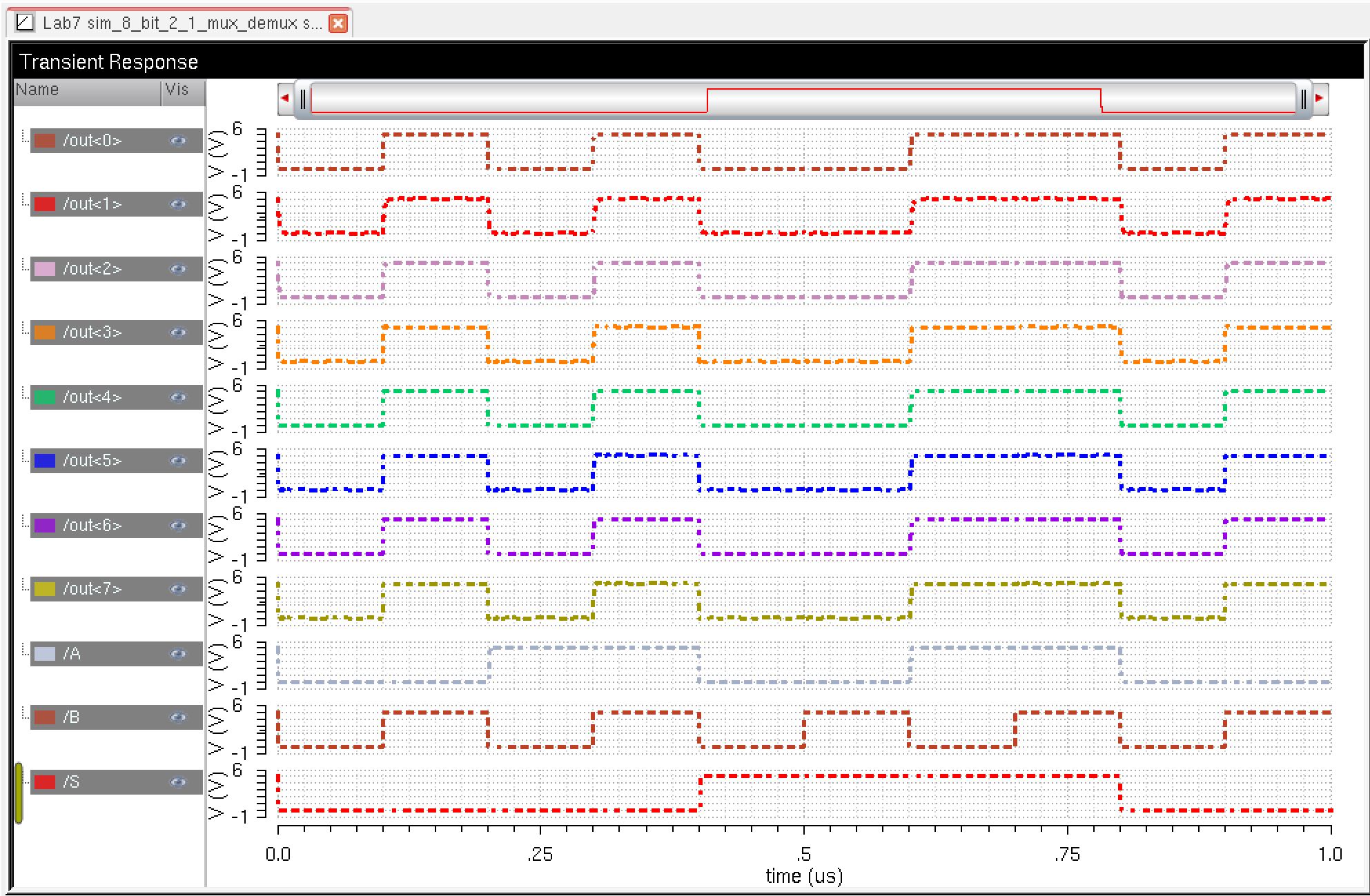
3) Create a 2-to-1 MUX/DEMUX 

2-to-1 MUX/DEMUX Schematic and Symbol


http://cmosedu.com/jbaker/courses/ee421L/f18/students/kiaer/lab7/snip32.JPG  http://cmosedu.com/jbaker/courses/ee421L/f18/students/kiaer/lab7/snip33.JPG

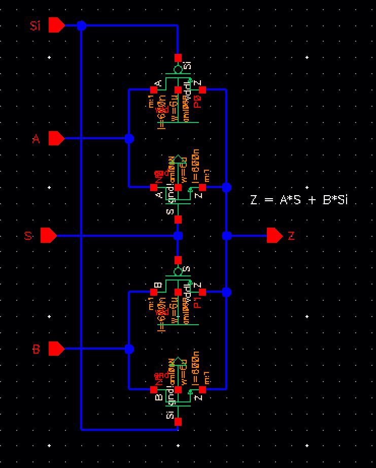
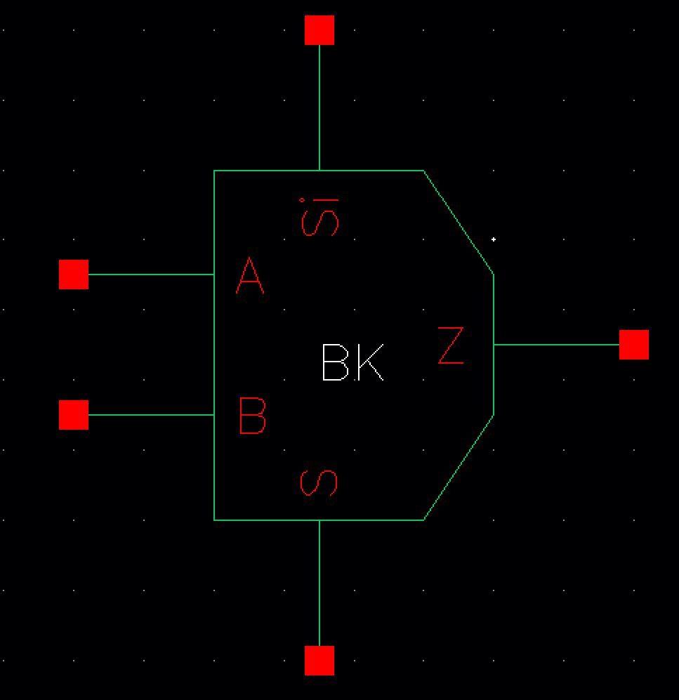
The multiplexer/demux works by turning on a specific TG at a time. For example below, when S is high the output Z is B and when Si is high (S is low) the output Z is equal to A.


http://cmosedu.com/jbaker/courses/ee421L/f18/students/kiaer/lab7/snip34.JPG   http://cmosedu.com/jbaker/courses/ee421L/f18/students/kiaer/lab7/snip35.JPG


4) Create an 8-bit wide word 2-to-1 MUX/DEMUX schematic and symbol: 

8-bit 2-to-1 MUX/DEMUX schematic and symbol


  http://cmosedu.com/jbaker/courses/ee421L/f18/students/kiaer/lab7/snip36.JPG http://cmosedu.com/jbaker/courses/ee421L/f18/students/kiaer/lab7/snip37.JPG

Simulation schematic of 8-bit 2-to-1 MUX/DEMUX and Waveform

http://cmosedu.com/jbaker/courses/ee421L/f18/students/kiaer/lab7/snip38.JPG


http://cmosedu.com/jbaker/courses/ee421L/f18/students/kiaer/lab7/snip39.JPG


5.) Create an 8-bit Full Adder

Schematic using the Full Adder symbol from Lab 6 to create the schematic for an 8-bit Full Adder.

http://cmosedu.com/jbaker/courses/ee421L/f18/students/kiaer/lab7/snip40.JPG  http://cmosedu.com/jbaker/courses/ee421L/f18/students/kiaer/lab7/snip41.JPG

http://cmosedu.com/jbaker/courses/ee421L/f18/students/kiaer/lab7/snip42.JPG  http://cmosedu.com/jbaker/courses/ee421L/f18/students/kiaer/lab7/snip43.JPG

6) Layout the Full Adder with DRC and LVS.


Full Layout:
http://cmosedu.com/jbaker/courses/ee421L/f18/students/kiaer/lab7/snip44.JPG

Left Side (bit 0)  - Also using metal3 connections, cout of the first FA is connected to the second FA's cin.

http://cmosedu.com/jbaker/courses/ee421L/f18/students/kiaer/lab7/snip45.JPG


Right Side (bit 7)
http://cmosedu.com/jbaker/courses/ee421L/f18/students/kiaer/lab7/snip46.JPG

Extracted View (Full)

 http://cmosedu.com/jbaker/courses/ee421L/f18/students/kiaer/lab7/snip47.JPG

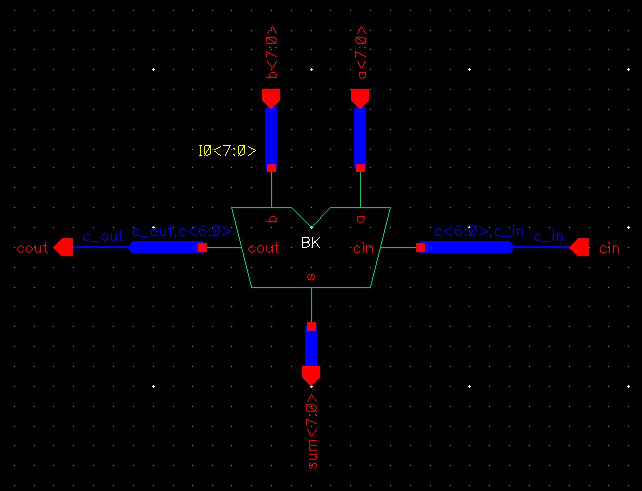
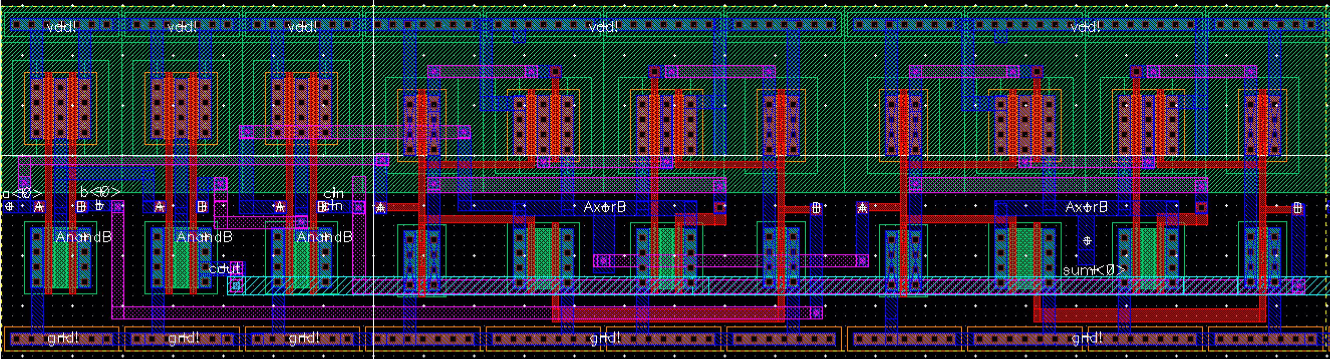
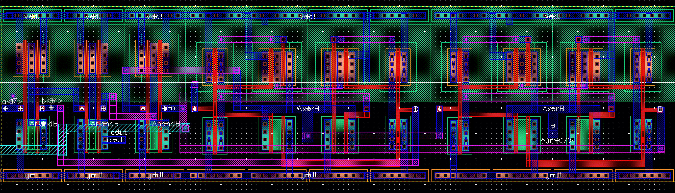
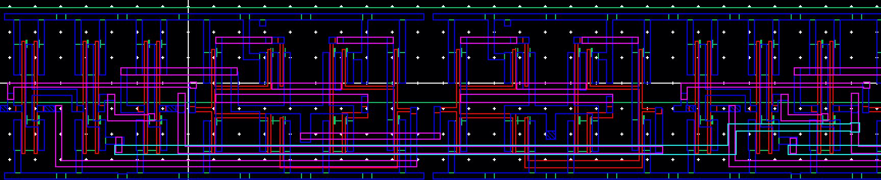
One FA showing metal3 connection to second FA

http://cmosedu.com/jbaker/courses/ee421L/f18/students/kiaer/lab7/snip48.JPG

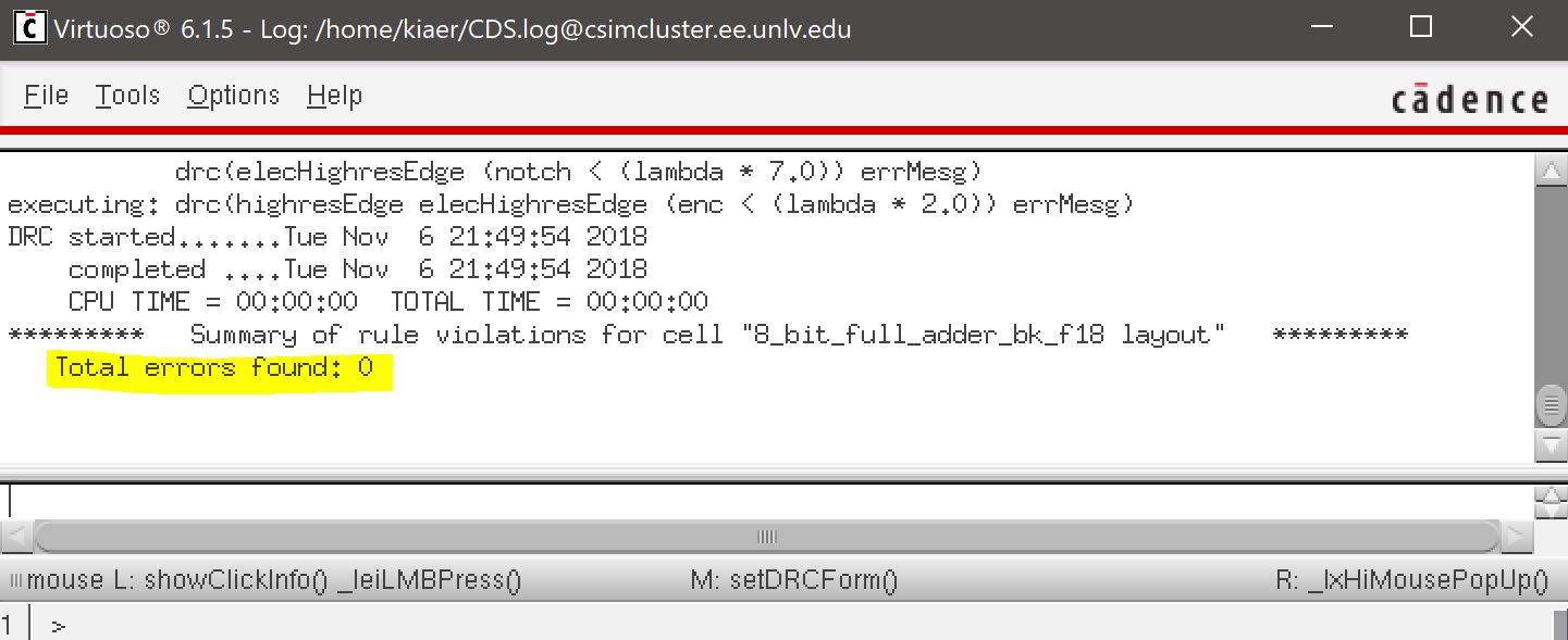
DRC Verification for 8-bit Full Adder.

http://cmosedu.com/jbaker/courses/ee421L/f18/students/kiaer/lab7/snip49.JPG

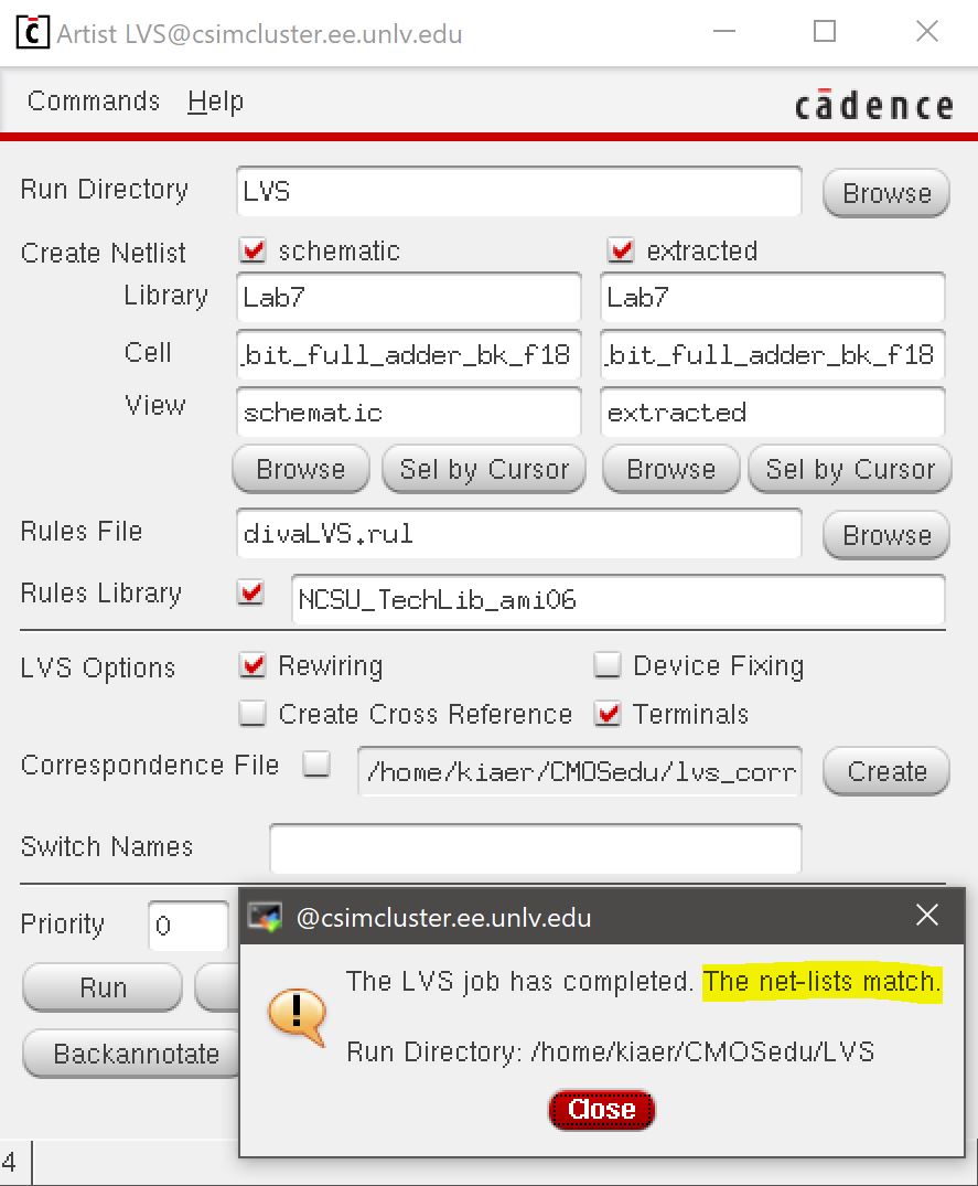
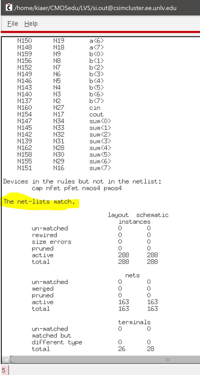
LVS verification of 8-bit Full Adder

http://cmosedu.com/jbaker/courses/ee421L/f18/students/kiaer/lab7/snip50.JPG  http://cmosedu.com/jbaker/courses/ee421L/f18/students/kiaer/lab7/snip51.JPG


My design directory can be found here: Lab7.zip

Return to Brian's Labs