Lab 6 - ECE 421L
Brian Medrano Kiaer
Email: kiaer@unlv.nevada.edu
October 18, 2018
Prelab Work:
The
purpose of the Lab 6 prelab is to learn how to create a NAND Gate in a
schematic and a layout then DRC and LVS those two.
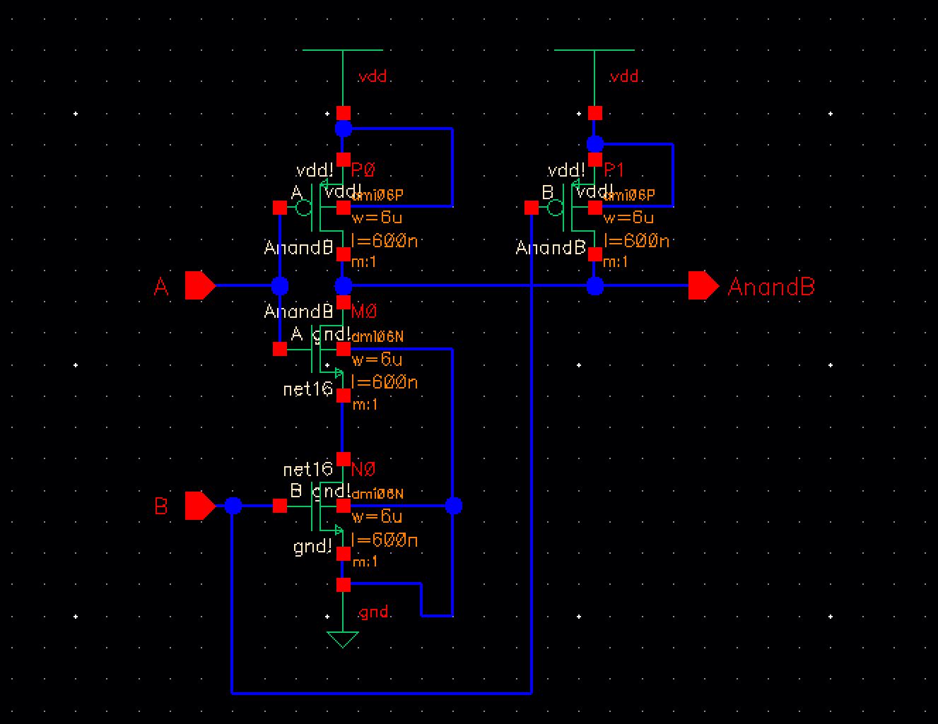
Above is the NAND2 Gate Schematic created from Tutorial_4
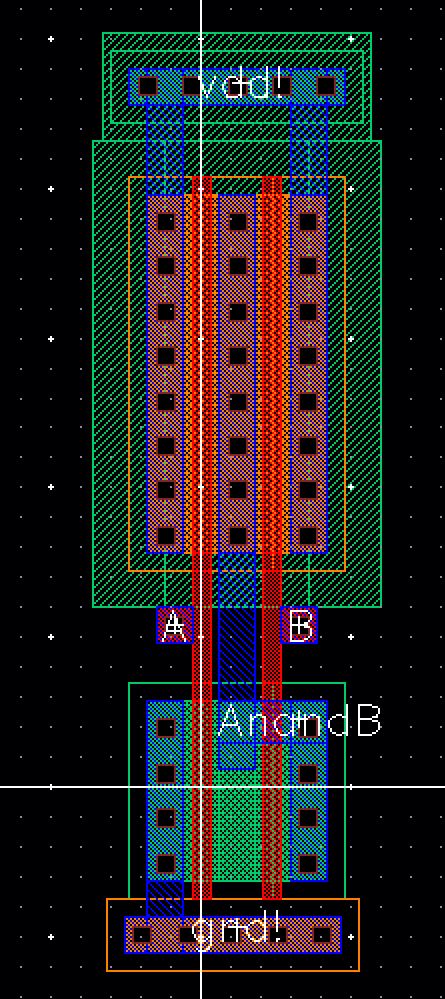
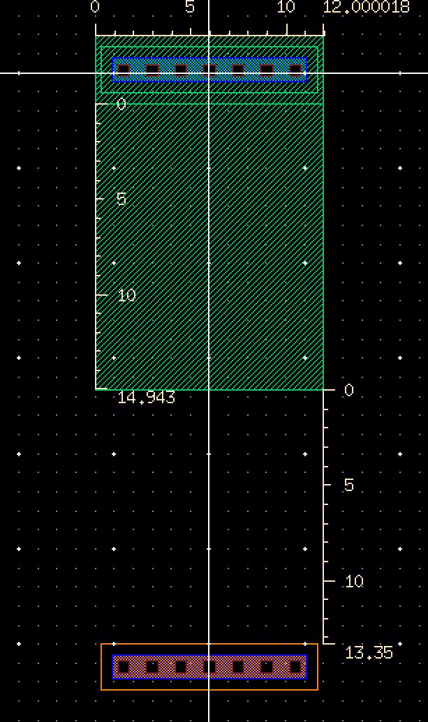
Above is the layout created for the NAND2 Gate created from Tutorial_4
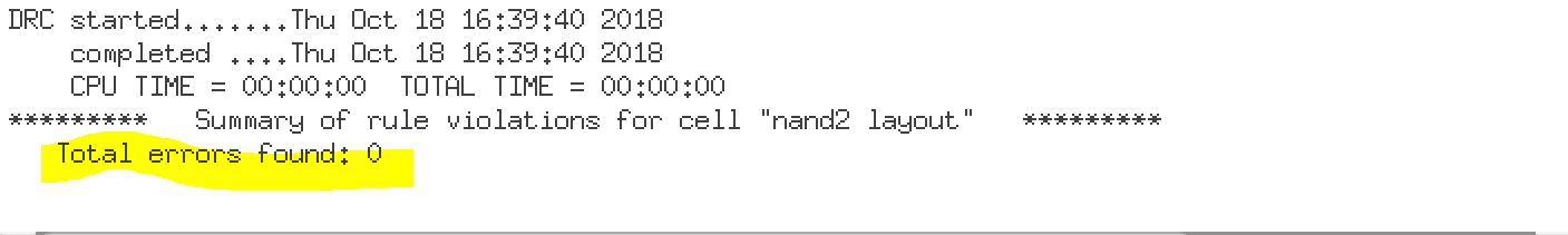
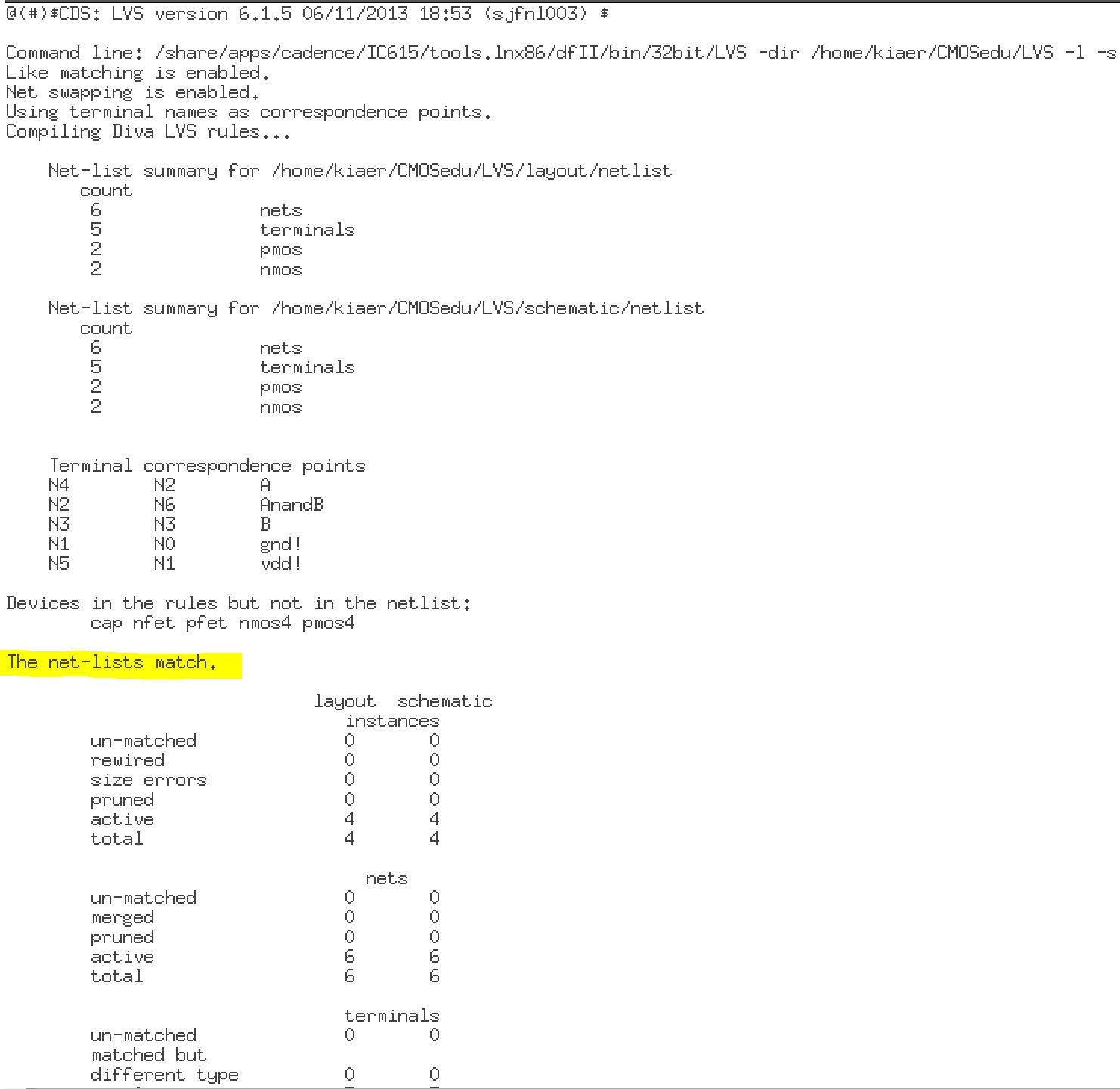
Here
I performed DRC (Verify->DRC) and LVS (Verify->LVS) to ensure
that the schematic and the extracted NAND2 Gates correspond to each
other efficiently.
Lab Work:
Draft the schematics of a 2-input NAND gate and a 2-input XOR gate using 6u/0.6u MOSFETs
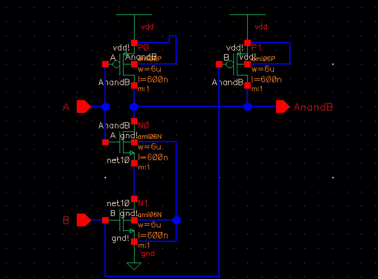
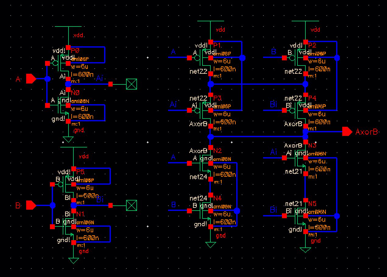
The schematic of a 2-input NAND gate (left) and a 2-input XOR gate (right).
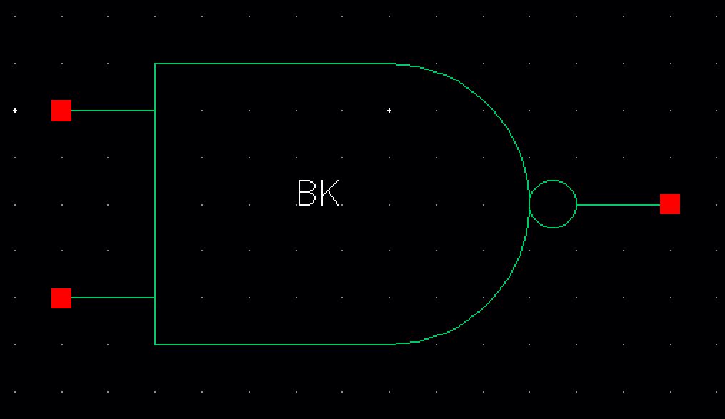
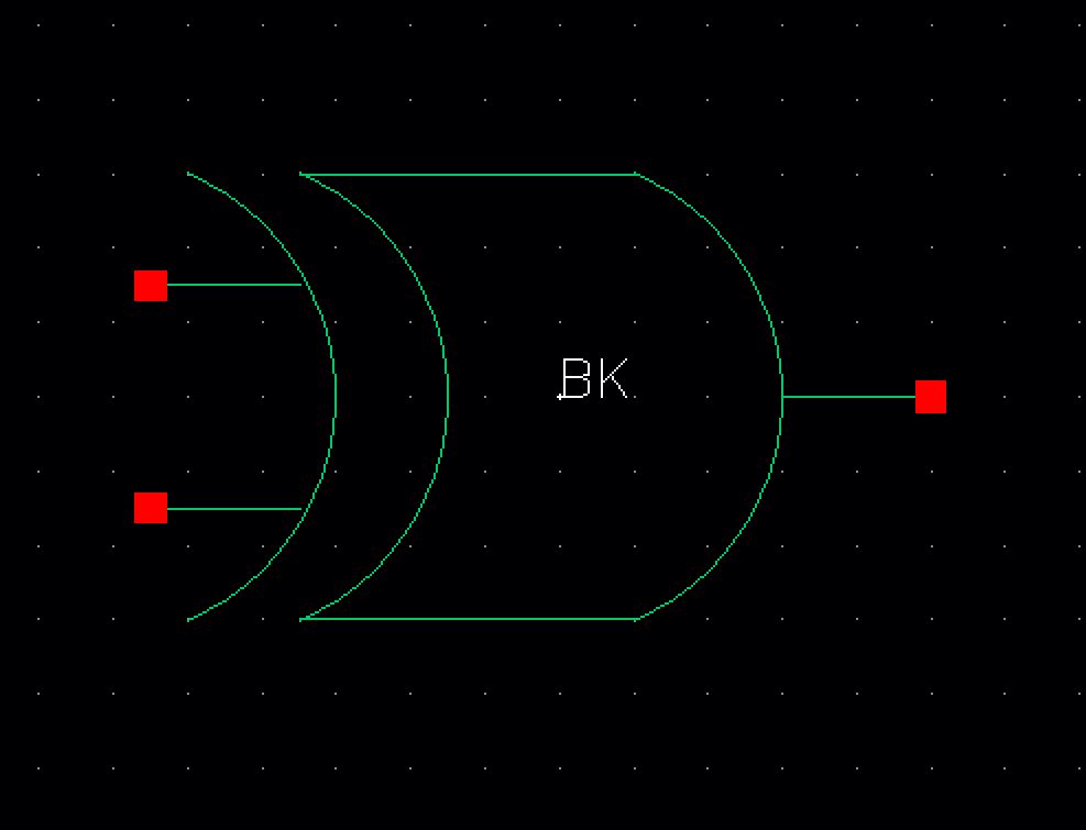
The
symbol cellviews for the 2-input NAND gate (left) and the 2-input XOR
gate (right) with my initials within the symbols using Create ->
Note -> Text.
Before creating the layouts for the NAND gate and the XOR gate. I created a standard cell frame that is taller than previous frames to ensure that I can use it for future assignments and projects.
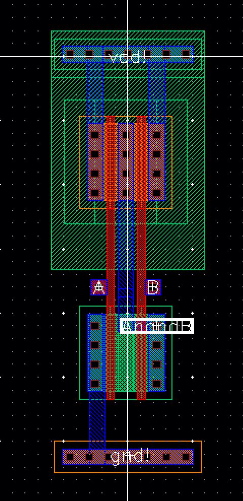
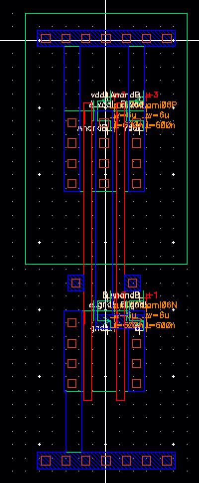
The layout view for the NAND gate (left) and the extracted view of the NAND gate (right)
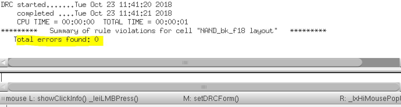
Next I performed a DRC check to ensure that there are no issues with the layout (Verify -> DRC).
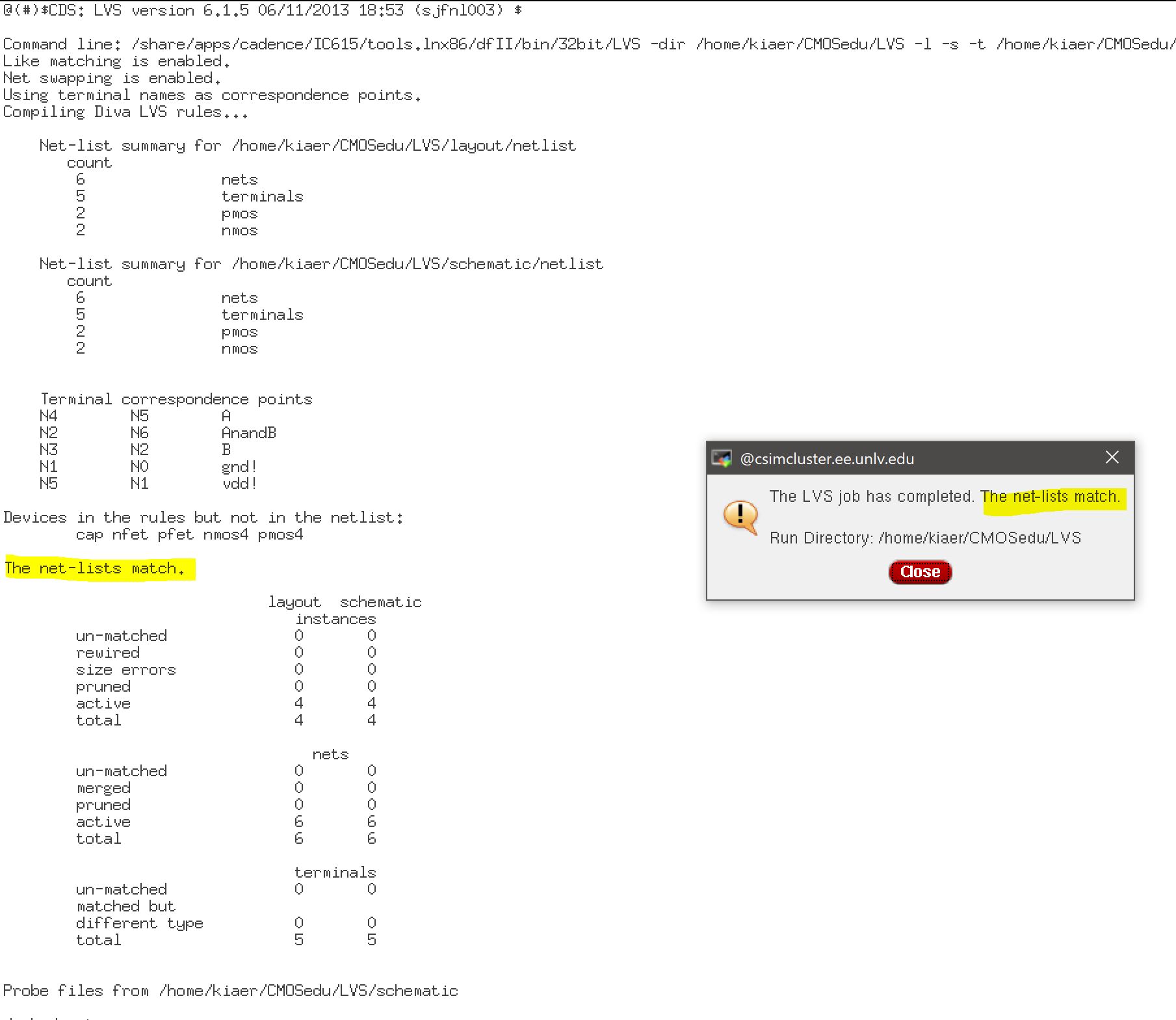
Then I ran LVS (Verify->LVS) to ensure that there are no discrepancies between the schematic and the extracted view of the NAND gate.
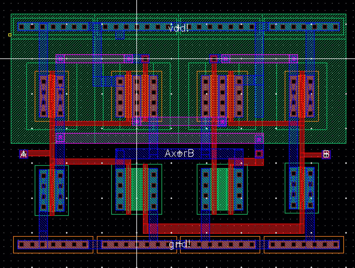
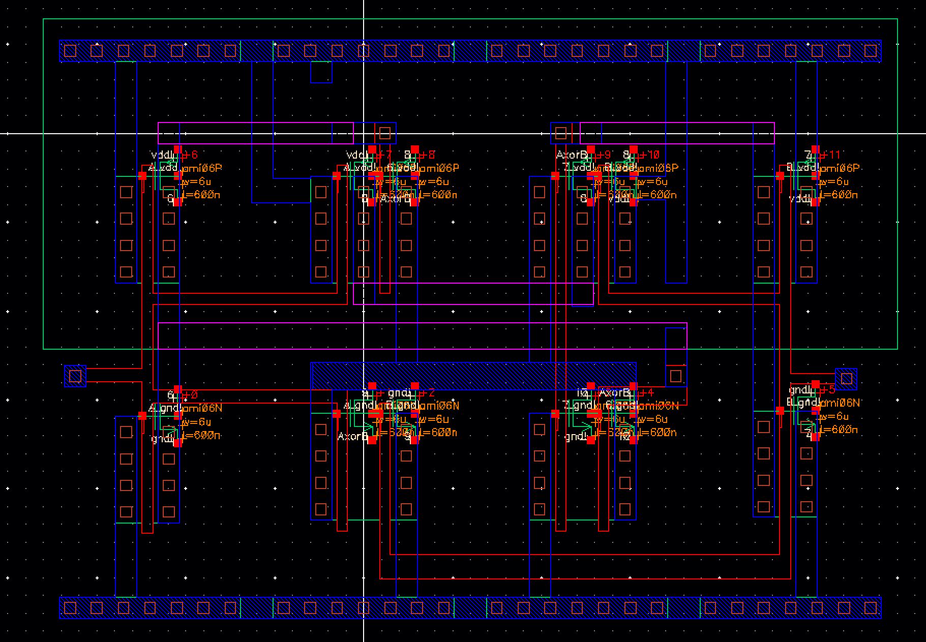
The layout above is for the 2-input XOR gate (left) and the extracted view of the layout for the 2-input XOR gate (right)
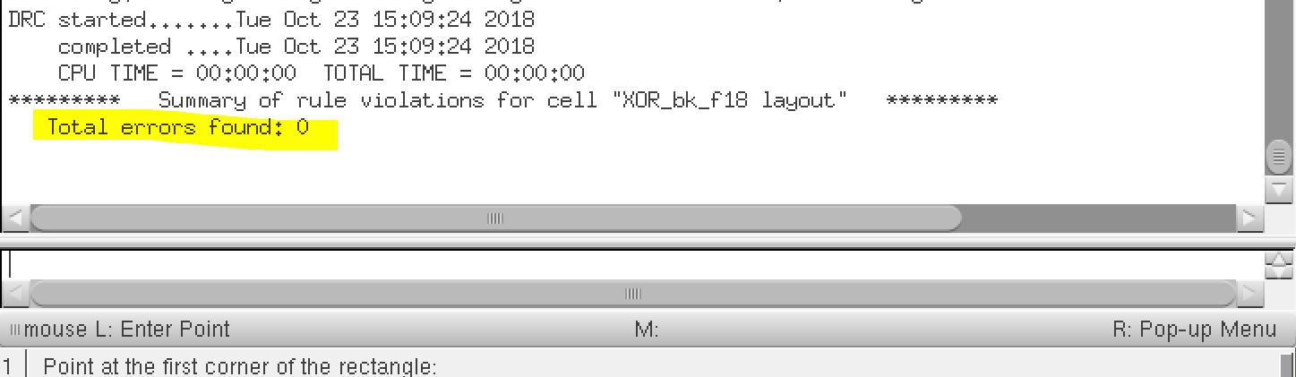
I ran DRC and LVS on the layout to ensure there are no issues with the layout. The net-lists matched.
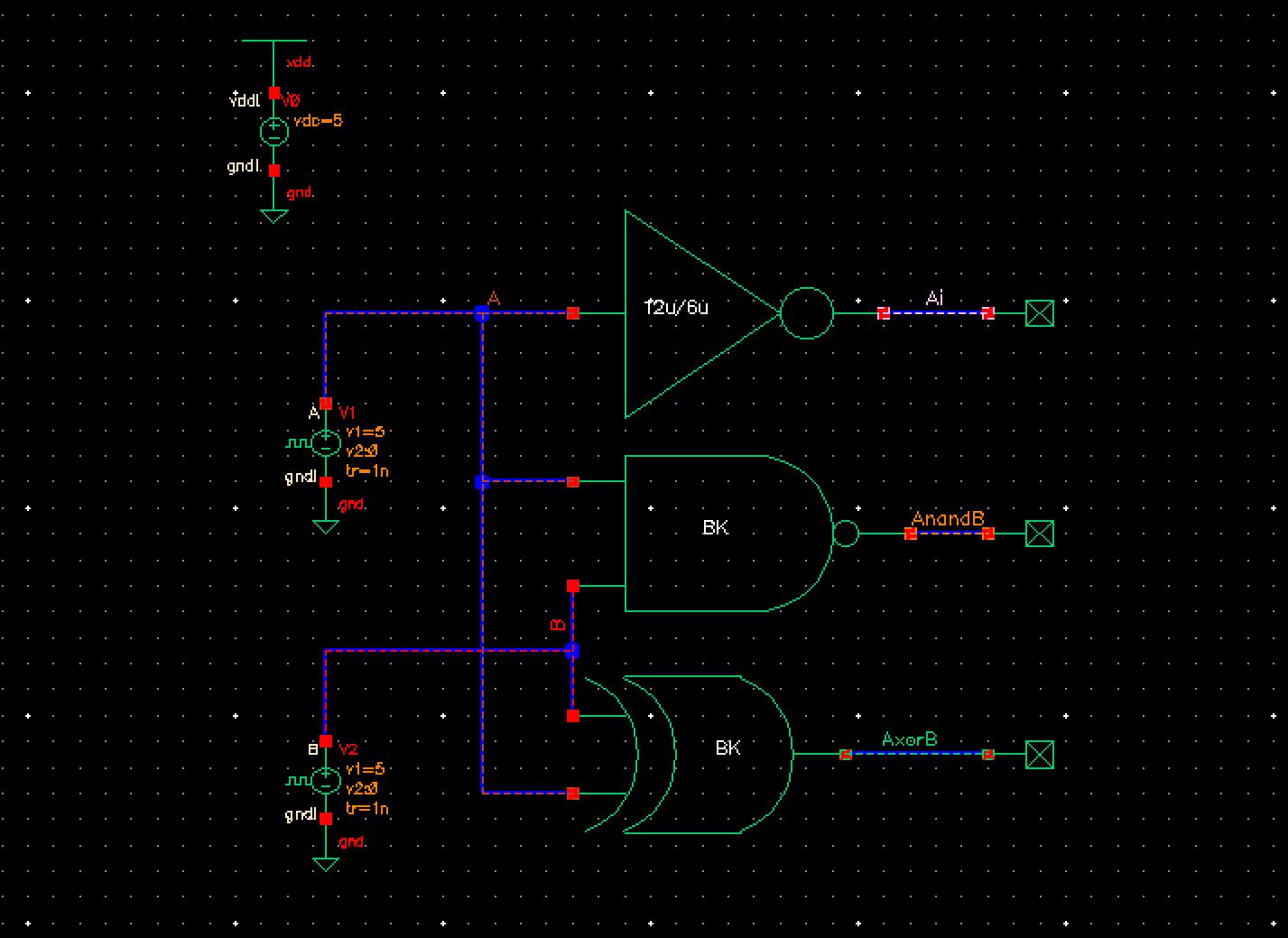
I
created a simulation schematic using three different gates Inverter,
NAND, and XOR gate with the correspoding outputs Ai, AnandB, and AxorB.
I used two different vpulse components to display the corresponding
different values with different logic inputs. Input B runs half the
period as input A. This simulation using spectre will provide the
signals: 00, 01, 10, and 11.
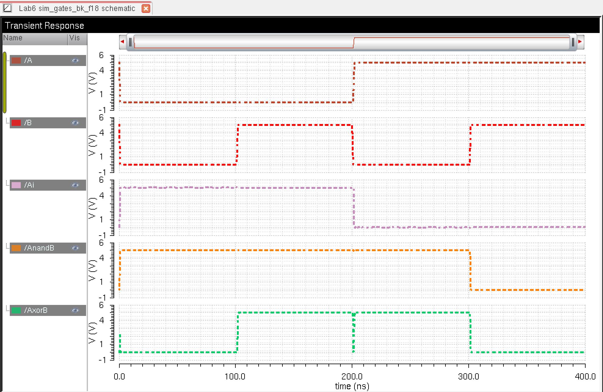
Comment about glitching:
When
the inputs transition from 01 to 10 we can see that the output of the
XOR gate "glitches" due to the rise and fall time. When the inputs are
transitioning, the XOR gate voltage tries to change simultaneously
causing that short dip at 200ns. By reducing the rise and fall time, we
can reduce the chance of this glitch.
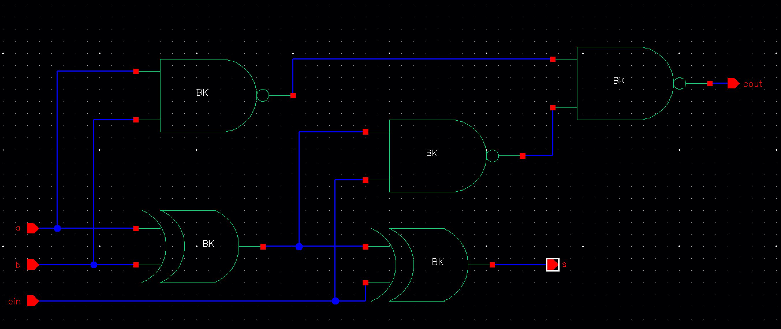
Using
the gates within this lab, a full adder is created using 3 NAND gates
and 2 XOR gates. This schematic uses three inputs a,b, and cin and uses
two outputs cout and s.
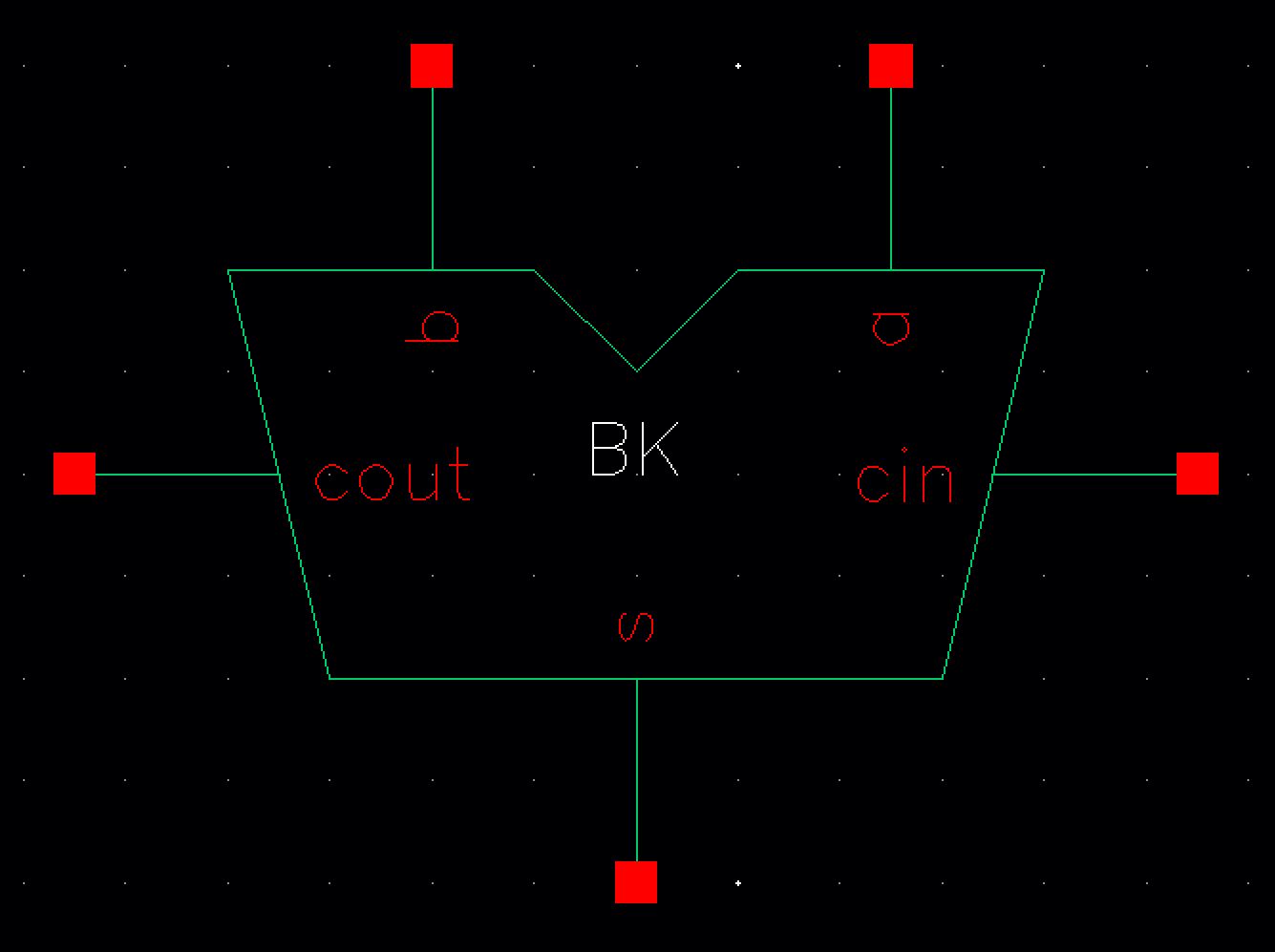
After
drafting the full adder schematic, I created the symbol above in
regards to what the symbol usually looks like on schematics for a full
adder.
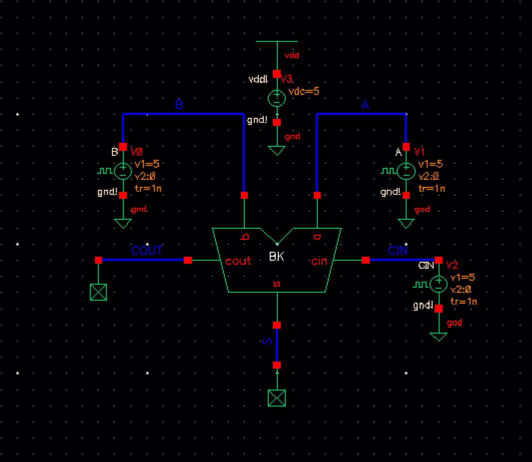
Here is the schematic implementing the full adder with three given inputs using "vpulse" to give logic inputs for the gates.
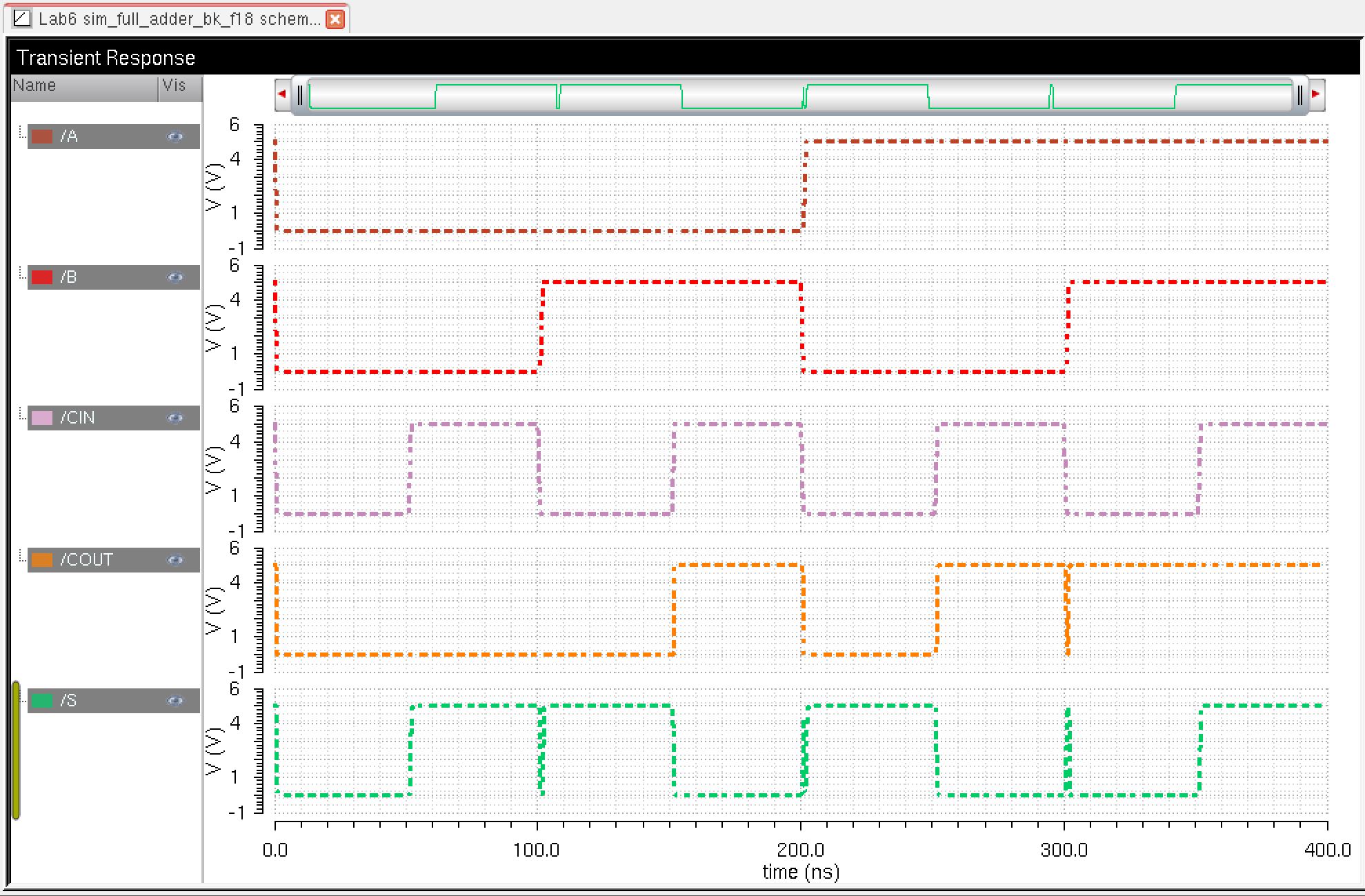
Here is the output for the drafted schematic of the full adder with the inputs: 000, 001, 010, 011, 100, 101, 110, 111
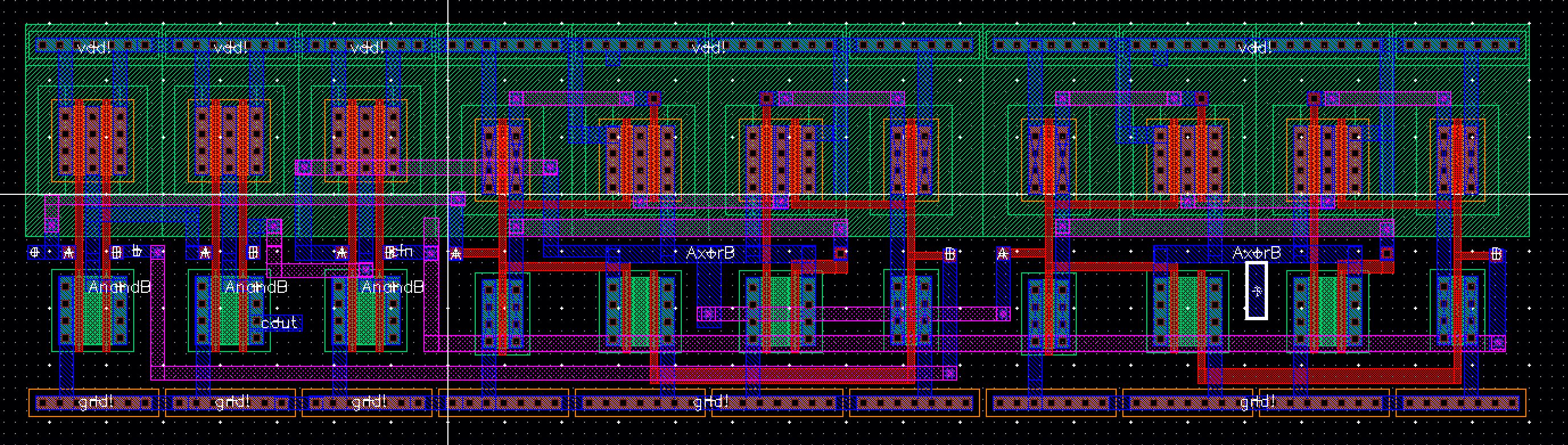
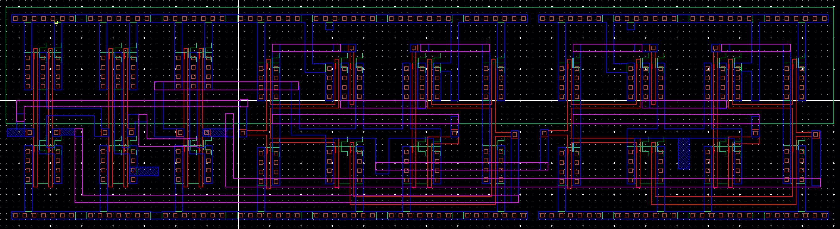
Above is the layout for the full adder, this is implemented using 5 gates
side by side with three NAND gates and 2 XOR gates from left to right.
Due to the complexity of the layout, metal2 has been used to ensure
that wires do not cross and cause problematic outcomes. Furthermore,
since these gates are laid out side by side, vdd! and gnd! can be
connected easily. Also the layout has passed the DRC verification with
no errors.
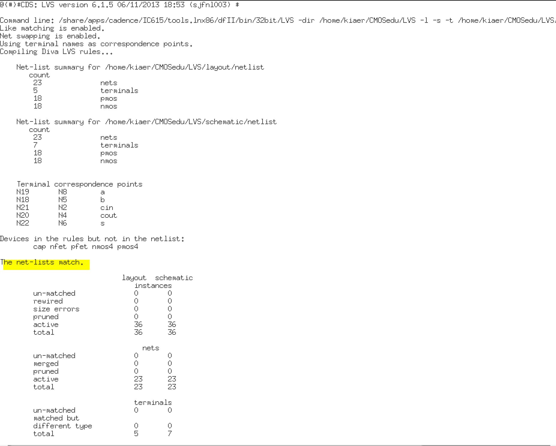
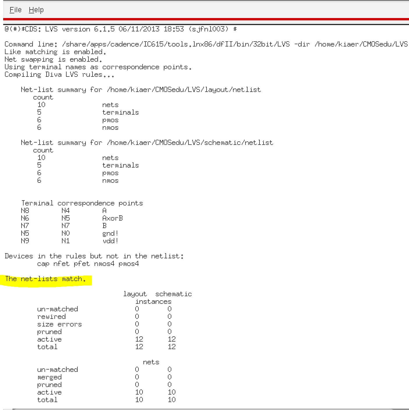
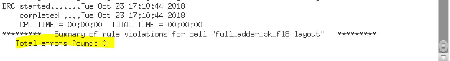
The
extracted view of the full adder and I performed the verification
test LVS to ensure that the schematic and layout (extracted) netlist
match accordingly.
After, I made sure to backup the files needed for this lab and the directory created within Cadence, which can be found here in Lab6.zip
Return to Brian's Labs