Lab 5 - ECE 421L 

Author: Brian Medrano Kiaer

Email: kiaer@unlv.nevada.edu

October 8, 2018

Prelab work: 

- Go through Tutorial 3 

http://cmosedu.com/jbaker/courses/ee421L/f18/students/kiaer/lab5/snip1.JPG

Above is the final schematic of the inverter with the input labeled as "A" and the output labeled as "Ai" using a 12u/0.6u PMOS component and a 6u/0.6u NMOS component. 

http://cmosedu.com/jbaker/courses/ee421L/f18/students/kiaer/lab5/snip2.JPG

Here is the schematic that will be used for the simulation, an inverter symbol was created for a simple way of interpreting the above schematic as an inverter. 

http://cmosedu.com/jbaker/courses/ee421L/f18/students/kiaer/lab5/snip3.JPG

Lastly, here is the output of the final schematic of the inverter. Displayed is a split graph to visually see the input and output results accordingly. The input graph (top) shows a linear increase in voltage while we can see that the output graph (bottom) will invert once met half way at the input voltage. 

Lab Work: 

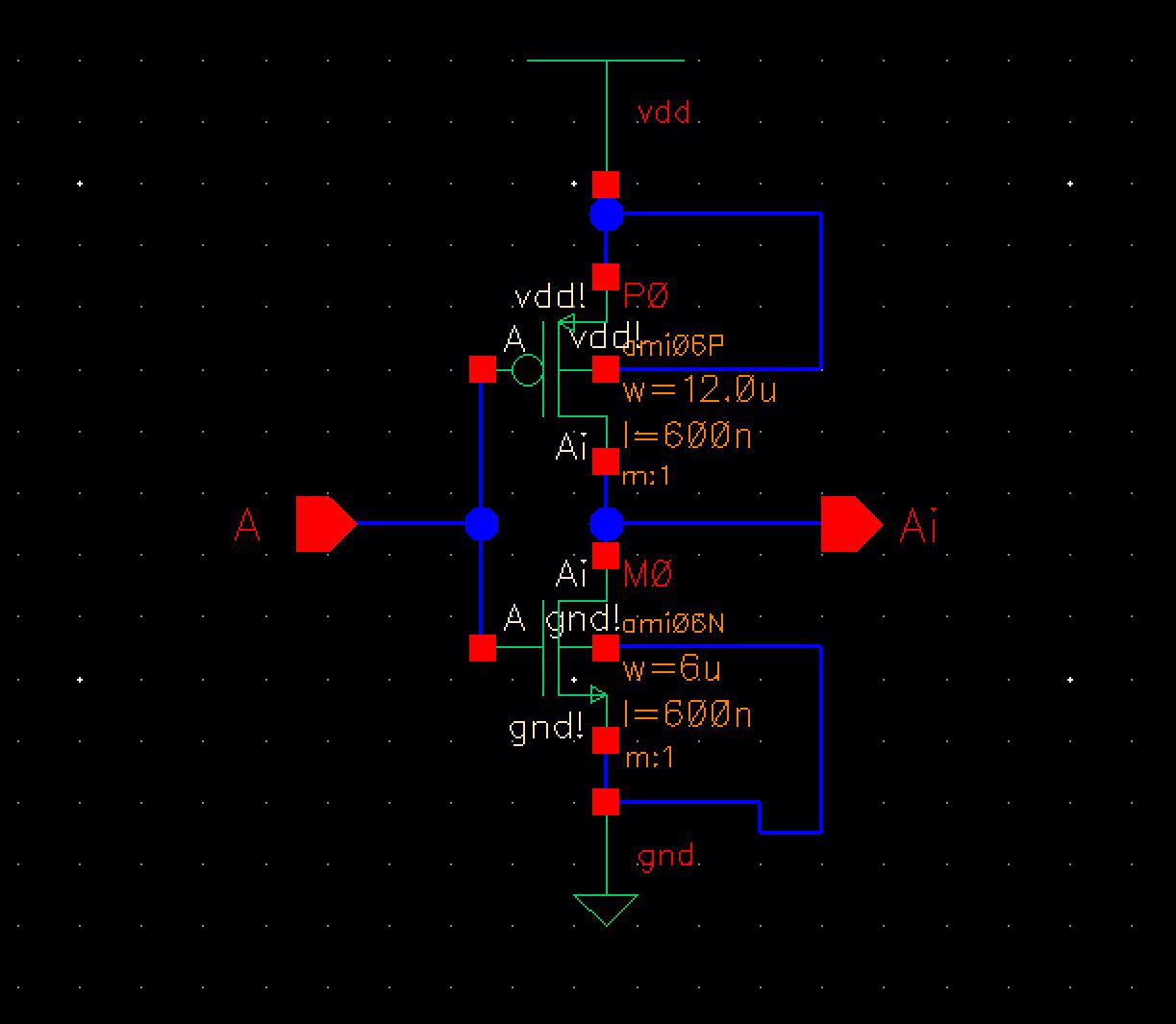
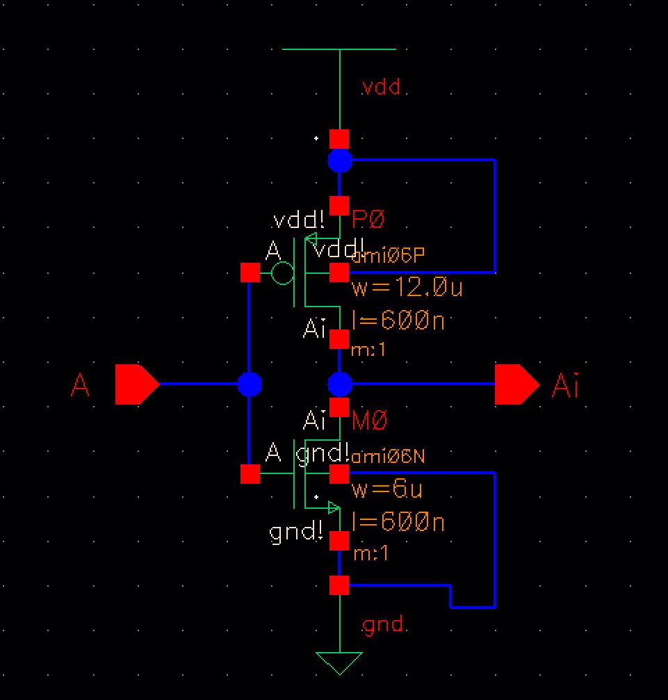
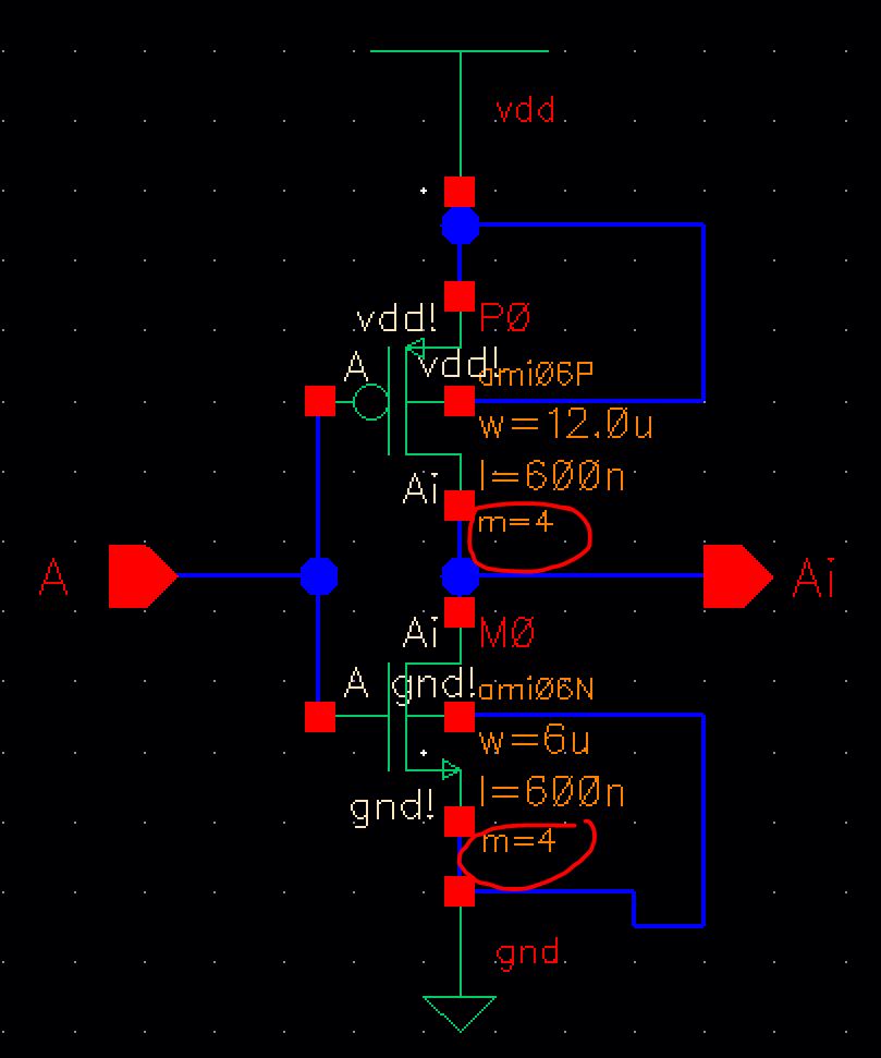
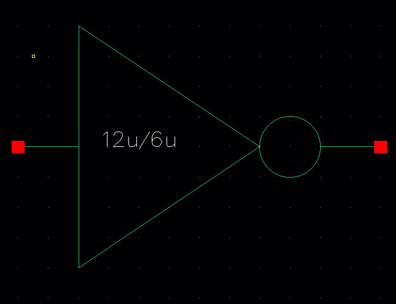
Draft schematics, layours, and symbols for two inverters having sizes of: 

    - 12u/6u (= width of the PMOS / width of the NMOS with both devices having minimum lengths of 0.6u)
    -
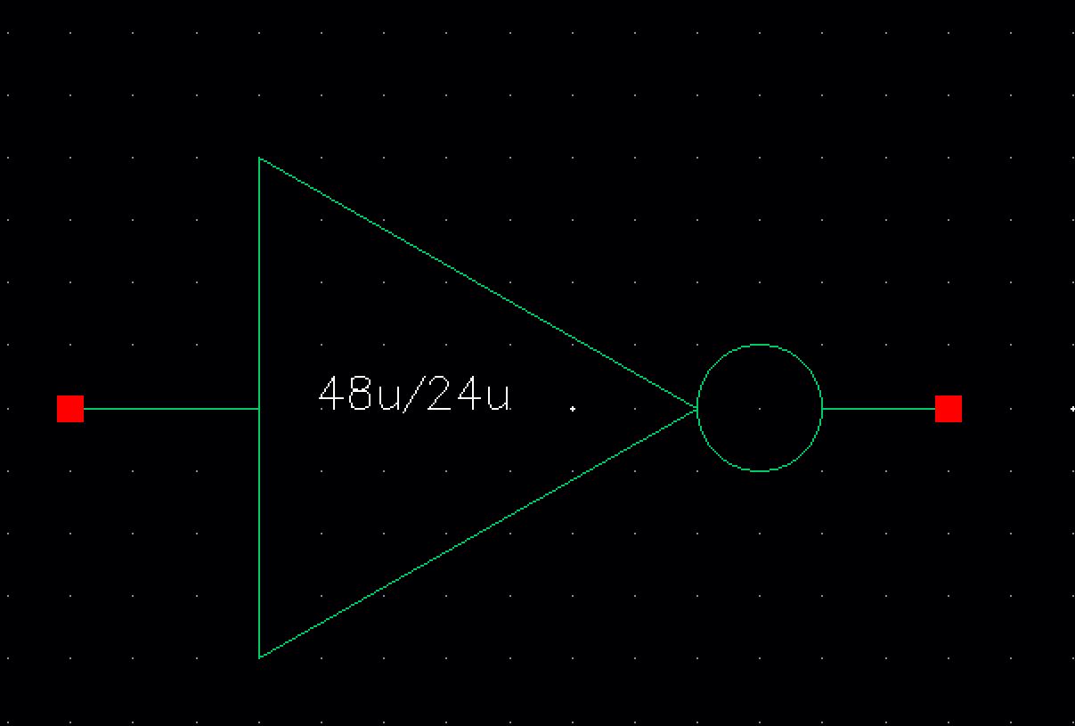
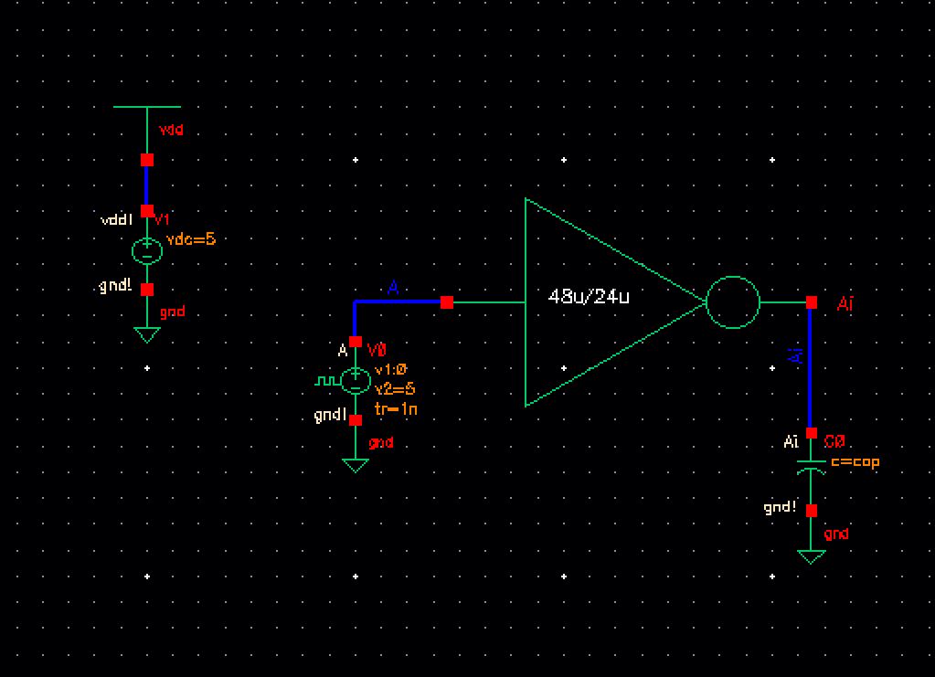
48u/24u where the devices use a multiplier, M = 4 

http://cmosedu.com/jbaker/courses/ee421L/f18/students/kiaer/lab5/snip4.JPG   http://cmosedu.com/jbaker/courses/ee421L/f18/students/kiaer/lab5/snip9.JPG

The inverter schematic with a 12u/0.6u PMOS and 6u/0.6u NMOS with m set to 1.  (Left)

The inverter schematic with a 48u/0.6u PMOS and 24u/0.6u NMOS with m set to 4. (right)

1. http://cmosedu.com/jbaker/courses/ee421L/f18/students/kiaer/lab5/snip5.JPG   2.  http://cmosedu.com/jbaker/courses/ee421L/f18/students/kiaer/lab5/snip6.JPG        3.   http://cmosedu.com/jbaker/courses/ee421L/f18/students/kiaer/lab5/snip10.JPG   4.  http://cmosedu.com/jbaker/courses/ee421L/f18/students/kiaer/lab5/snip11.JPG

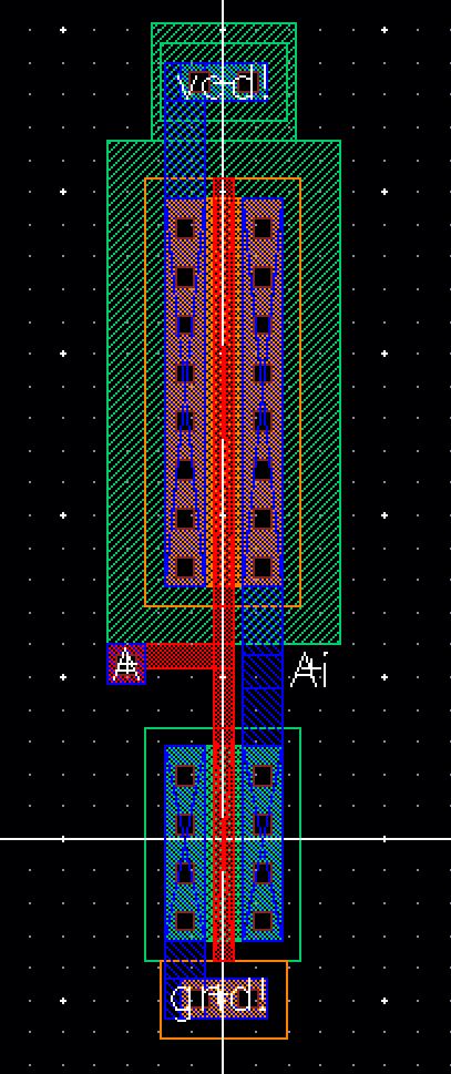
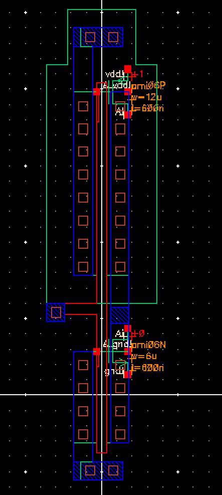
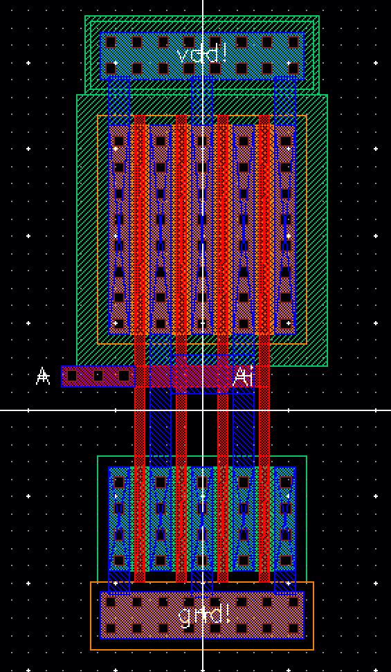
The layout for the 12u/0.6u PMOS and 6u/0.6 NMOS (1) and the layout for the 48u/0.6u PMOS and 24u/0.6 NMOS inverter (3) for the above inverter schematic. 

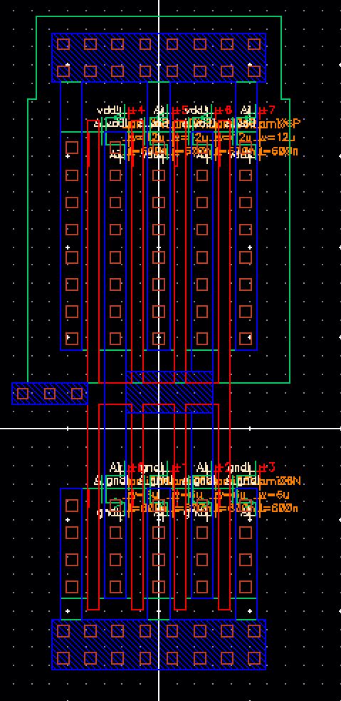
The extracted view (2 & 4) verifies the values of the PMOS and NMOS. 


http://cmosedu.com/jbaker/courses/ee421L/f18/students/kiaer/lab5/snip7.JPG   http://cmosedu.com/jbaker/courses/ee421L/f18/students/kiaer/lab5/snip12.JPG

http://cmosedu.com/jbaker/courses/ee421L/f18/students/kiaer/lab5/snip20.JPG     http://cmosedu.com/jbaker/courses/ee421L/f18/students/kiaer/lab5/snip21.JPG

I 
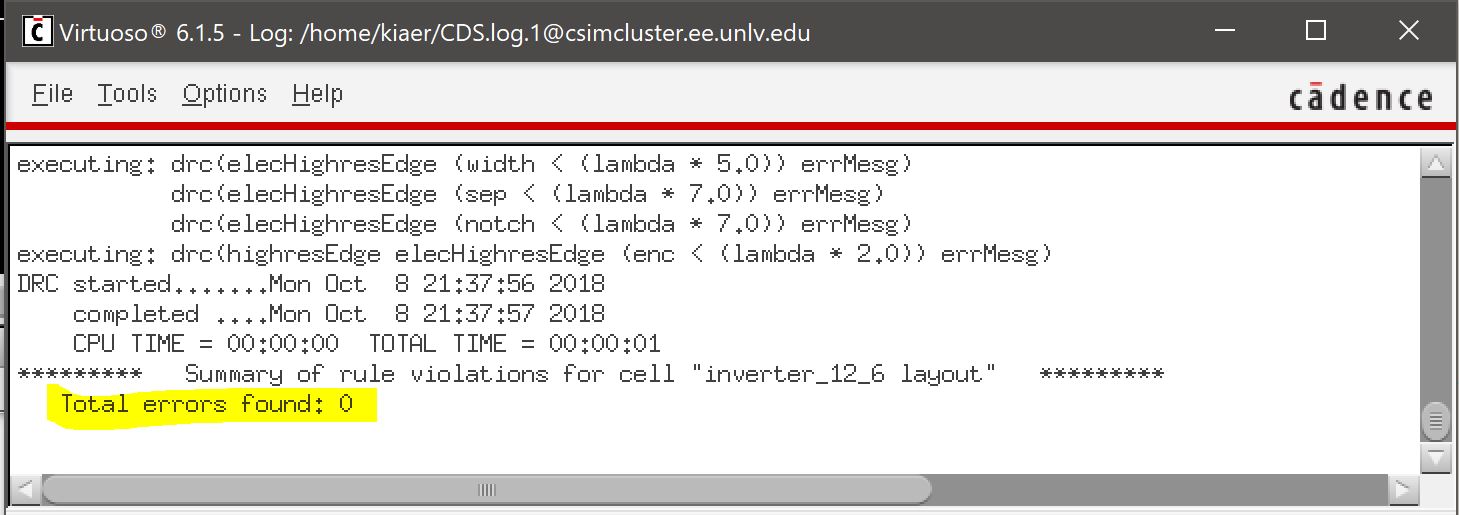
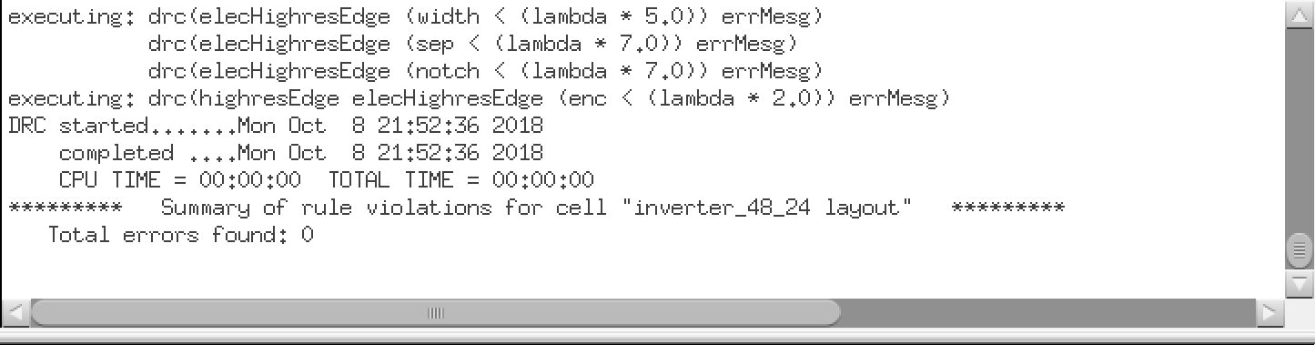
also verified through DRC to ensure there are no errors (Verify -> 
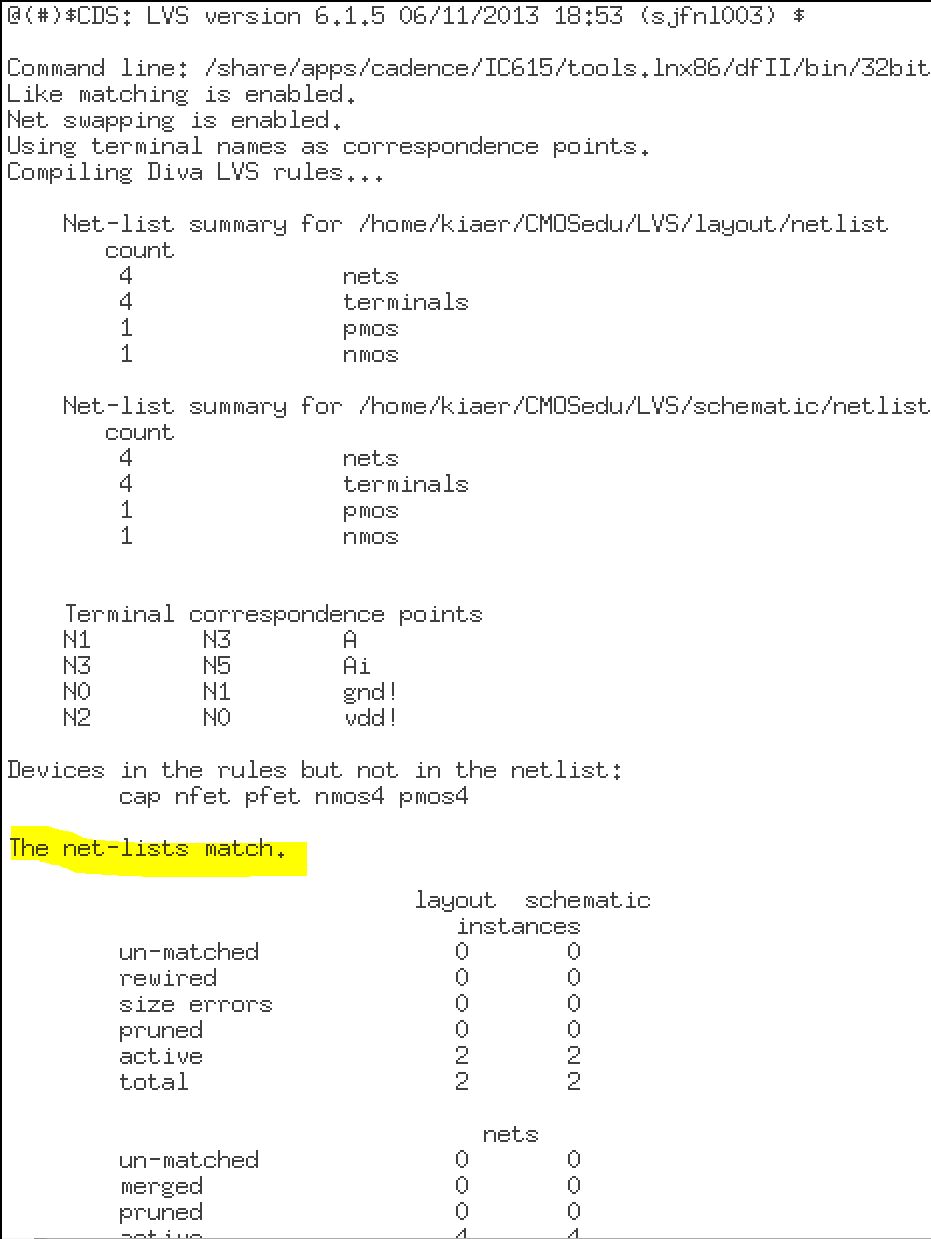
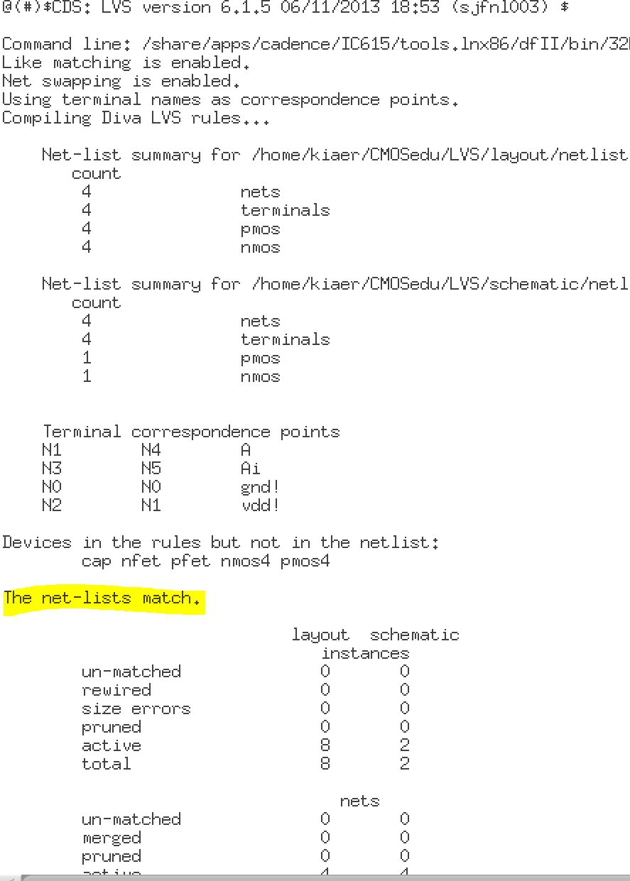
DRC) and LVS the layout too (Verify->LVS) both net-lists matched.

http://cmosedu.com/jbaker/courses/ee421L/f18/students/kiaer/lab5/snip8.JPG   http://cmosedu.com/jbaker/courses/ee421L/f18/students/kiaer/lab5/snip13.JPG

The symbol created from Create -> Cellview ->From Cellview ..

I also added the size of the PMOS/NMOS Width to ensure I do not get confused with ther other symbols. 


http://cmosedu.com/jbaker/courses/ee421L/f18/students/kiaer/lab5/snip15.JPG

Spectre simulation:
http://cmosedu.com/jbaker/courses/ee421L/f18/students/kiaer/lab5/snip14.JPG

Below is the schematic simulated using "UltraSim" also shown in the lower image beside the visualization.  

http://cmosedu.com/jbaker/courses/ee421L/f18/students/kiaer/lab5/snip16.JPG

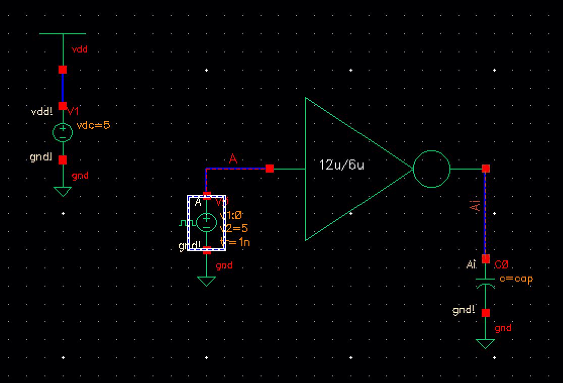
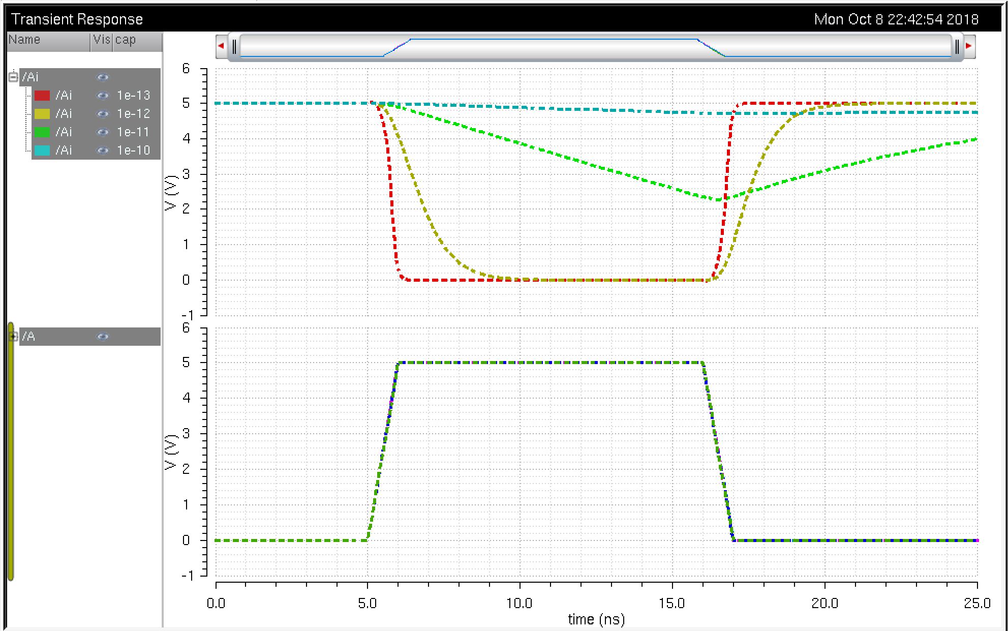
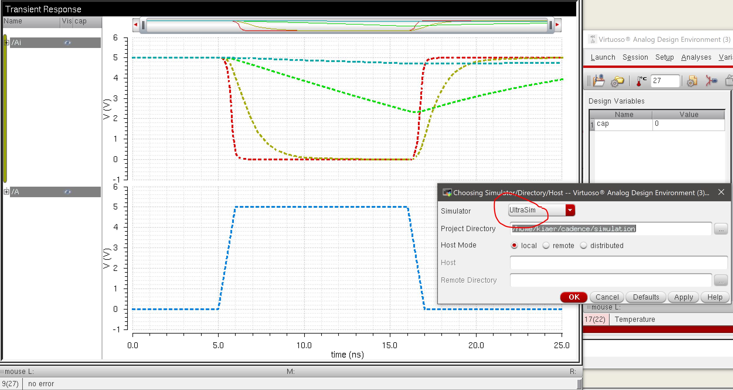
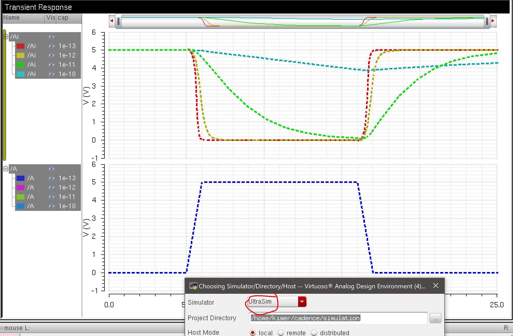
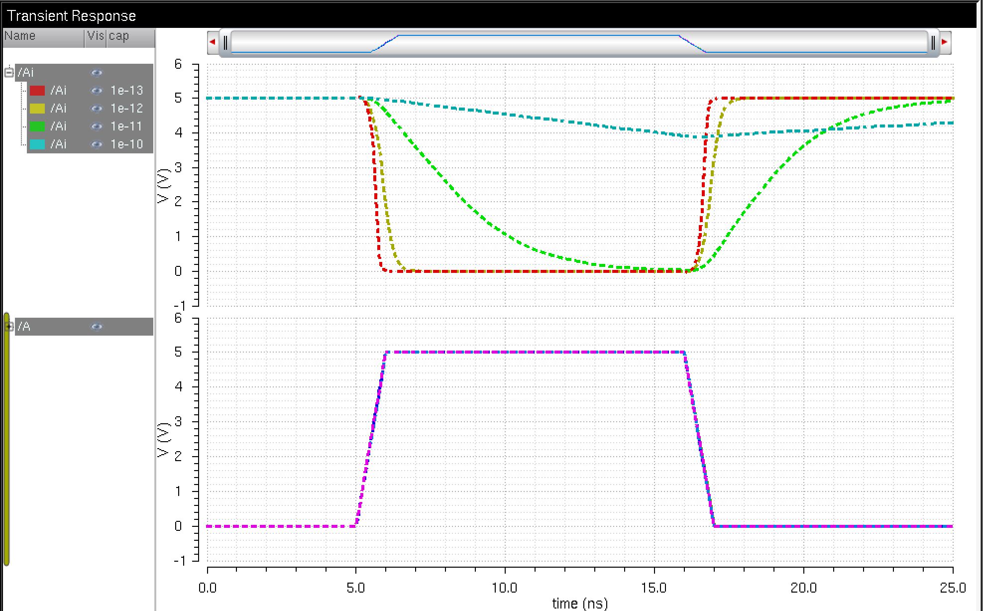
Spectre (top) and UltraSim (bottom) spiced model driving a capacitive load from 100fF, 1pF, 10pF, and 100pF. Within ADE L I created a transient response analyses for 25ns. I also created a variable called "cap" for capacitor that we can vary using parametric analysis. Within the parametric window I used the cap variable from 100fF to 100pF using the step mode = decade and assigned 1 step per decade which will be able to simulate the above visualization. It appears that the smaller the capacitive load the more inverted the output becomes. For example, the output using the 100fF (red line) inverters the input A almost perfectly. However, the larger capacitive load 100pF is straight line regardless of the input pulse. 
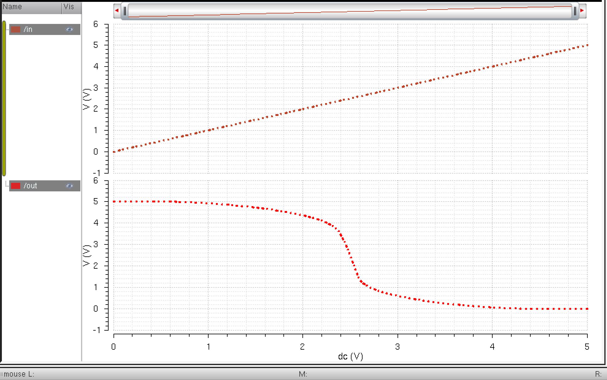


48u/24u Inverter: 


Schematic for the 48u/24u Inverter using the symbol created in the beginning of the lab.

http://cmosedu.com/jbaker/courses/ee421L/f18/students/kiaer/lab5/snip17.JPG


Below is the output "Ai" using parametric analyses of the different capacitive loads from 100fF to 100pF. We can see that it does look slightly different than the previous inverter.
The largest capacitive load 100pF does not look like a straight line like previously. We can see that it is still slightly affected from the input A and slows downward ever so slightly.

http://cmosedu.com/jbaker/courses/ee421L/f18/students/kiaer/lab5/snip18.JPG


Below is the output using the UltraSim simulator. We can see a more definitive outline of the changes in voltage; however, the overalgraph looks fairly similar to the spectre visualization.

http://cmosedu.com/jbaker/courses/ee421L/f18/students/kiaer/lab5/snip19.JPG

Return