Lab 4 - ECE 421L
Brian Medrano Kiaer
kiaer@unlv.nevada.edu
September 23, 2018
Prelab Work:
The instructions for the prelab are:
- Back-up all of your work from the lab and the course.
- Read through this lab before starting it.
- Go through Tutorial 2
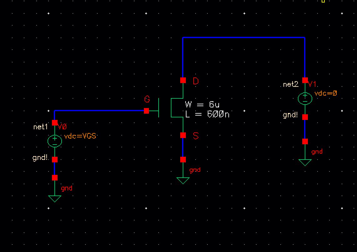
In
Tutorial 2 we were responsible for creating the schematic above. The
schematic above uses a symbol that we previously created in the
tutorial as a 6um by 600nm NMOS symbol.
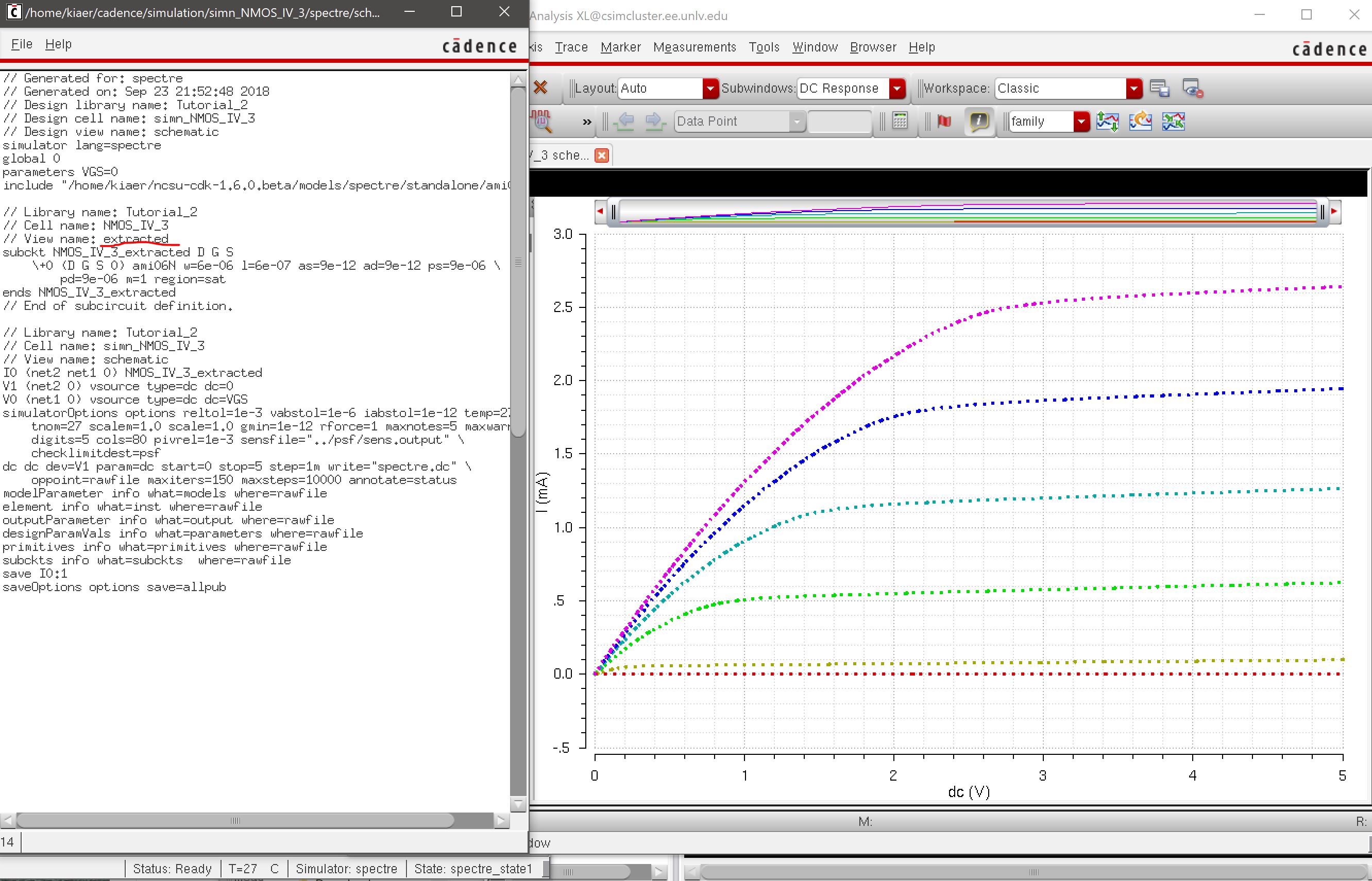
Once
the layout of the 6um by 600nm NMOS has been completed it must get
extracted (Verify->Extracted). Once that has been completed the next
step is to follow a parametric analyses. We can see the parametric
analyses on the right side of the above image and to ensure that it has
used the extracted cell the left side of the image shows the Netlist
stating it has used the extracted cell in the parametric analyses.
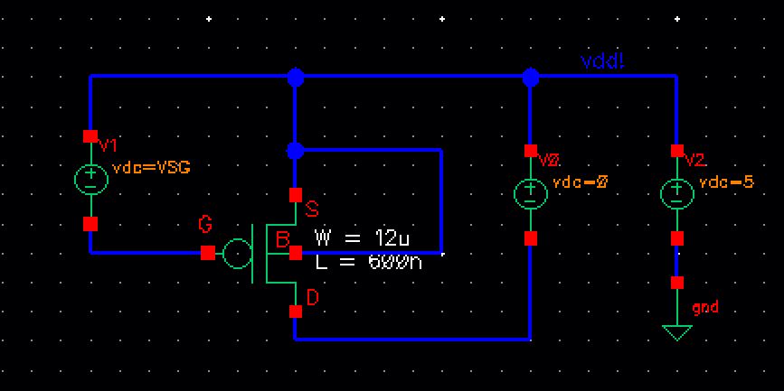
Next
is to create the schematic above but using a 12um by 600nm PMOS. The
schematic above uses a symbol that I created with a 4 terminal PMOS.
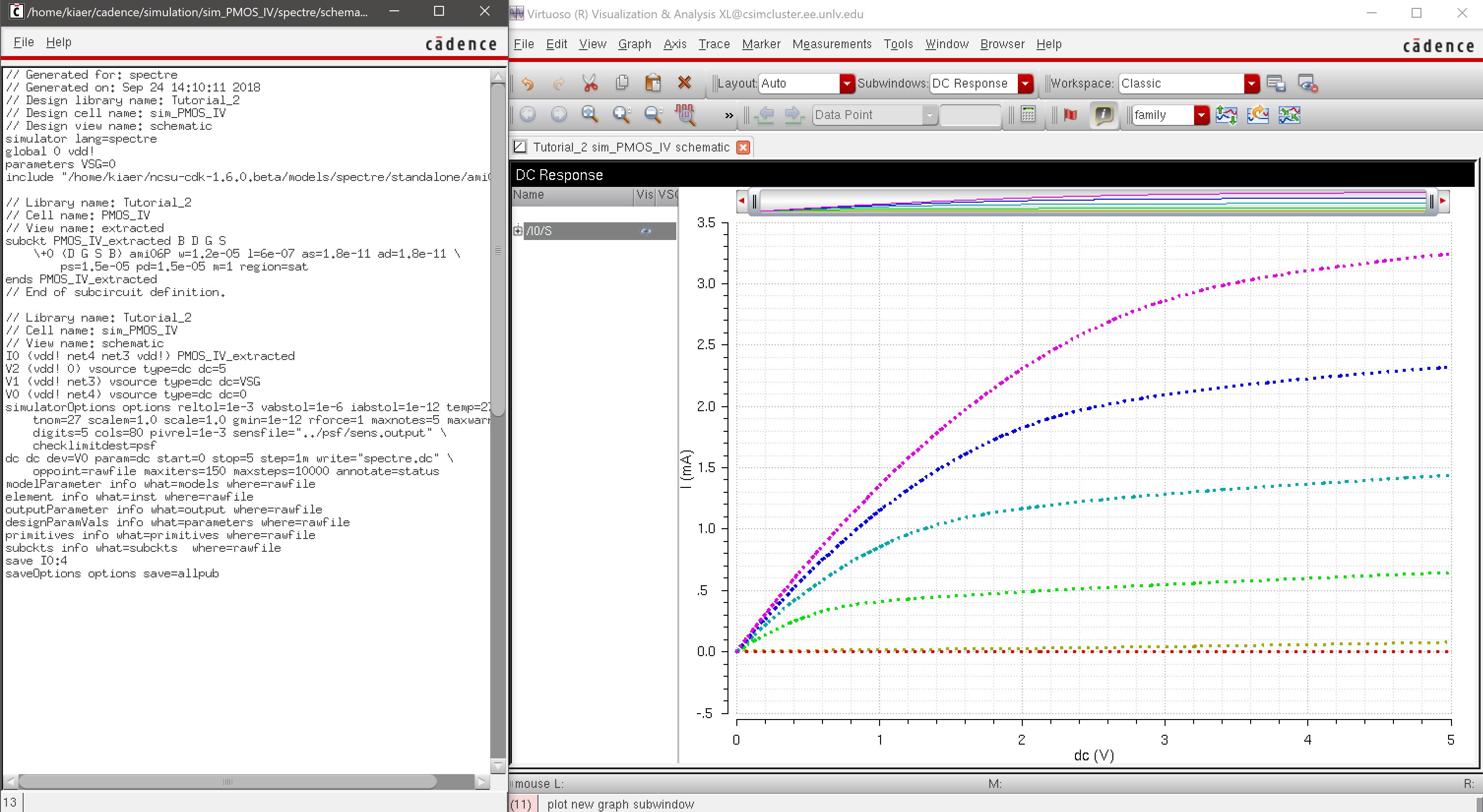
Above
is the output of the schematic using a parametric analyses of VSG. On
the left side of the image next to "View name:" states that the
simulation used the extracted cell view.
Lab
description:
- Generate 4 schematics and simulations
- A schematic for simulating ID
v. VDS of an NMOS device for VGS varying from 0 to 5 V in 1 V steps
while VDS varies from 0 to 5 V in 1 mV steps. Use a 6u/600n
width-to-length ratio.
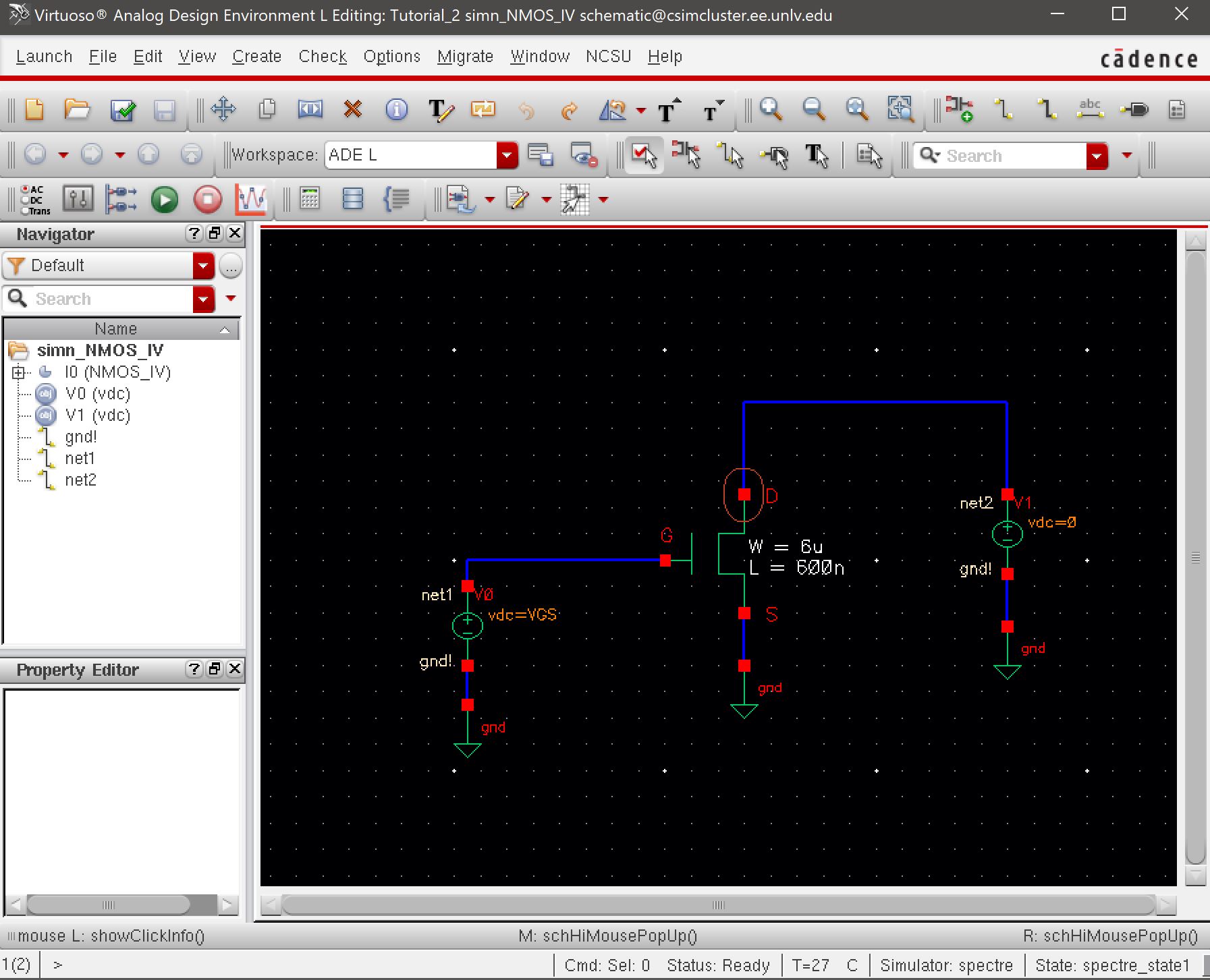
Above is a schematic that implements a NMOS component that uses a 6u/600n width-to-length ratio.
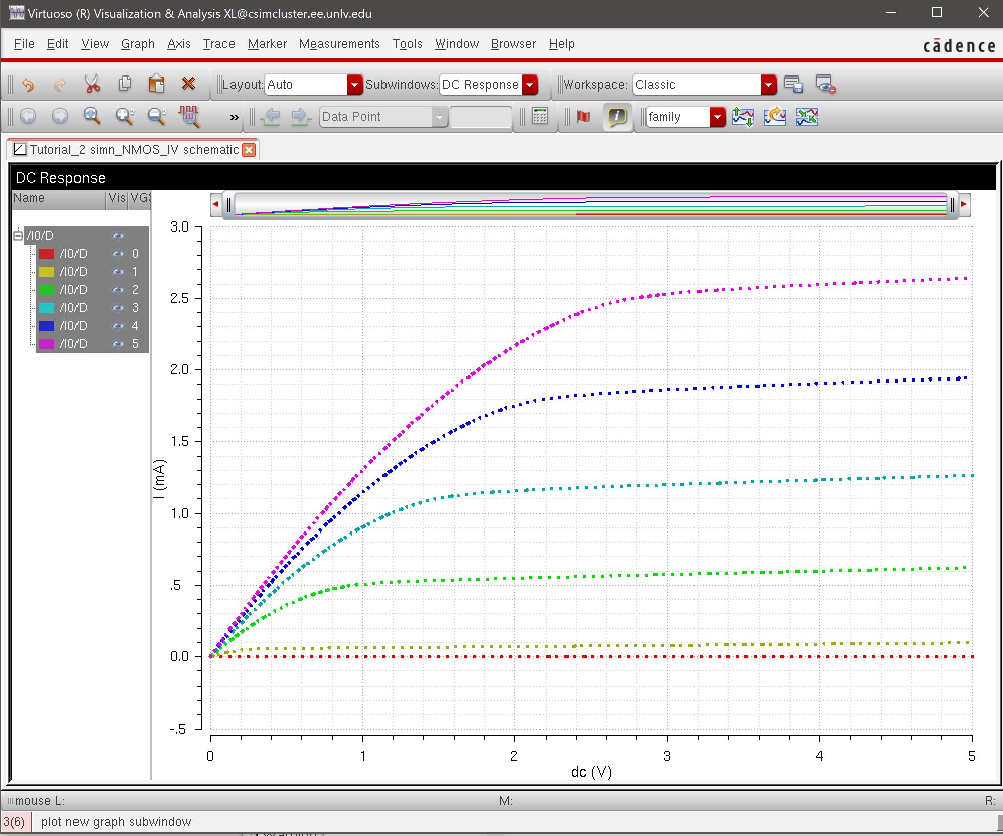
Above is the output for the first schematic showing a relation between VGS
varying from 0 to 5 V in 1 V steps while VDS varies from 0 to 5 V in 1
mV steps. In the ADE window a dc analysis has been created for /V1
which would be VDS. For a varying VGS, a parametric analysis has been
created under Tools -> Parametric Analysis
- A
schematic for simulating ID v. VGS of an NMOS device for VDS = 100 mV
where VGS varies from 0 to 2 V in 1 mV steps. Again use a 6u/600n
width-to-length ratio.
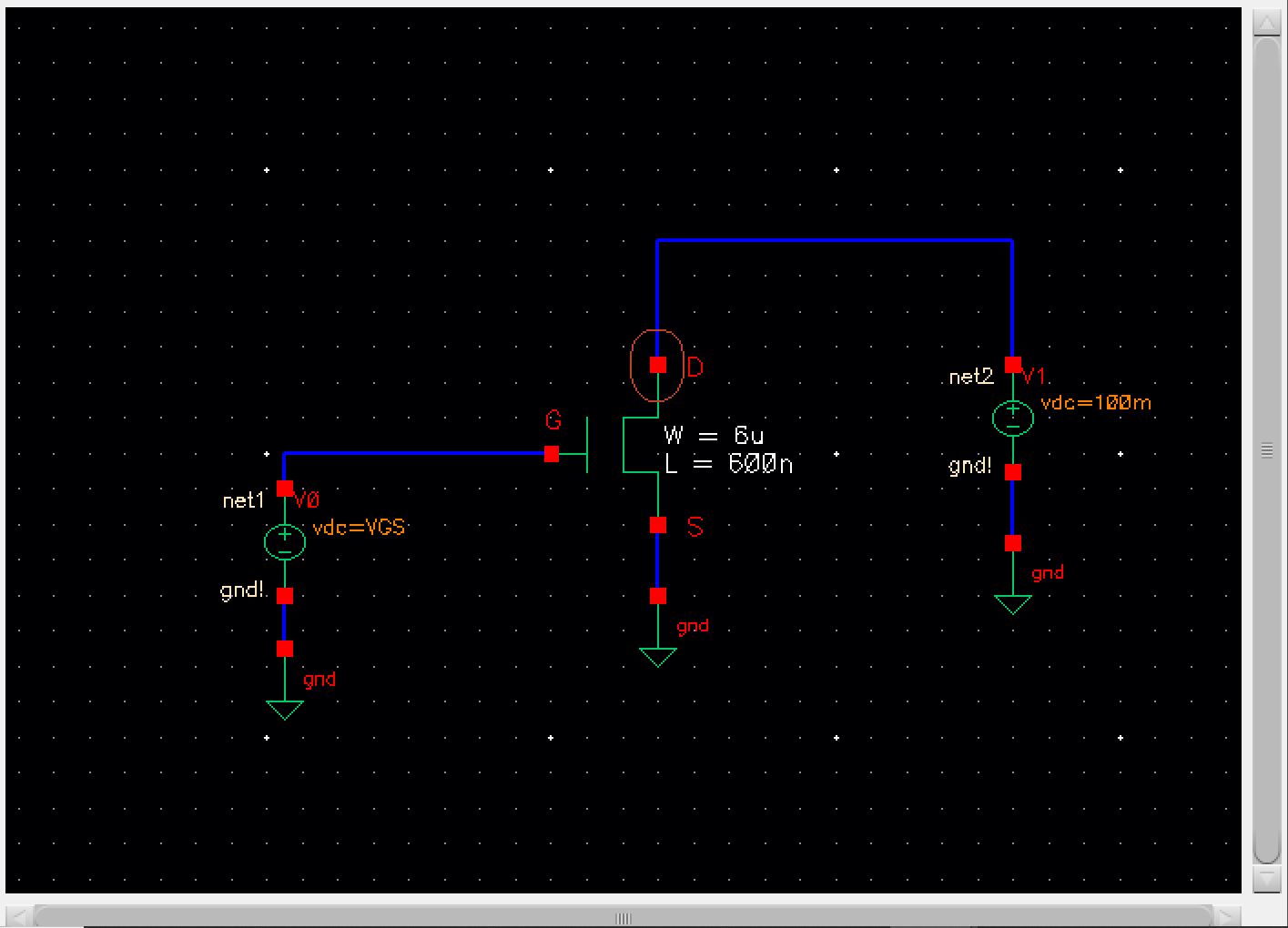
This schematic implements a NMOS with 6u/600n width-to-length ratio. VDS (V1) has a DC value of 100mV.
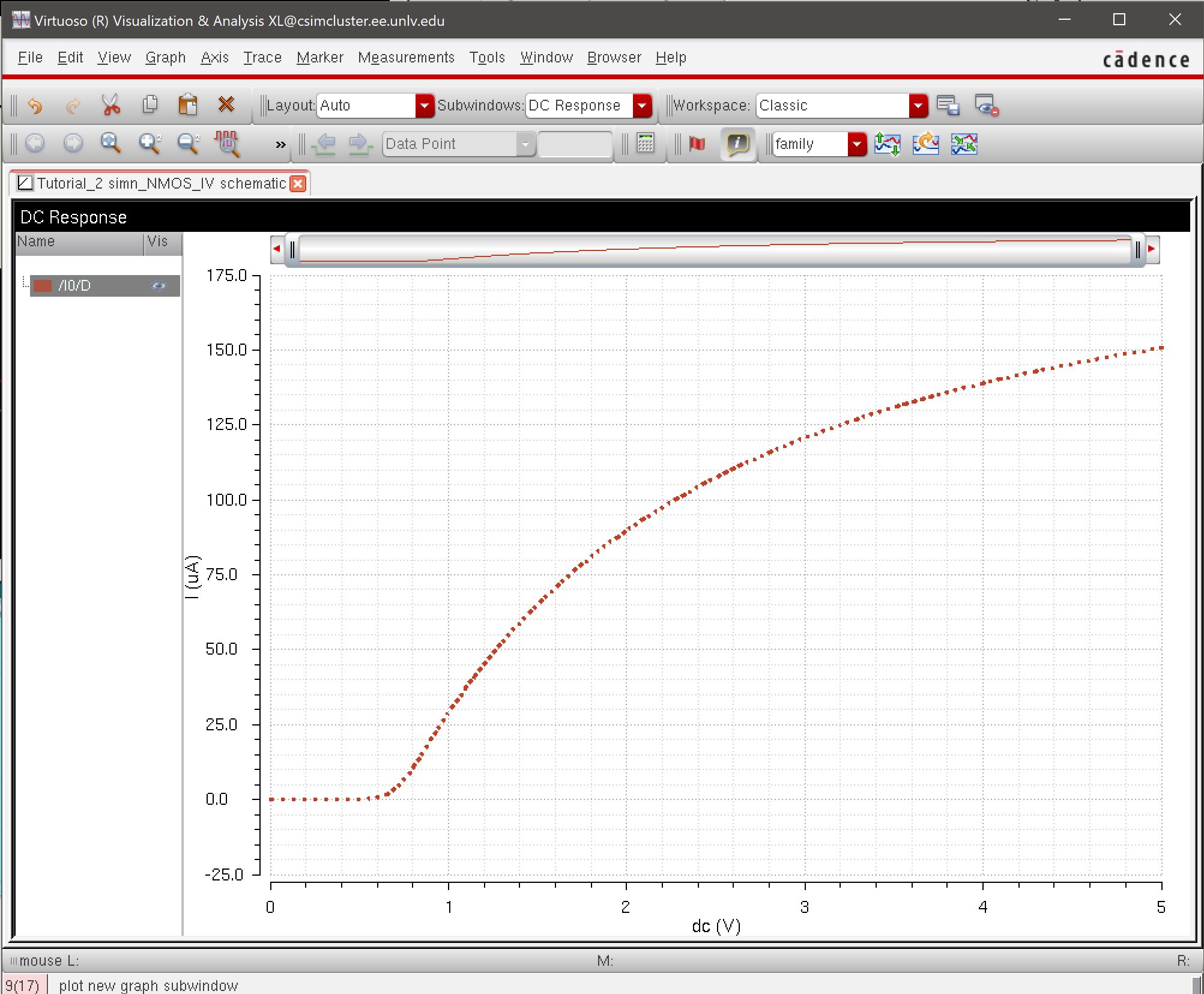
Above
is the output of the previous NMOS (6u/600n) schematic with VDS at
100mV and a varying VGS voltage from 0 to 2V in 1mV steps. Within the
ADE L, a DC Analysis was created for VGS (V0) to vary the voltage in
linear steps. VDS stays constant.
- A
schematic for simulating ID v. VSD (note VSD not VDS) of a PMOS device
for VSG (not VGS) varying from 0 to 5 V in 1 V steps while VSD varies
from 0 to 5 V in 1 mV steps. Use a 12u/600n width-to-length ratio.
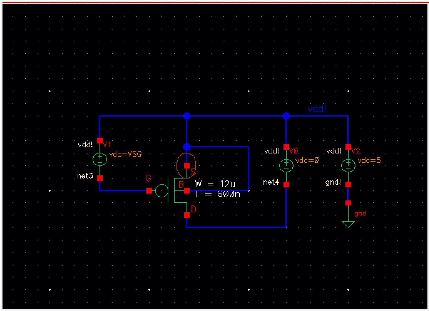
This
schematic is similar to the PMOS schematic created within the second
Tutorial. The schematic uses a 12u/600n width-to-length ratio PMOS.
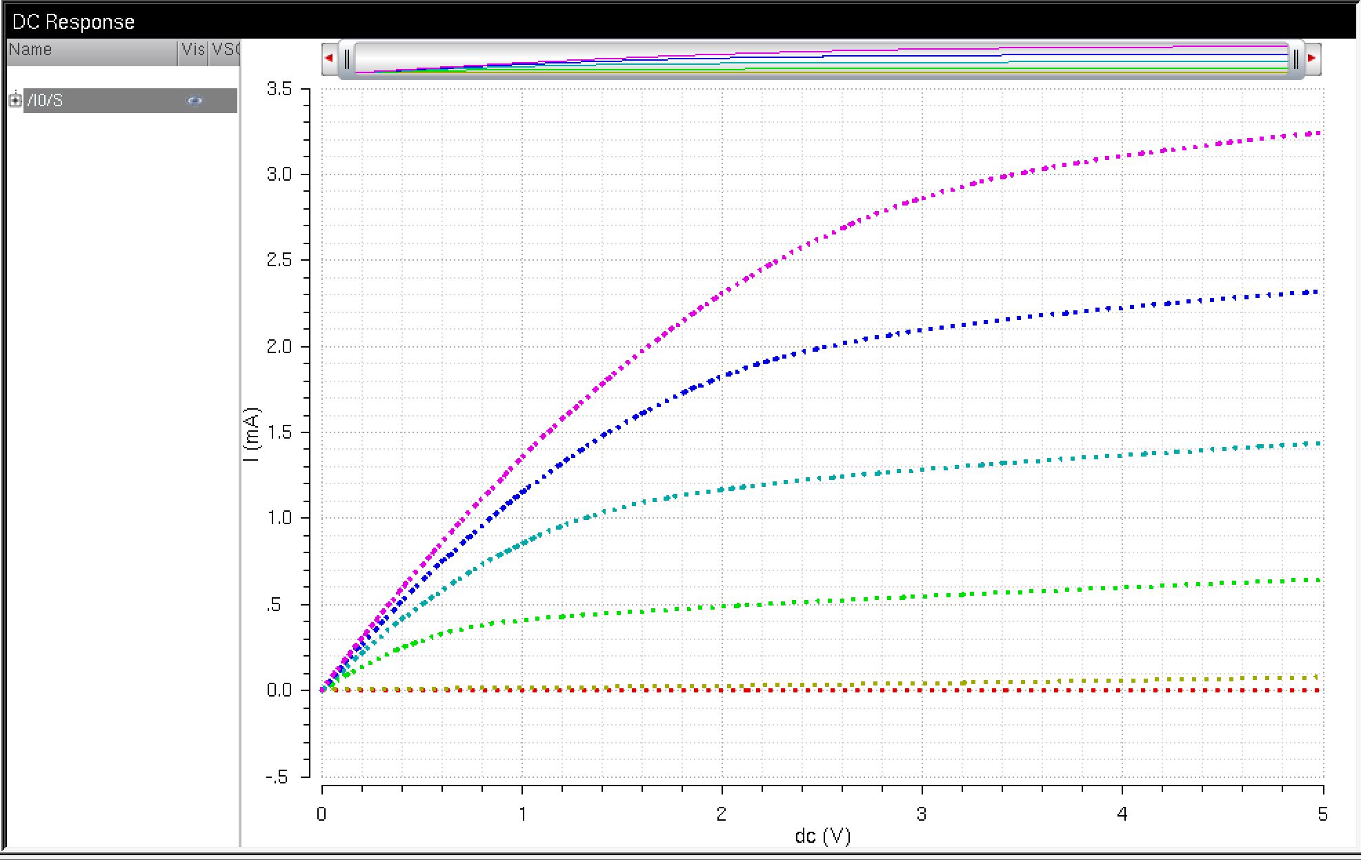
The
output of ID v. VSD with VSG varying from 0 to 5 V in 1V steps by
implementing a parametric analysis and the voltage VSD varying from 0
to 5V in 1mV steps using dc analysis for a 12u/600n width-to-ratio PMOS
component.
- A
schematic for simulating ID v. VSG of a PMOS device for VSD = 100 mV
where VSG varies from 0 to 2 V in 1 mV steps. Again, use a 12u/600n
width-to-length ratio.
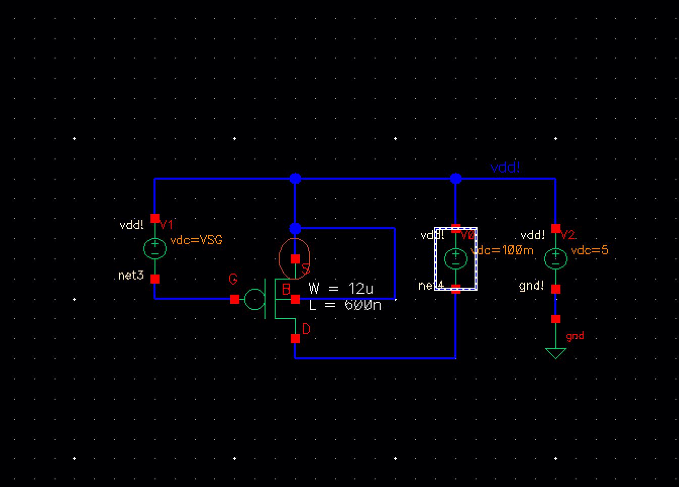
Here I set VSD(V0) = 100mV for a 12u/600n PMOS component.
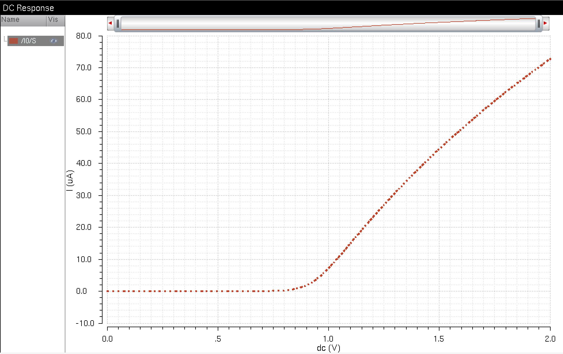
Here
is the output for the last PMOS schematic where VSD was set to 100mV.
Within the ADE, VSG's values were set by a DC analysis where VSG varies
from 0 to 2V in 1mV steps. The PMOS ratio is the same at 12u/600n
width-to-length ratio.
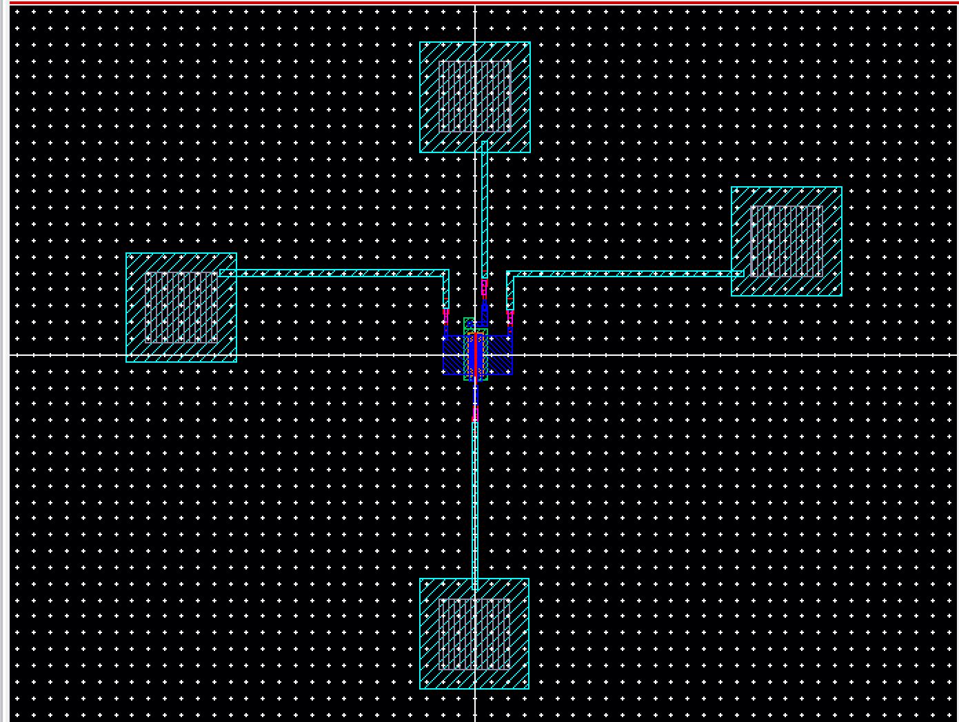
- Lay out a 6u/0.6u NMOS device and connect all 4 MOSFET terminals to probe pads
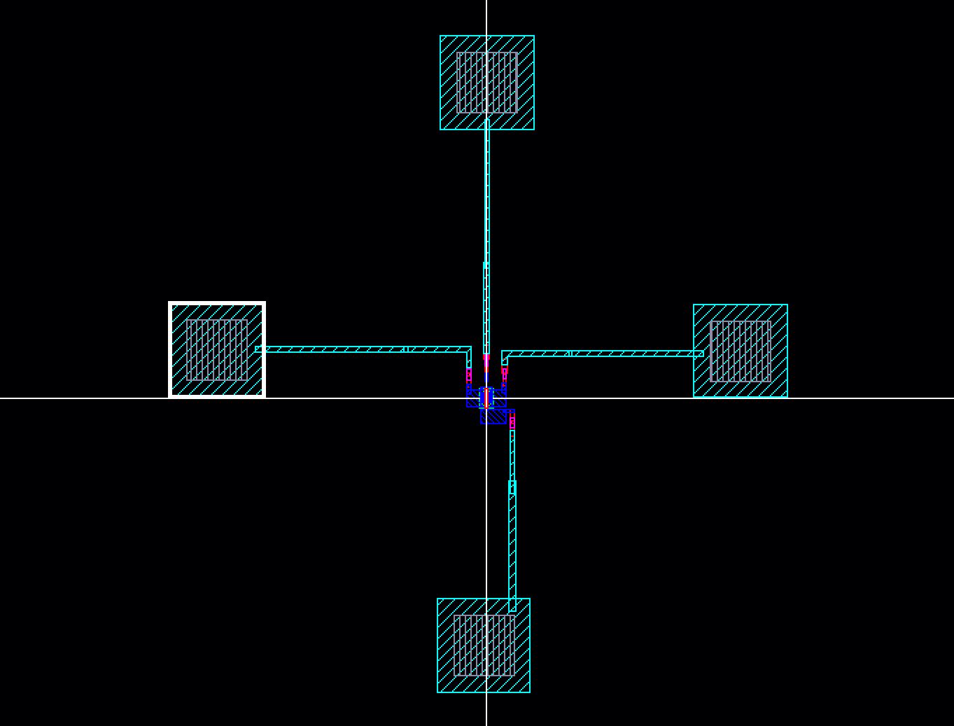
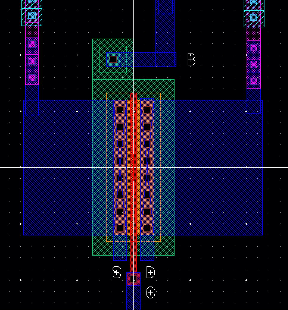
Above is the layout of a 6u/0.6u NMOS component with all 4 terminals connected to probe pads.
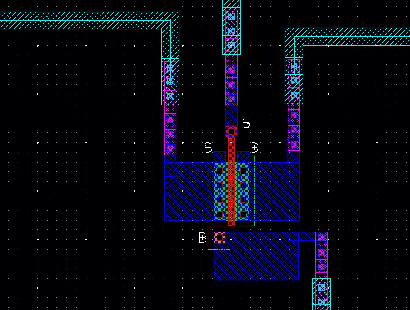
First I created the NMOS by using the "nmos" layout from the NCSU_TechLib_ami06
library. Then added the ptap layout as the "B" pin of the NMOS and the
m1_poly layout connected to the poly1 on the NMOS. Next I added metal1
layer pads connected to the 4 terminal pins S, D, G, B. Those 4 metal1
pads were connected using the m2_m1 layouts from the NCSU_TechLib_ami06
library, then metal 2 was connected to metal 3 using the "m3_m2"
layout. Lastly, a metal 3 rectangle/path was used to attach to the
probe pads.
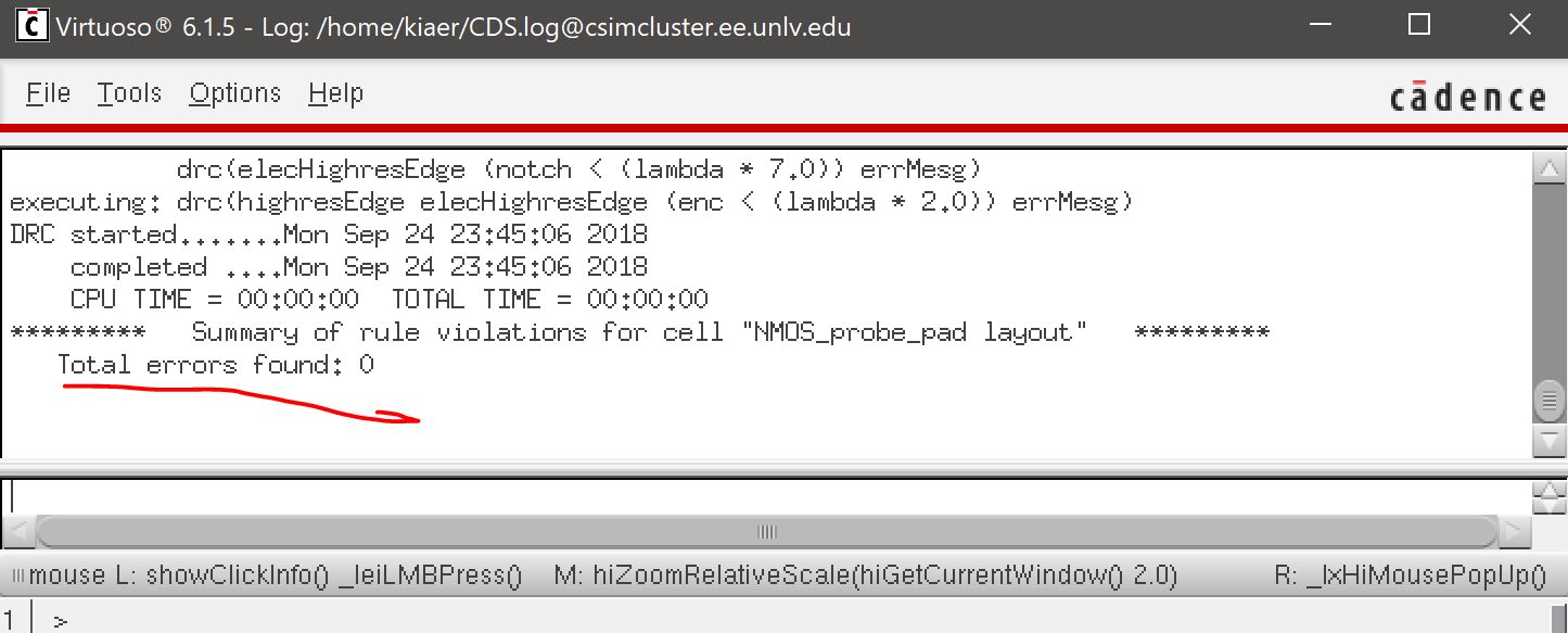
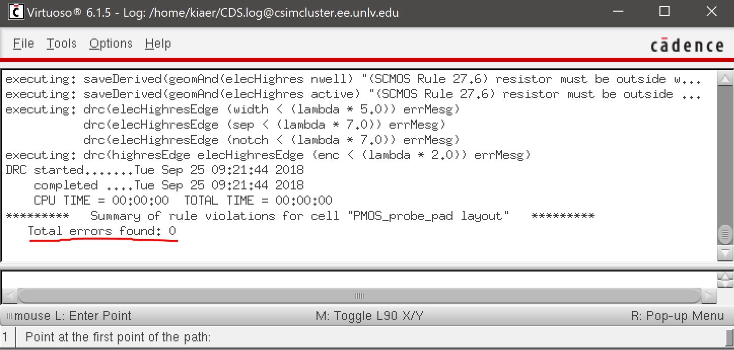
I
then used Verify->DRC to ensure that there are no errors found with
my layout. Originally, I did not provide enough space in between the
probe pads and needed a distance over 30um.
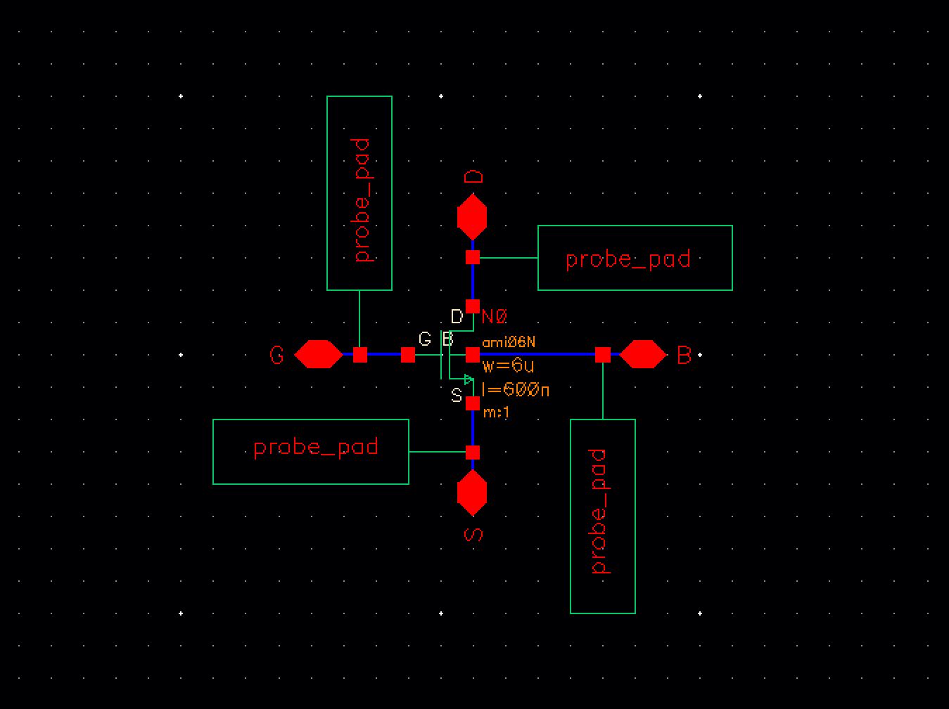
I
created the schematic to match the layout in order to perform an LVS. I
added the "nmos4" from the NSCU_Analog_Parts and then added 4
inputOutput pins onto the S, D, G, and B points. I also set the
perameters of the NMOS to be 6u/.6u width-to-length ratio. Lastly, I added 4 probe_pads onto each seperate wire.
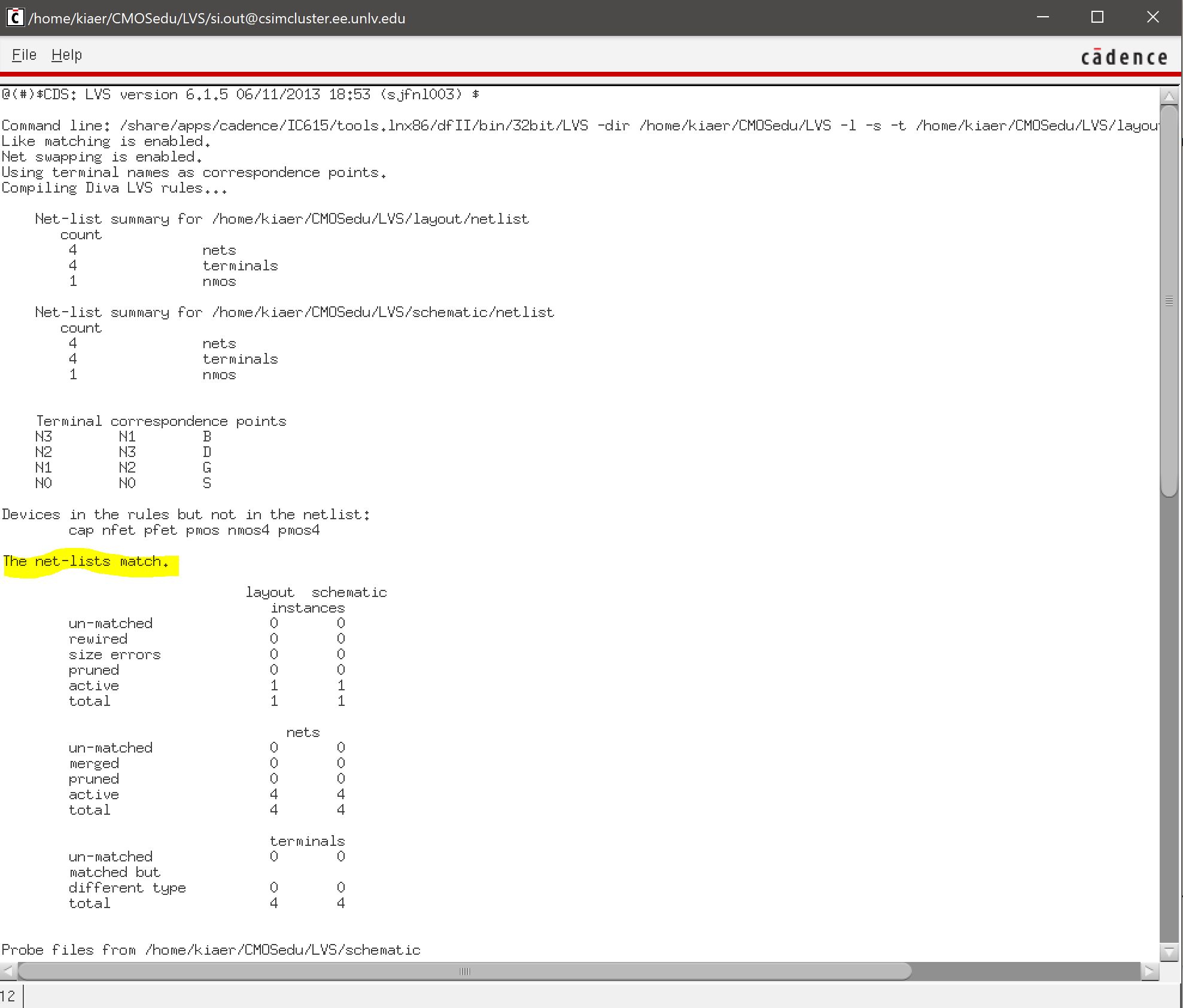
The LVS has been perfomed (Verify->LVS), the output verifies that the netlists match and the LVS is successful.
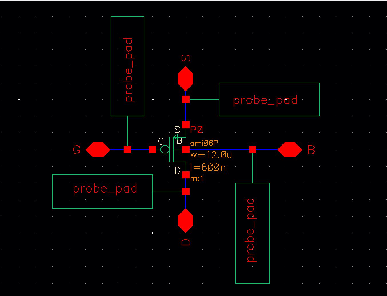
- Lay out a 12u/0.6u PMOS device and connect all 4 MOSFET terminals to probe pads.
Here
is the whole layout for a 12u/0.6u PMOS with all four terminals
(S,D,B,G) connected to probe pads. I created a metal1 pad connected to
the 4 terminals using the Rectangle/pin functions in Cadence. Then I
connected the "m2_m1" layout from the NCSU_TechLib_ami06 library to
those metal1 rectangles. After that I connected the metal2 connectors
to the "m3_m2" layout also from the same library. Lastly, I used the
path function to connect the m3_m2 layout to the probe pads using the
metal3 layer.
Finally,
I made sure to DRC (Verify->DRC) the layout to ensure that there are
no errors within the layout and the components are spaced
appropriately.
Here is the relating schematic of a 12u/600n width-to-length ratio PMOS with the 4 terminals connected to probe pads.
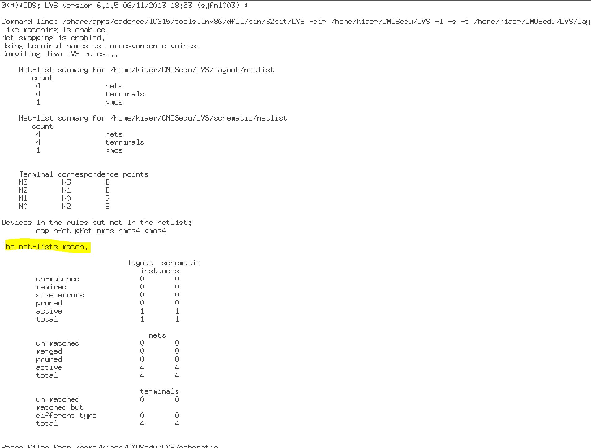
Finally,
to ensure that the layout and schematic are concise LVS needs to be
successful. Above is the output of the LVS test (Verify->LVS) and we
can see that the net lists match which is what we are looking for.
Return to Labs