Lab 2 - ECE 421L
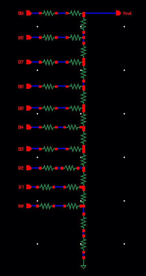
After understanding how the schematic works I went to Launch -> ADE L then in the ADE L Window pressed on Session -> Load State ->Cellview -> *Enter Key* and this is the output of the provided example schematic:
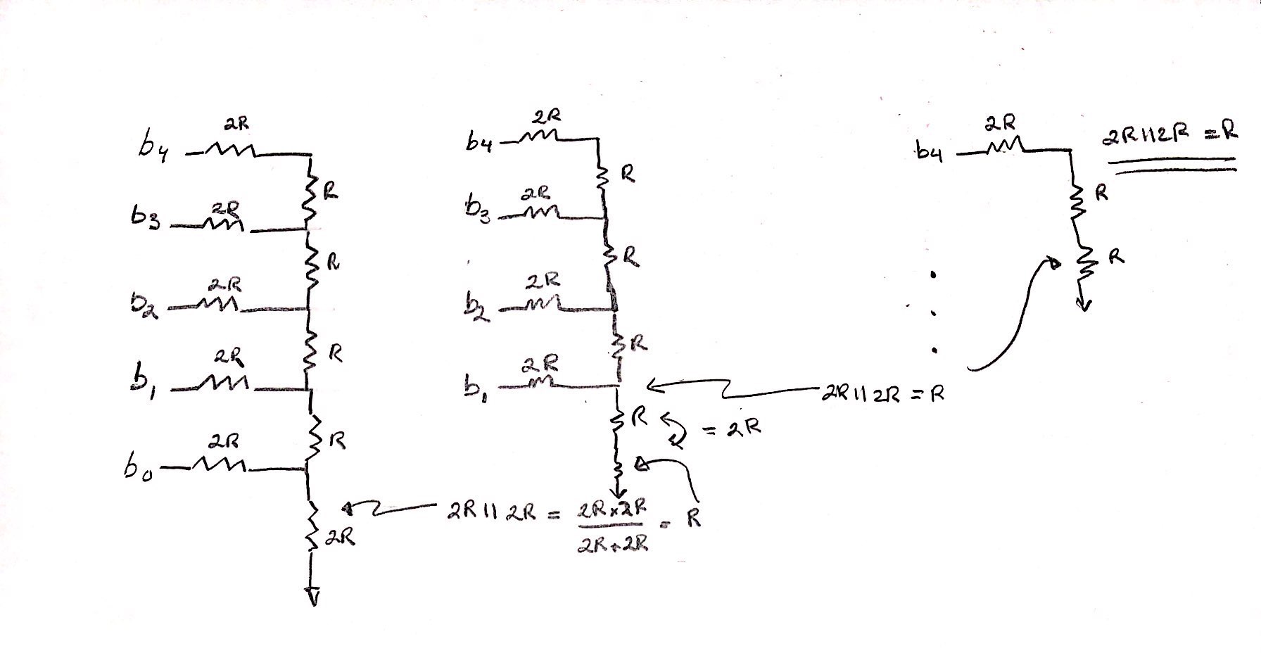
The way to find out the output resistance is by combining the resistors that are in series or that are parallel from each other, here is a 5-bit example below:
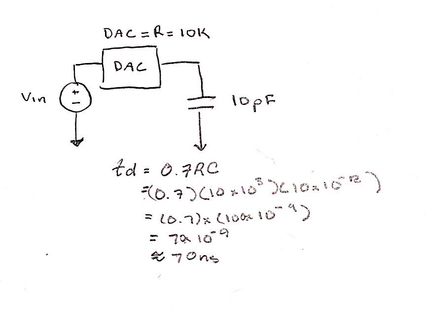
- Delay, driving a load
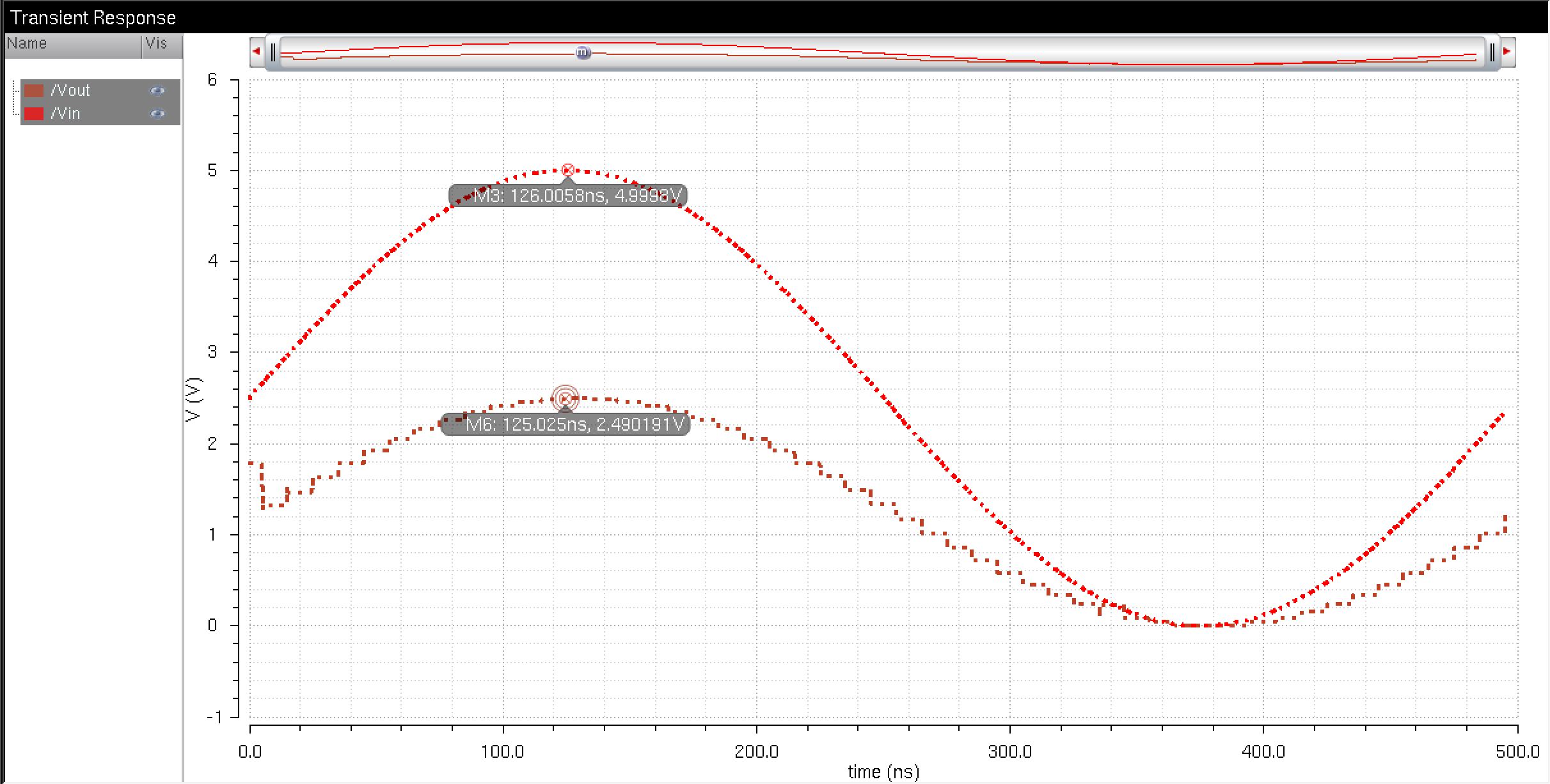
When all the DAC inputs are grounded except B9, we are able to find the output resistance as calculated above at R = 10k. When driving a load that is 10pF we are able to use the formula td = 0.7RC. Below the calculations have provided to conclude approximately 70 nanoseconds.
Here is the output of the RC Circuit using a .tran simulation at 2us.
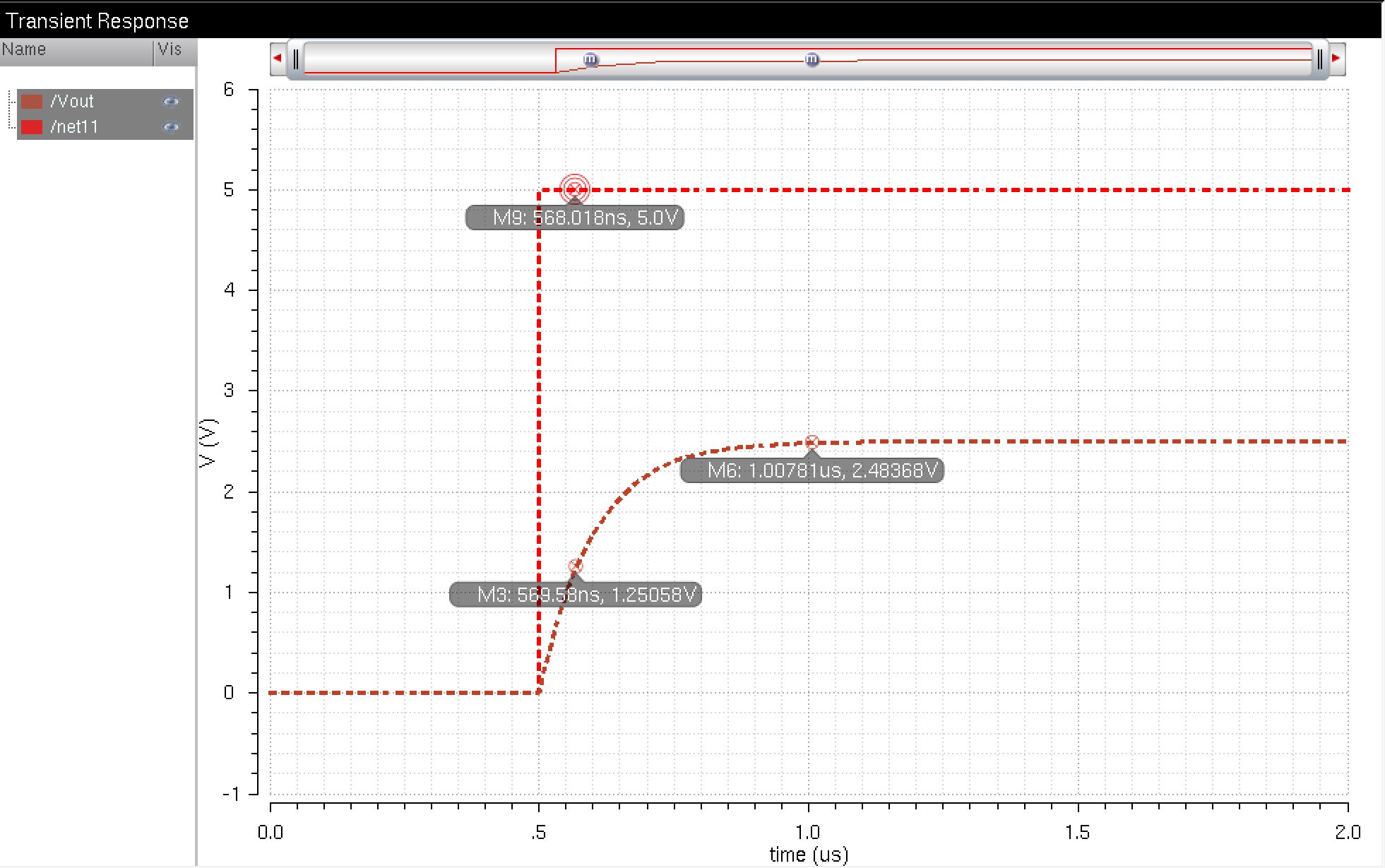
Here we can see that the it takes approximately 69.5 ns to reach half of the maximum value of 2.5V, which proves that the hand calculations were correct.
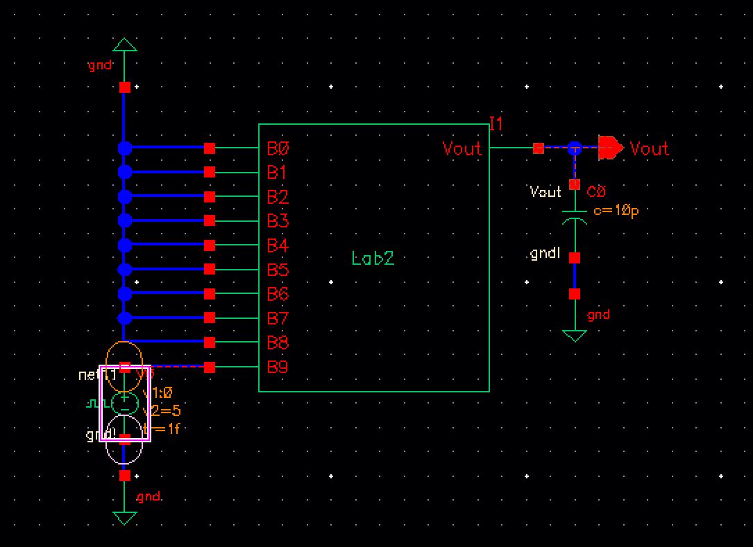
How to create a symbol view:
To create a symbol view, I used the schematic that I created for the 10-bit Ideal DAC. I named the schematic "Lab2". After creating the desired schematic I went to the top of the windows and selected "Create" -> "Cellview" -> "From Cellview ..." then hit OK twice.
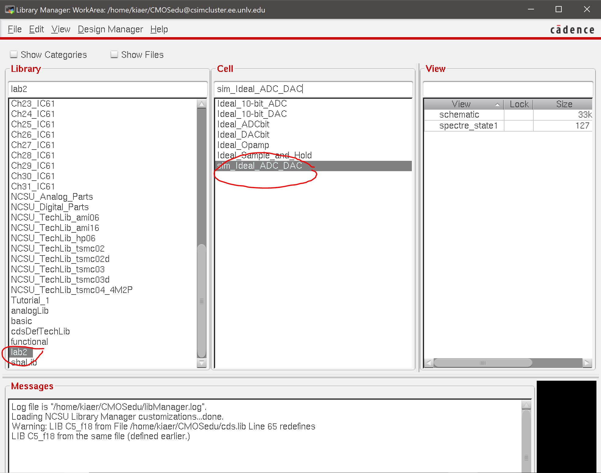
Then a symbol view will appear within the cell in this case "Lab2". To verify that it works I copied the cell and called it "sim_Ideal_DAC" and ran a simulation using the Lab2 symbol.
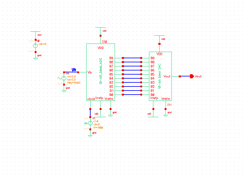
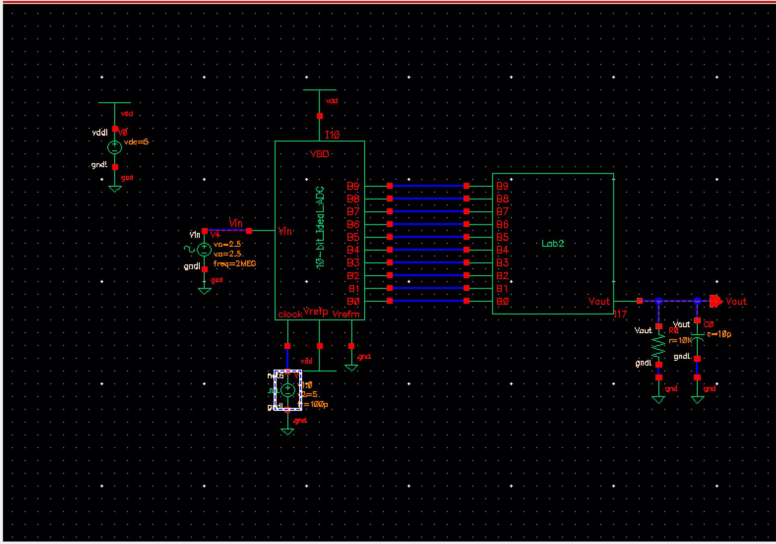
Here is the sim_Ideal_ADC_DAC schematic implemented with my DAC symbol. I had to create a new cell called "sim2_Ideal_ADC_DAC" and then remove the previous DAC in the schematic view and input my own DAC symbol from my Lab2 cell with no load.
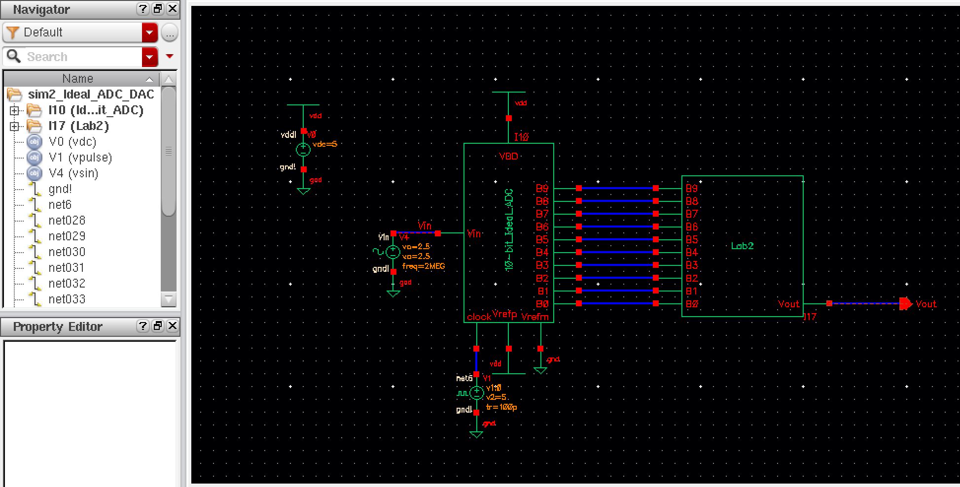
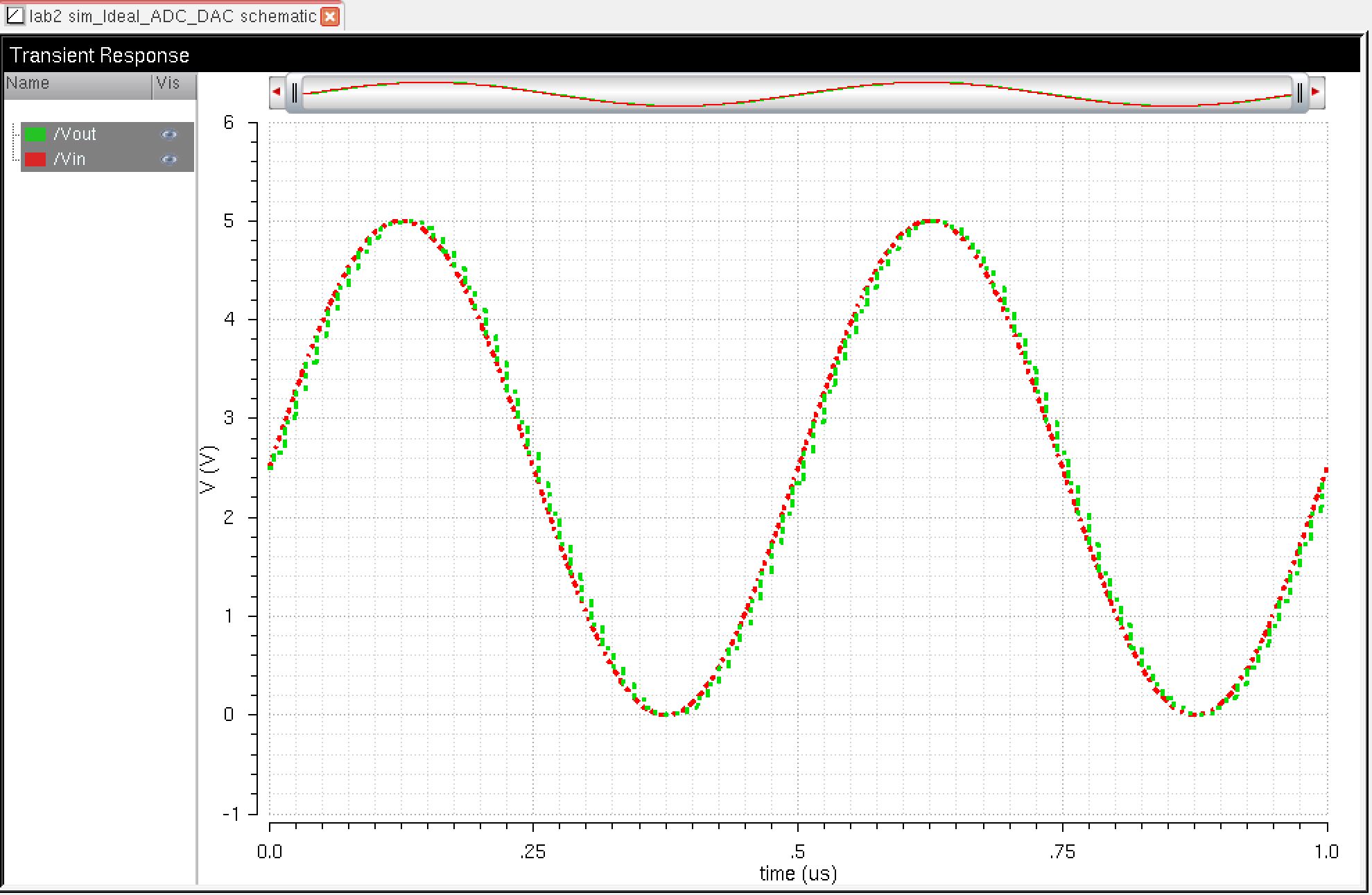
The output is the exact same as the original sim_Ideal_ADC_DAC schematic shown below in detail.
Here is the same schematic but witha 10K resistive load:
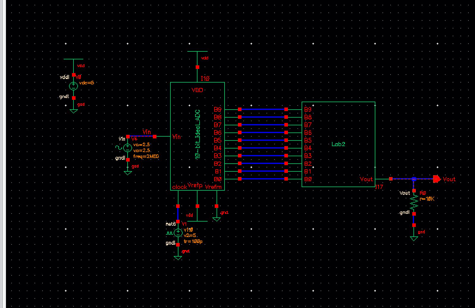
The Transient Response shows that when a 10k resistive load is used the schematic acts like a voltage divide where the output is half of the input. We can also see that they have similar phases as well.
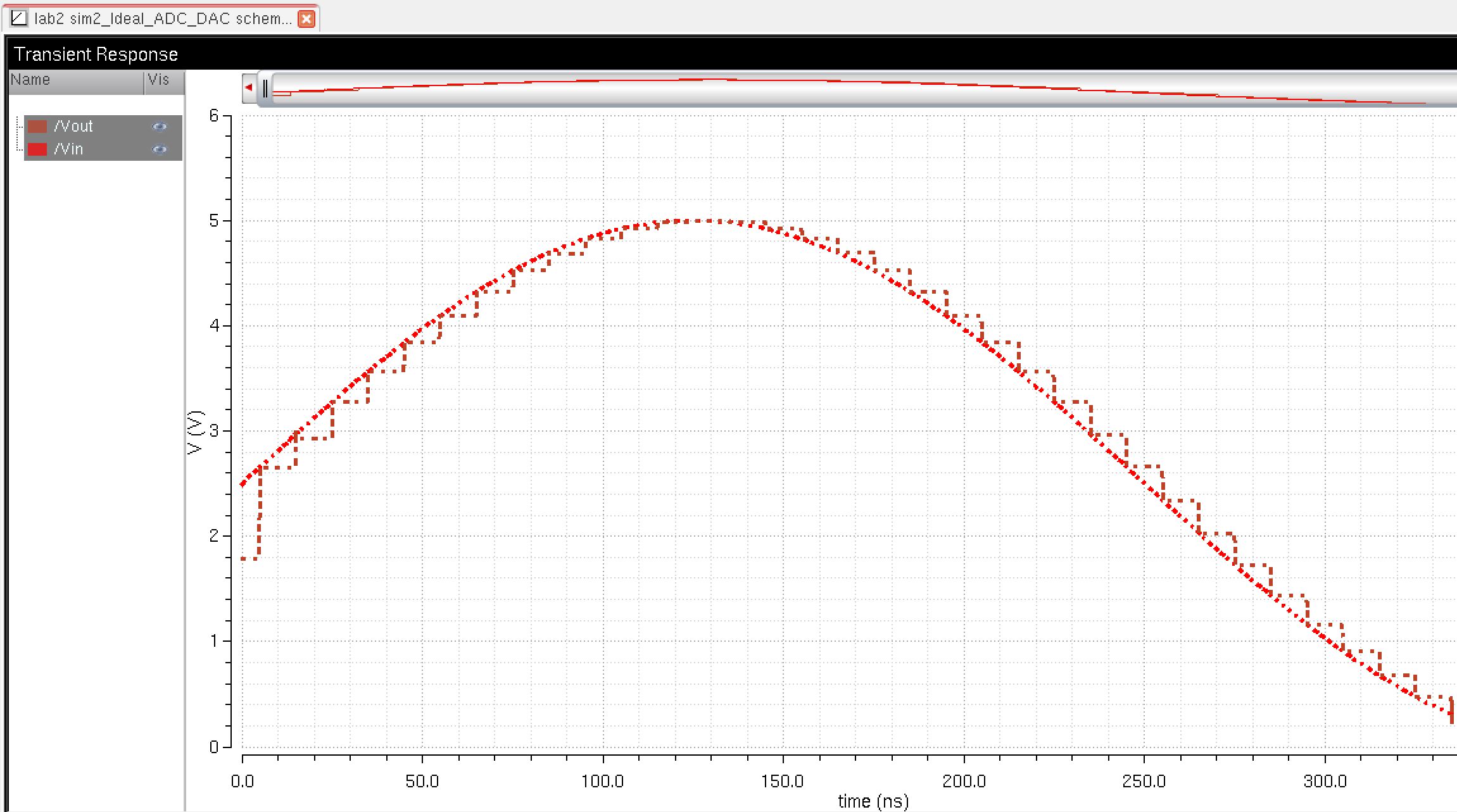
Here is the same schematic but with a capacitive load of 10pF instead of the 10k resistive load.
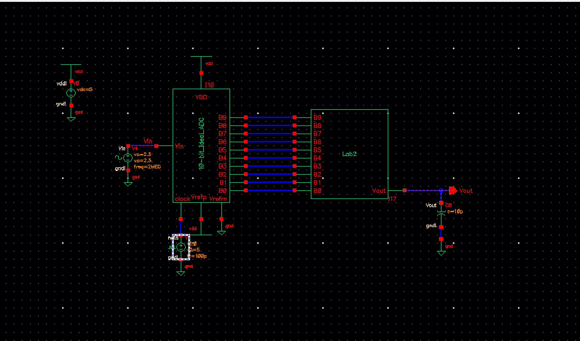
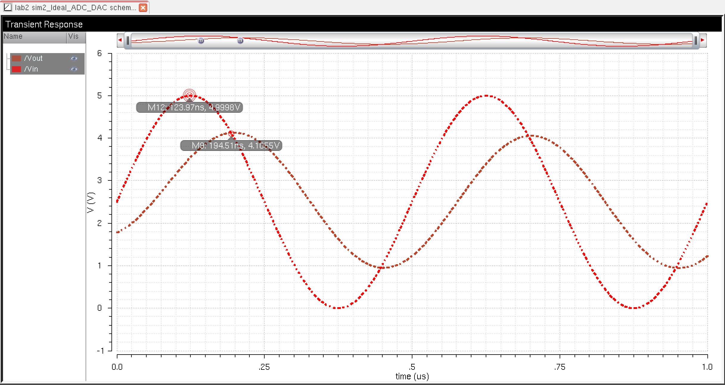
Below is the transient response for 1us using the capacitive load of 10pF. We can see that there is a delay of approximately 70 ns which is accurate with the RC delay that was calculated earlier.
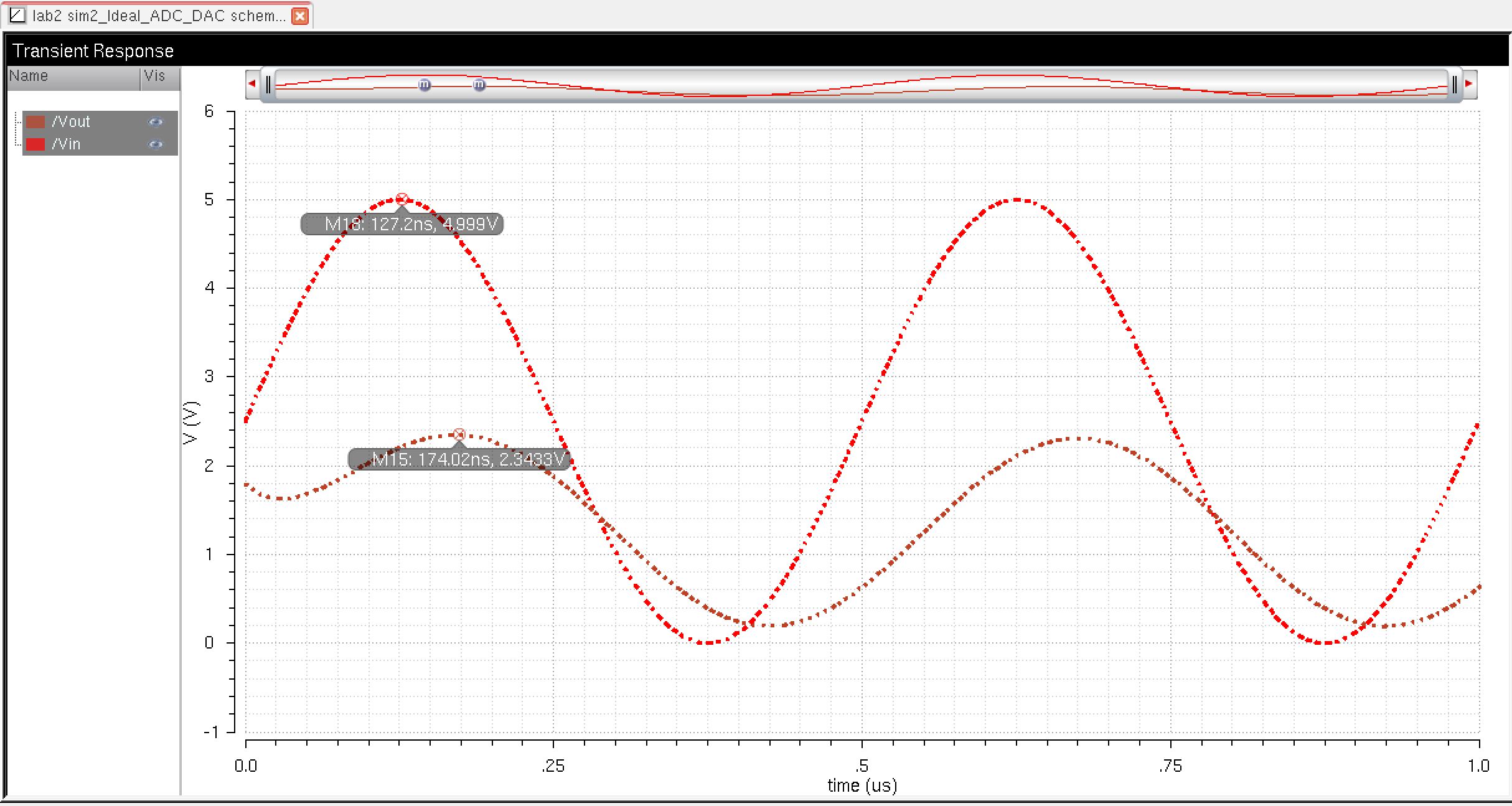
Lastly, here is the schematic with both an RC load with a resistor of 10k and a capacitance at 10pF. We can see that the difference between Vin and Vout is much larger and the delay between the two peaks are about 47ns.
The transient response for the schematic above at 1 us, the delay between Vin and Vout is approximately 47ns.
Discuss what happens if the resistance of the switches isn't small compared to R.
If the resistance of the switch isn't small compared to R then the output resistance would not be R anymore. Furthermore, the higher the resistance the output voltage will dissipate causing less of a difference between Vin and Vout.

To ensure that I have a backup of all the files within Cadence and this lab project, I created a compressed file (.zip) saved on my Desktop and emailed it to myself with a subject title "Lab2_Backup" to make sure I can retrieve the backup files just in case.