Project - EE 421L
Guidelines:
Project (not a group effort, each student will turn in their own project) – design a serial-to-parallel converter that takes
serial input data and an associated clock signal and generates an 8-bit output (parallel) word and clock.
The inputs to your circuit are Din and clock_in.
The outputs to your circuit are D0-D7 and clock_out.
If the serial input is 10 Mbits/s then the parallel output is 1.25 MWords/s.
First half of the project (just the serial-parallel converter schematics, no layout), of your design and an html report detailing
operation (including simulations), is due at the beginning of lab on Nov. 14.
Your serial-parallel design should show various inputs to verify it works
Put your report (proj.htm) in a folder called /proj in your directory at CMOSedu and link to your index.htm page.
Dr. Baker will go over your design with you, including running simulations, when lab meets on Nov. 14.
Second half of the project, a verified layout and documention (in html), is due at the beginning of lab on Nov. 21.
Dr. Baker will meet with you on Nov. 21 to go over your layout and, again, put your report in the /proj folder in your directory at CMOSedu.
Ensure that there is a link on your project report webpage to your zipped design directory.
The following image sizes can be increased by simply clicking on the images.
----------------------------------------------------------------------------------------------------
Part 1: Prior to constructing the 8-bit Serial-to-Parallel Converter, we need to construct one of the main components, the D-Flipflop.
The D-flipflop will be extensively used within this project which we will have to construct first.
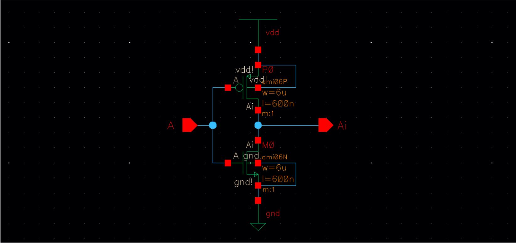
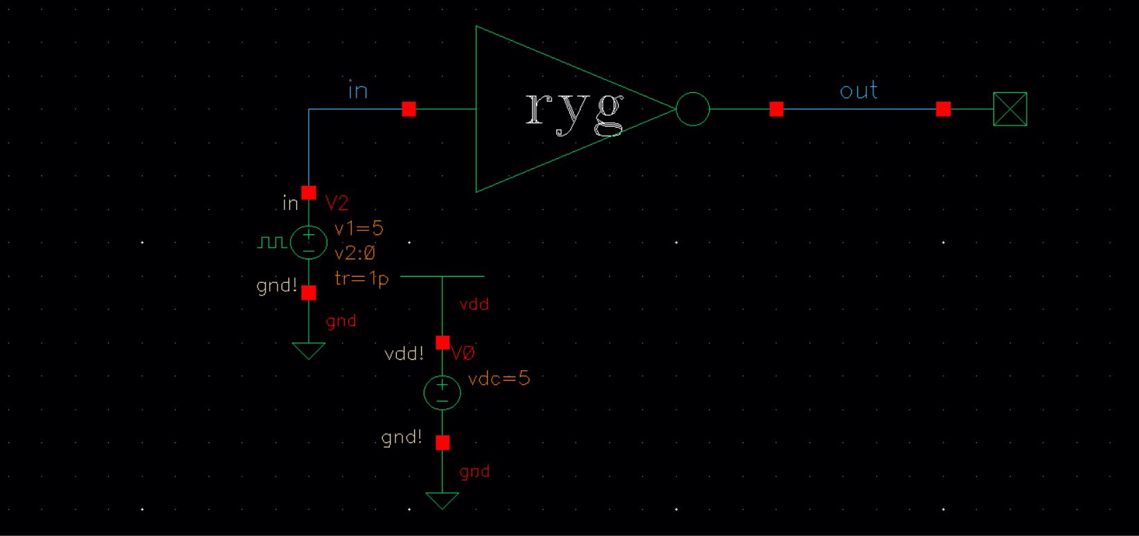
Step 1: The D-Flipflop will be comprised of Transmission Gates and Inverters. Design and Simulate the Transmission Gate and Inverter.
The following provides the schematics and symbols used for the Transmission Gate and Invereter.
| Transmission Gate Symbol | Transmission Gate Schematic |
| |
| Inverter Symbol | Inverter Schematic |
| |
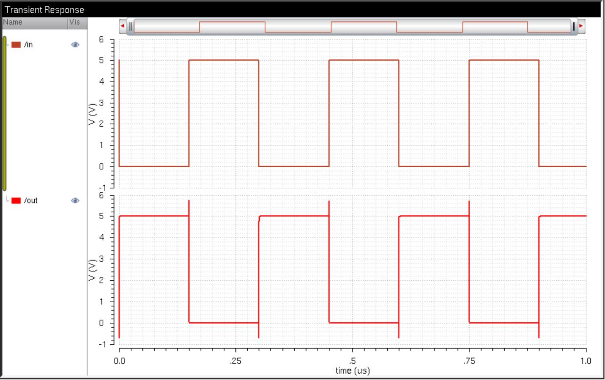
The following images are simulations to the transmission gate and inverter.
| Transmission Gate Simulation Schematic | Transmission Simulation Output |
 |  |
| Inverter Simulation Schematic | Inverter Simulation Output |
 |  |
Step 3: Design and Simulate the operation for a 1/8th reduced clock schematic using D-Flipflop.
Step 2: Design and simulate the operation for a Edge-Trigger D-Flipflop,
As previously mentioned, transmission gates and inverters will be used to create the D-Flipflop.
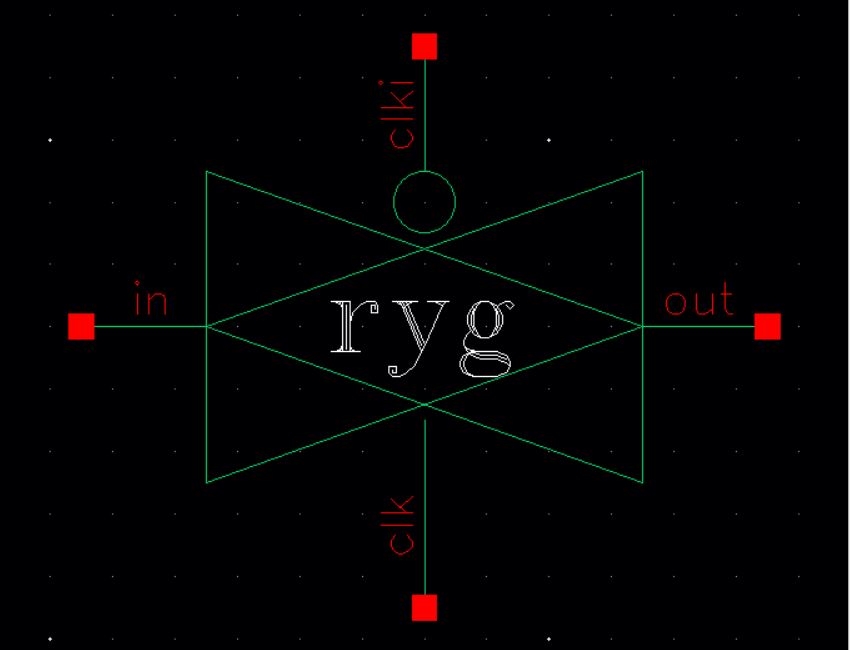
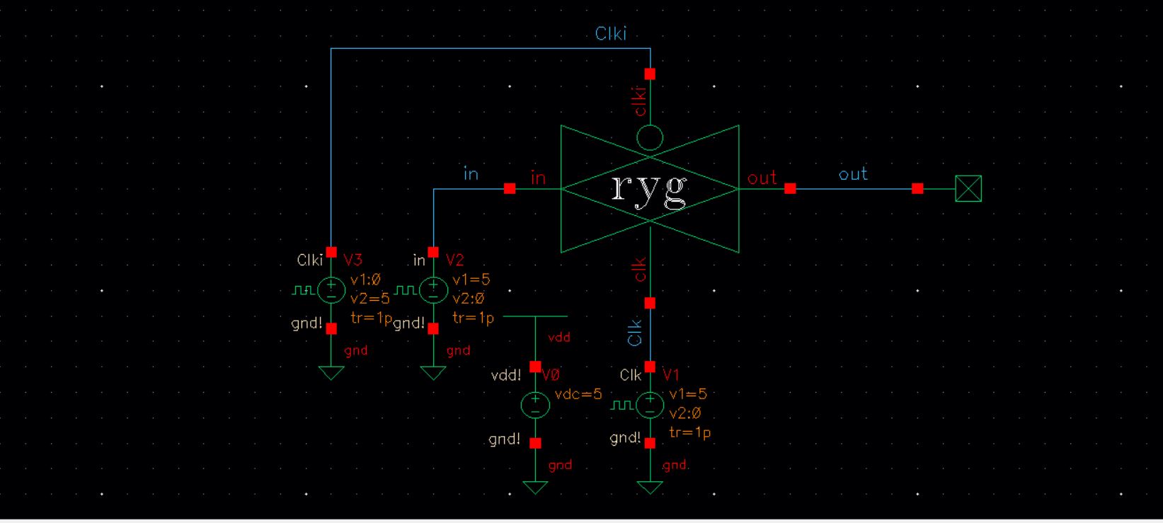
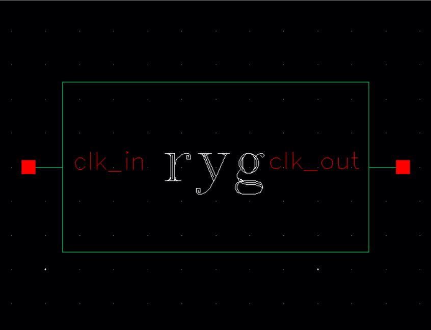
| D-Flipflop Symbol | D-Flipflop Schematic |
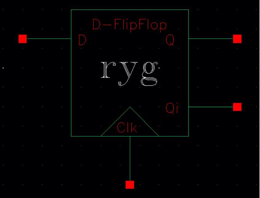 |  |
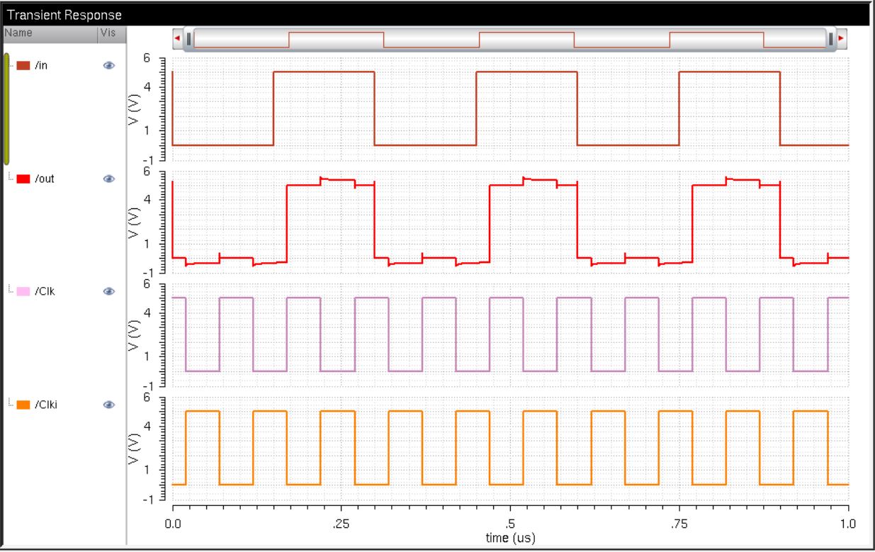
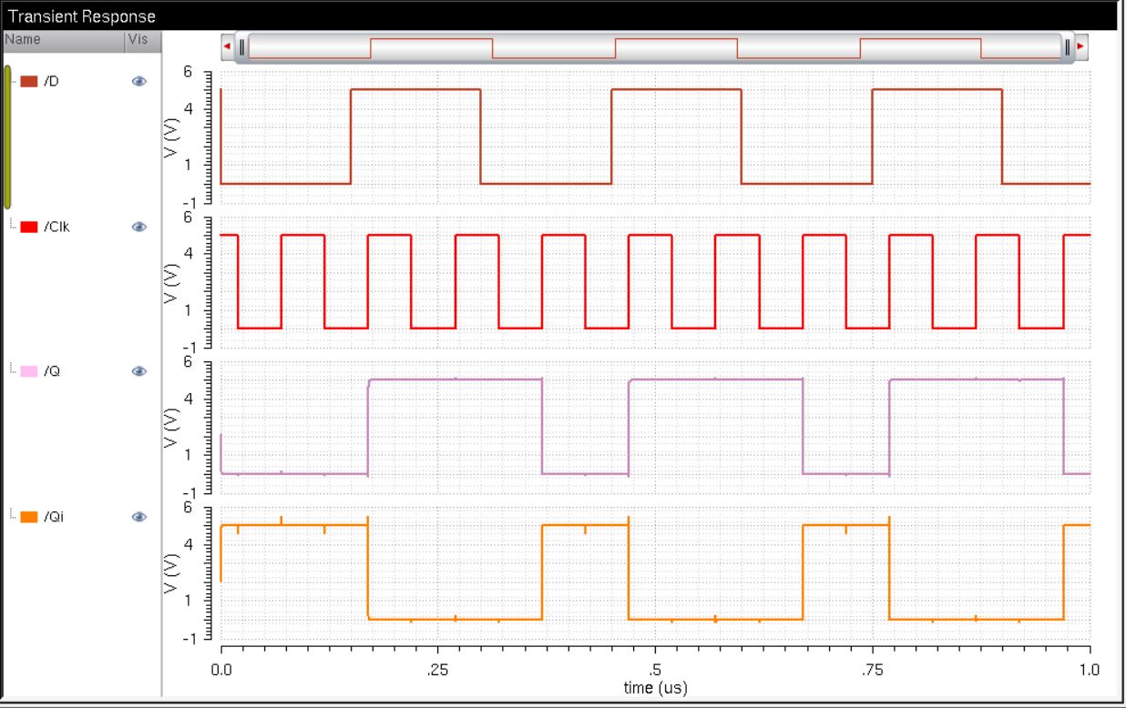
When simulating the D-Flipflop operation, we can check that it is indeed edge-triggered.
When 'Q' changes from high-to-low or low-to-high, we can observe that the clock changes on thefalling of the clock.
Therefore, 'Q' is the value of 'D' every falling edge of the clock.
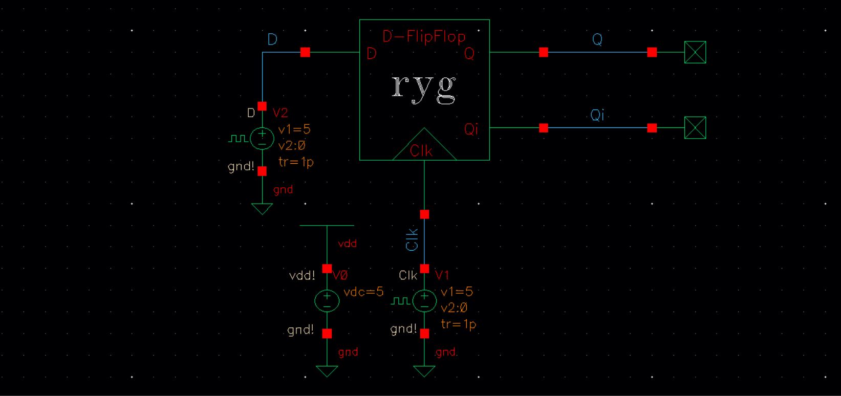
| D-Flipflop Simulation Schematic | D-Flipflop Simulation Output |
 |  |
Step 3: Design and Simulate the operation for a 1/8th reduced clock schematic using D-Flipflop.
By feeding the inverted Q-output into the D-input, the regular Q-output will have a reduced clock cycle by a half (or x2 slower).
In order to reduce the clock cycle by 1/8th, we will need to attach the configuration in series.
The Q-output will feed into the clock-input of another D-Flipflop twice.
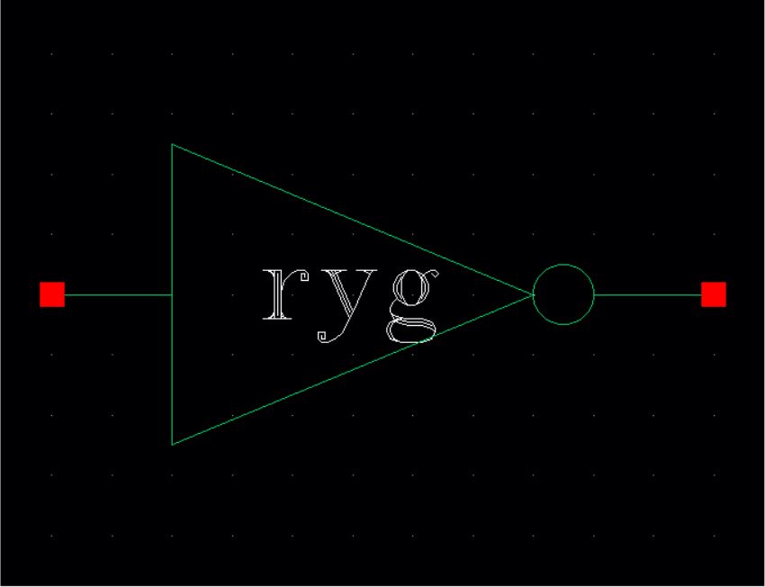
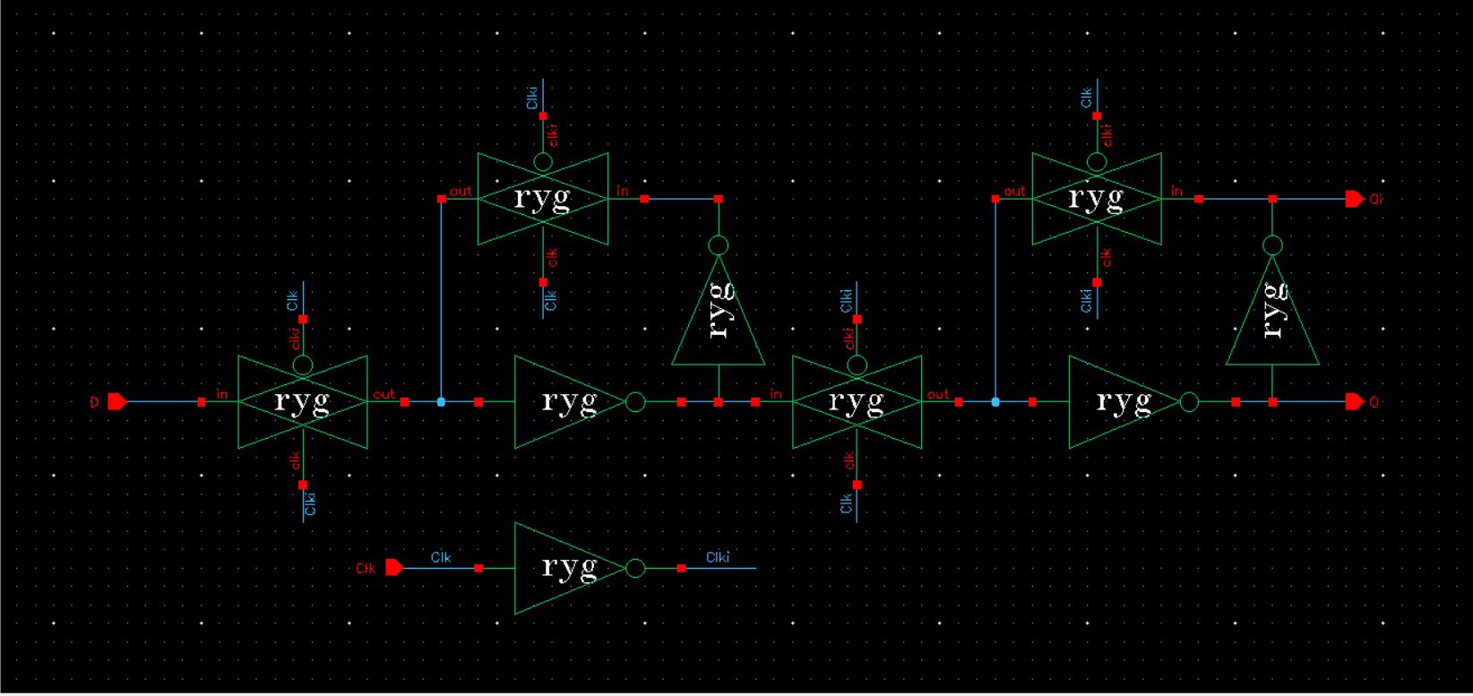
| 1/8th Reduced Clock Symbol | 1/8th Reduced Clock Schematic |
 | 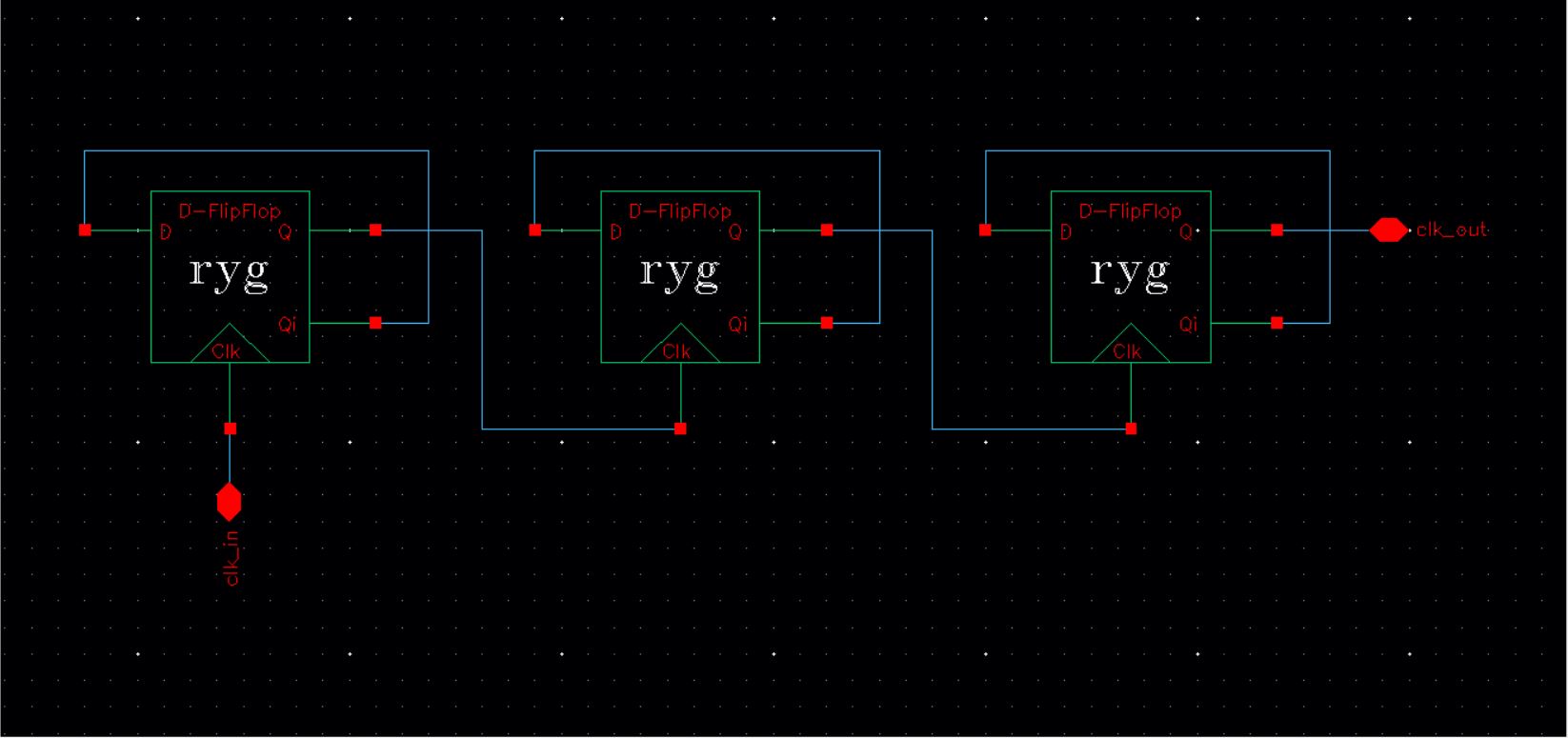 |
We can see that from the first D-Flipflop configuration, we've reduced the clock cycle by half.
By connecting the configuration into another D-Flipflop, we further reduce the clock by half.
Thus, with 3 D-Flipflops in series with the same configuration, we can reduce the clock by 1/8th in the final output.
| 1/8th Reduced Clock Simulation Schematic | 1/8th Reduced Clock Symbol Simulation Output |
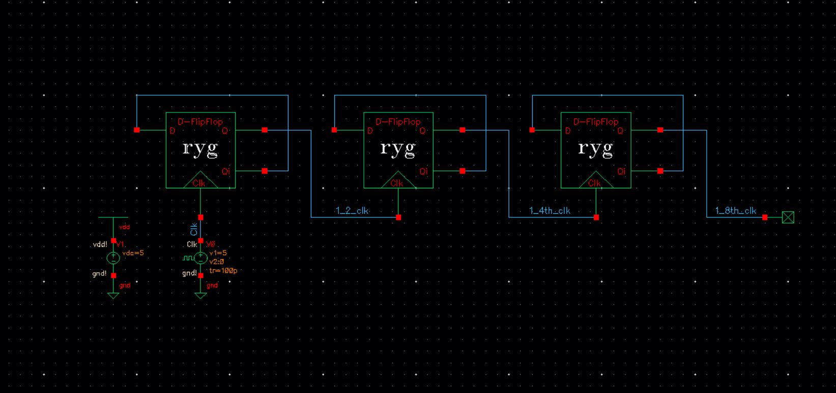 | 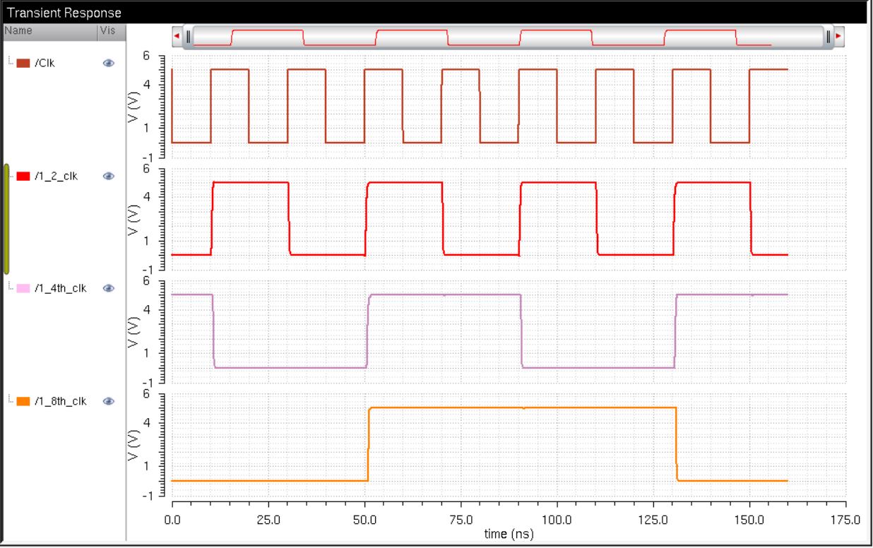 |
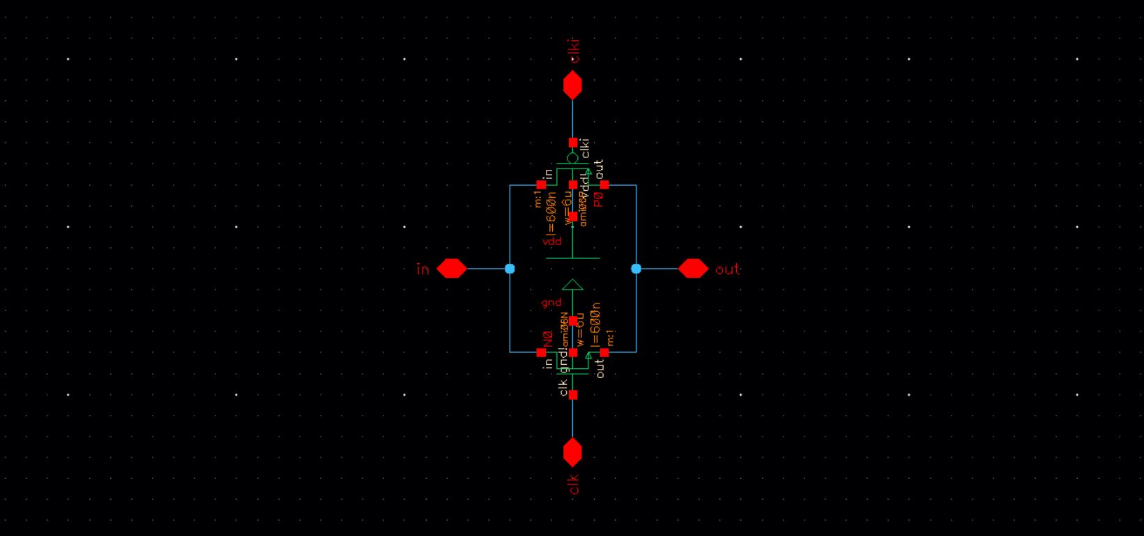
Step 4: Design and Simulate the operation for a Serial-to-Parallel converter.
In order to create a Serial-to-Parallel converter, we need 2 rows of registers.
-> The first row of registers (bottom on the schematic) will feed the serial input data through 'Din' with a fast clock signal (10 Mbits/s).
-> The second row of registers (top on the schematic) will receive each of the bits simultaneously, but only output every 8th cycle (1.25MWords/s).
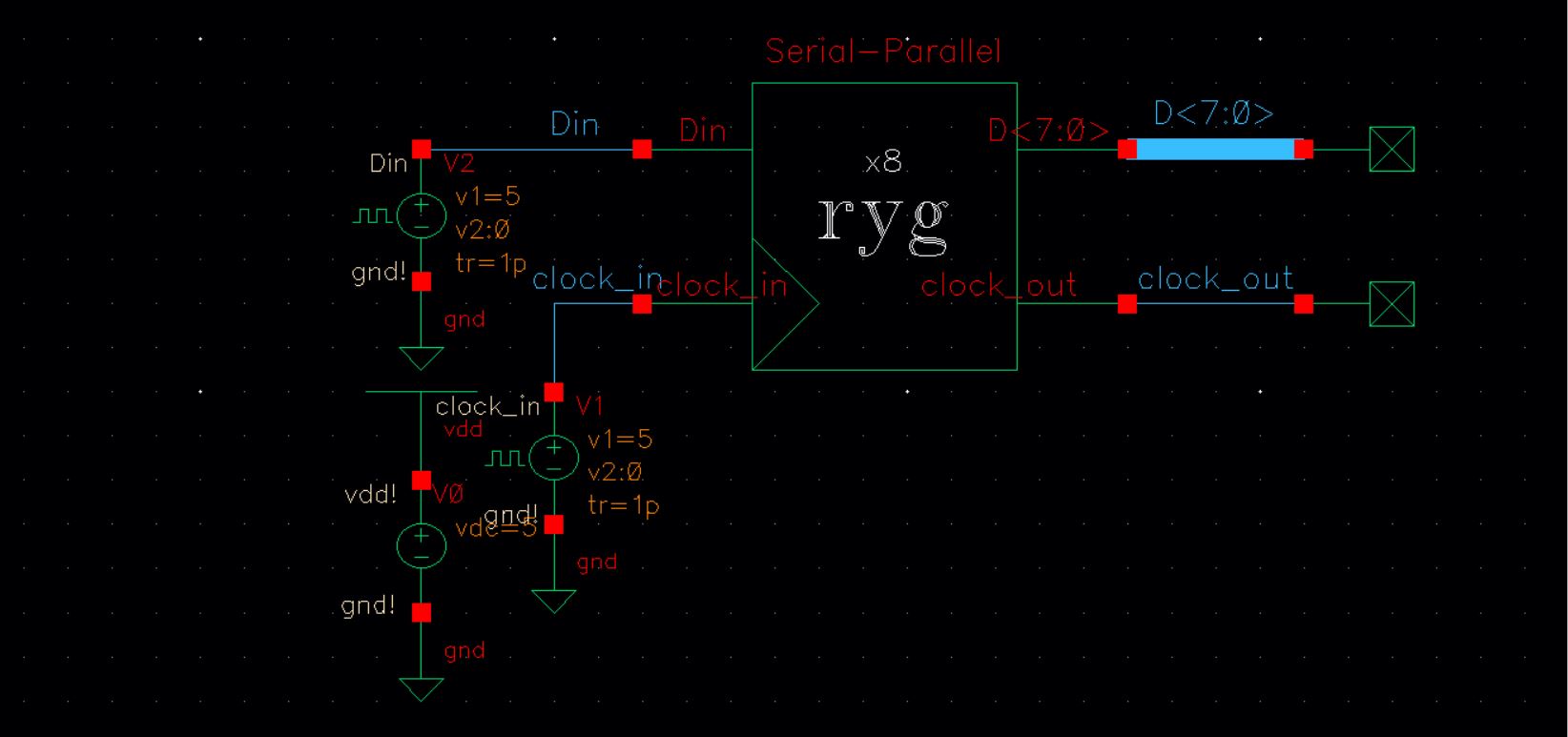
| Serial-to-Parallel Converter Symbol | Serial-to-Parallel ConverterSchematic |
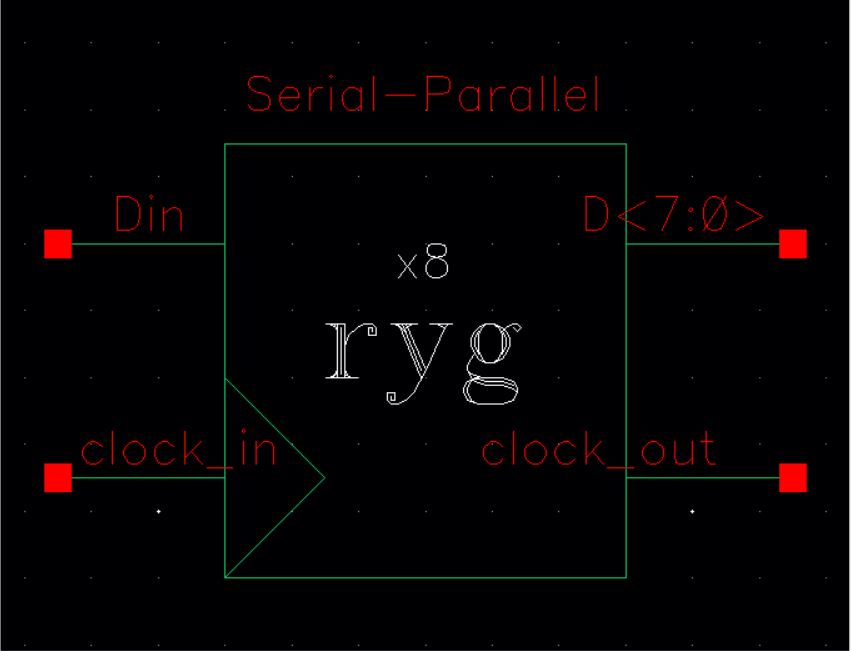 | 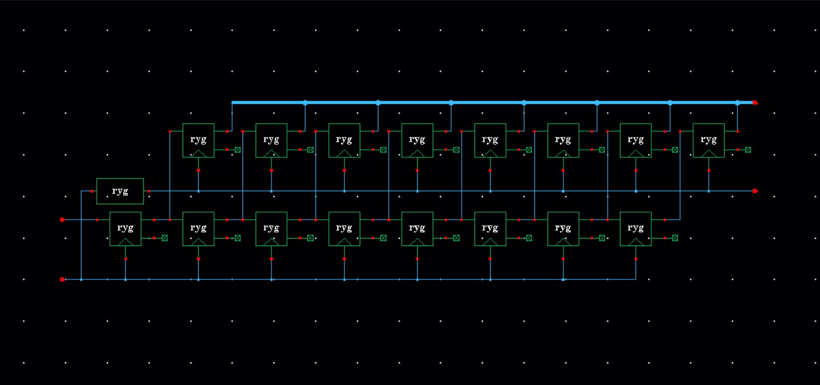 |
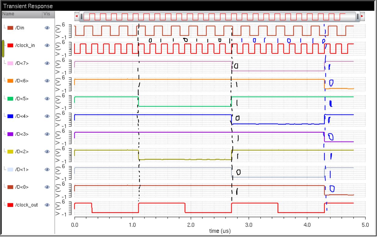
We can see that a single input is feeding a line of low and high voltages (bits) through 'Din',
On the rising edge of clock, the values are taken from 'Din'.
The bits 'D7-D0' represent the Word (8-bits) from 'Din'.
There is some delay since clock does begin a little later causing the reduced clock and output bits to show later.
| D-Flipflop Simulation Schematic | D-Flipflop Simulation Output |
 |  |
This concludes the operation for a Serial-to-Parallel Converter for Part 1.
----------------------------------------------------------------------------------------------------
Part 2: The following report will discuss the layout procedure for the Serial-to-Parallel converter.
(Due: 11/20/18)
Step 1: Layout and extract the components used to create the serial-to-parallel converter including the final schematic.
| Layout | Extraction | |
| Transmission Gate |  |  |
| Inverter |  |  |
| D-Flipflop | 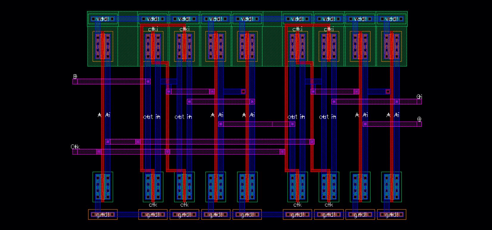 | 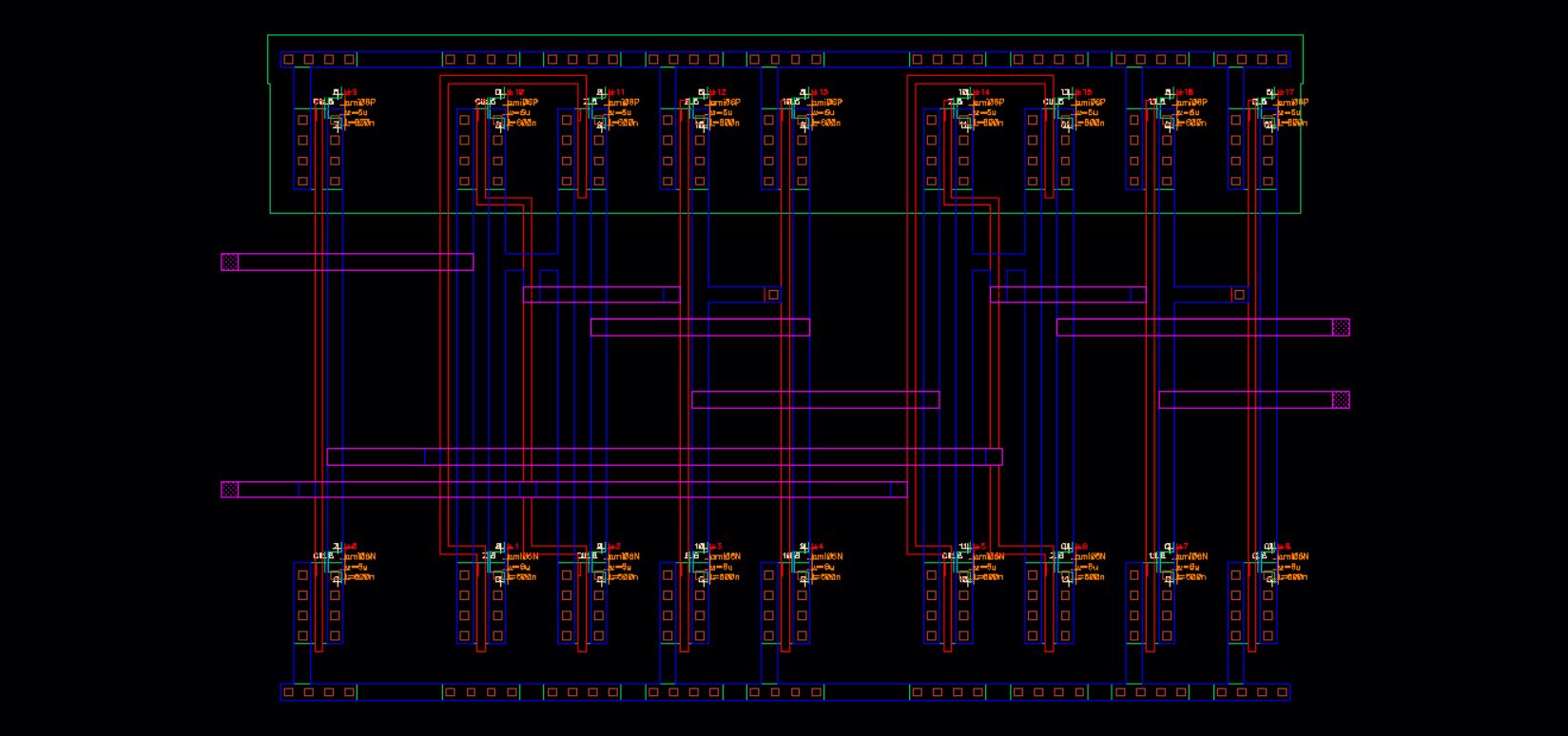 |
| 1/8th Reduced Clock | 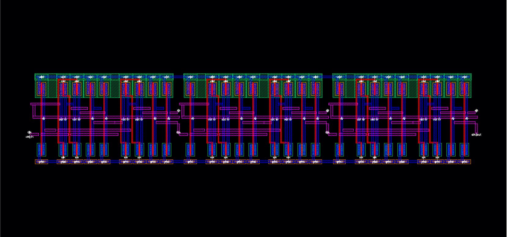 | 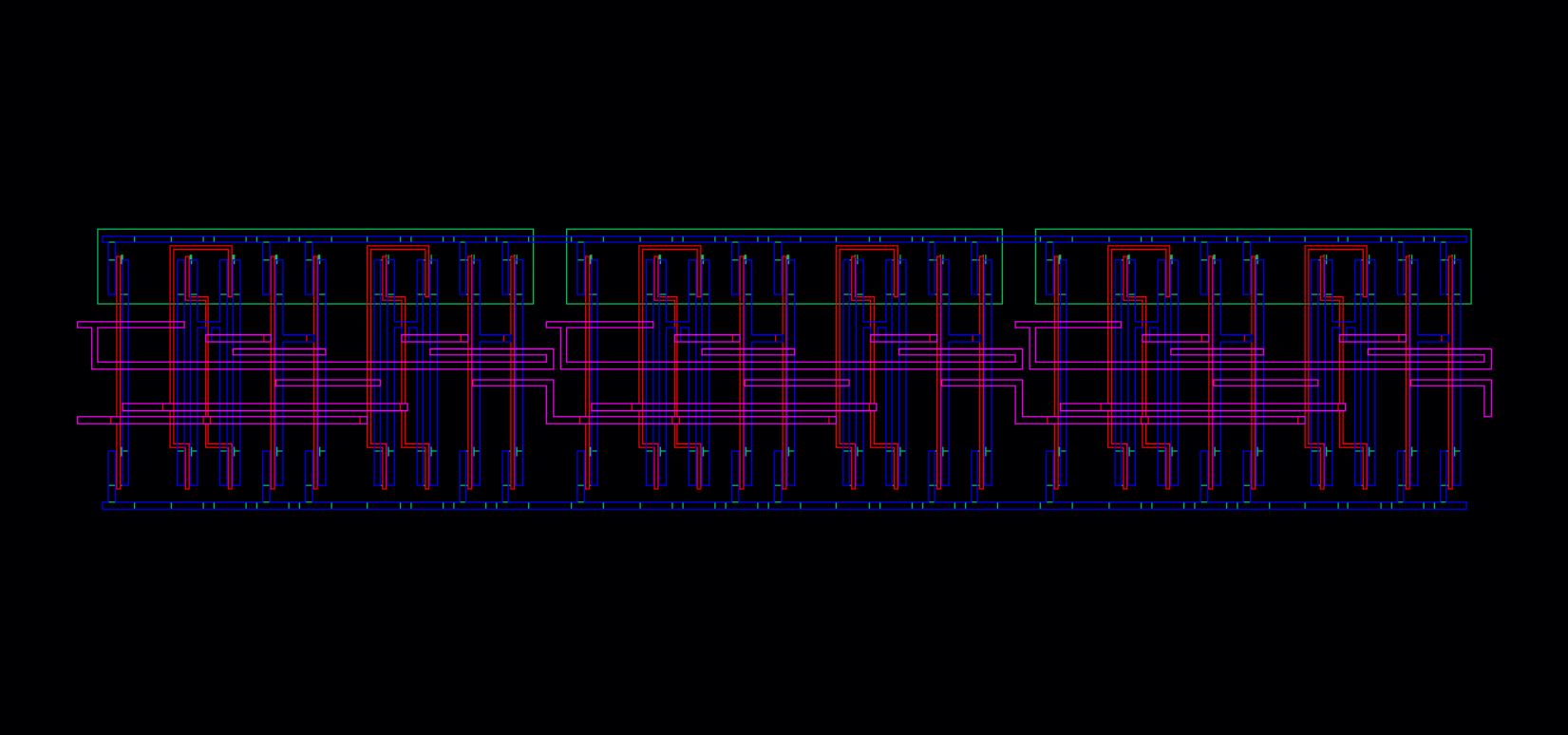 |
| Serial-to-Parallel Converter | 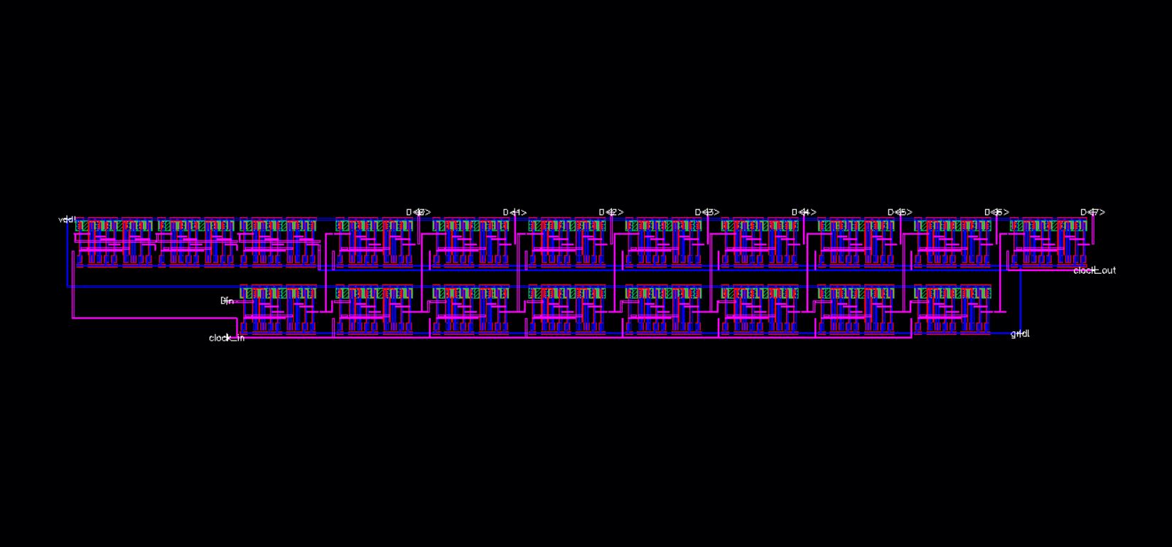 | 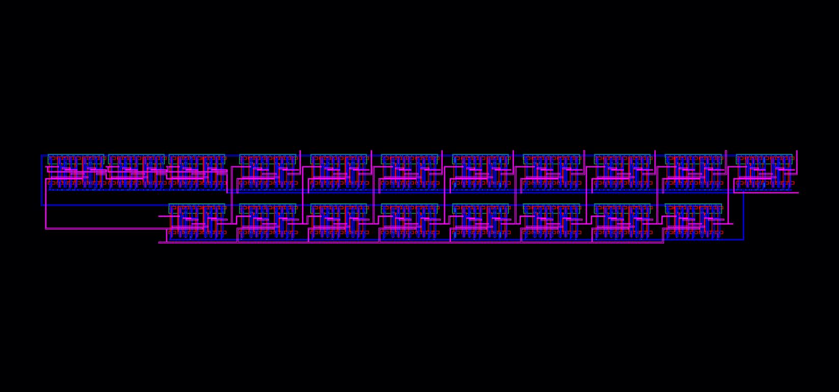 |
Step 2: DRC the layouts.
| Transmission Gate | 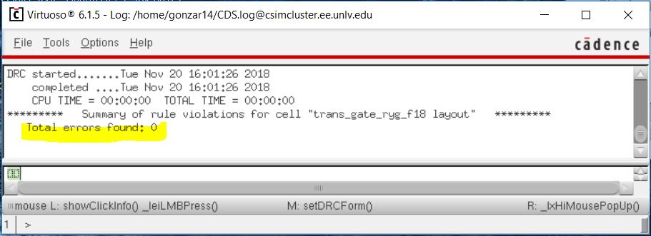 |
| Inverter | 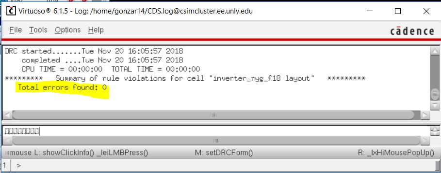 |
| D-Flipflop | 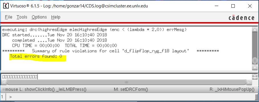 |
| 1/8th Reduced Clock | 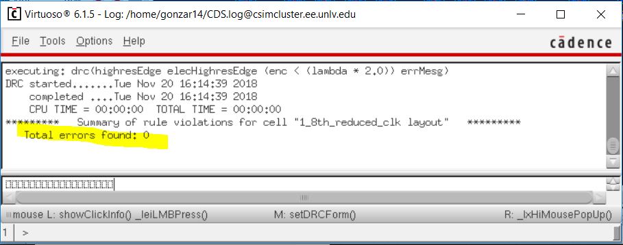 |
| Serial-to-Parallel Converter | 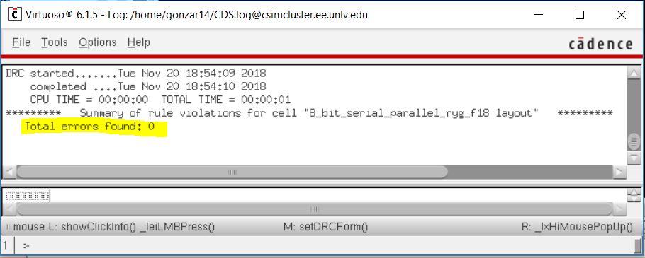 |
Step 3: LVS the extractions to the schematics..
| Transmission Gate | 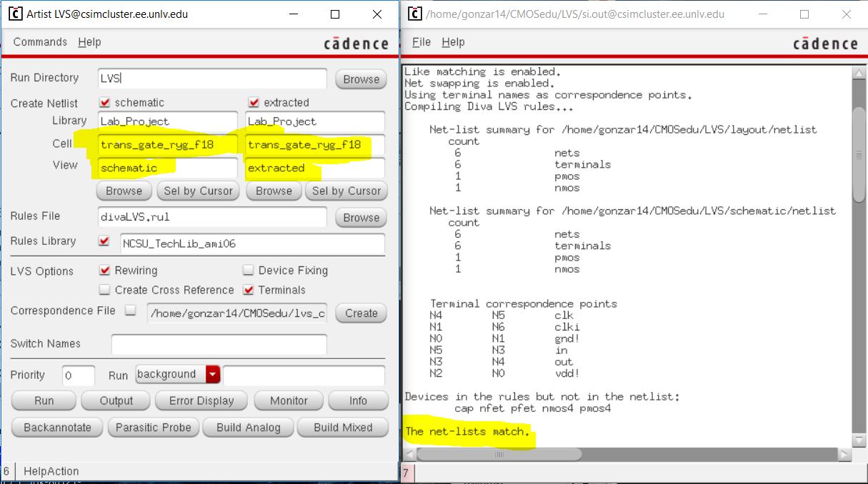 |
| Inverter | 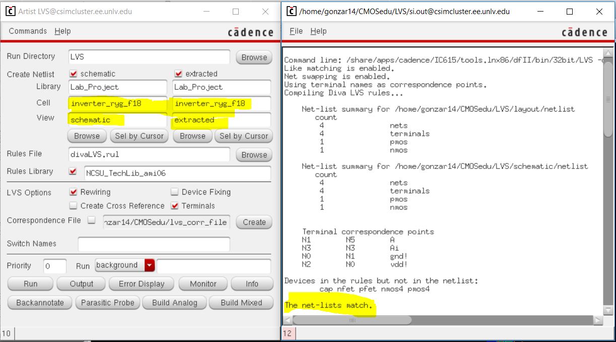 |
| D-Flipflop | 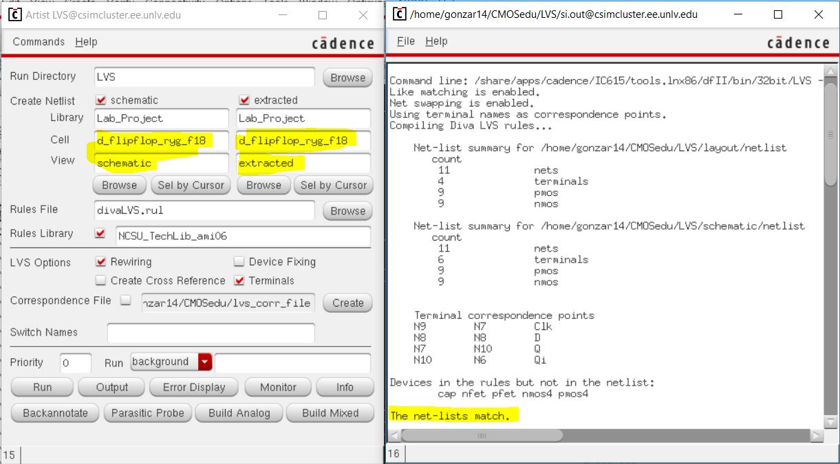 |
| 1/8th Reduced Clock | 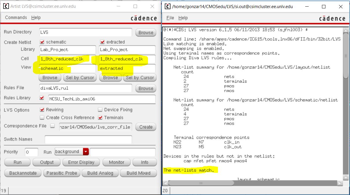 |
| Serial-to-Parallel Converter | 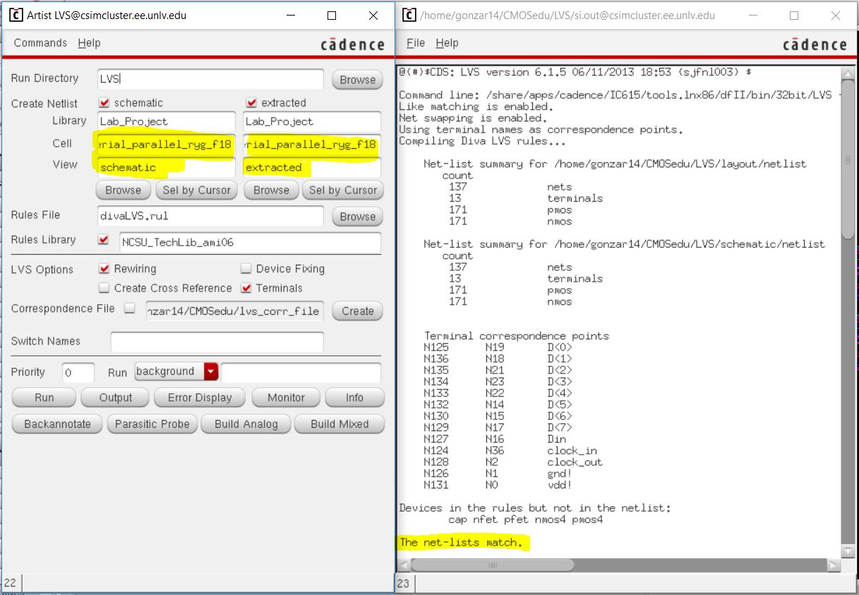 |
The following directory to the project can be downloaded through this link.
----------------------------------------------------------------------------------------------------
The design directory is downloaded from the MobaXterm server and backed up onto this website (Up-to-date 11/20/18).
-> They are stored into my backup folder on my laptop and also on my online drive.
The CMOSedu directory has been backed up, and my following lab design directories will be continued to become backe up.
----------------------------------------------------------------------------------------------------
This Concludes the Project Report.