Lab 06 - EE 421L
----------------------------------------------------------------------------------------------------
Prelab:
The labs are backed up through a saved directory in my computer as well as into my google drive account (Up-to-Date from end of previous lab).
The prelab also demonstrates Tutorial 4 on the CMOSedu website. The image size can be increased by clicking on the images for more detail.
Tutorial 4 was read previously to provide insight for the design process for a logic gate.
This labs will then use the same techniques to recreate NAND, XOR, and a Full-adder.
----------------------------------------------------------------------------------------------------
Lab:
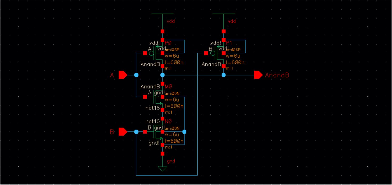
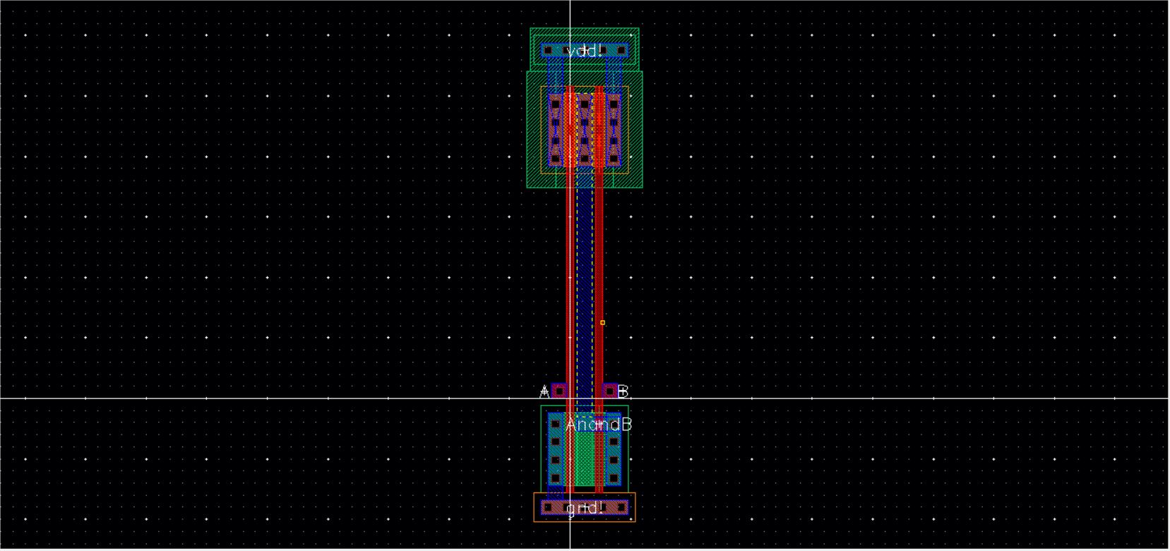
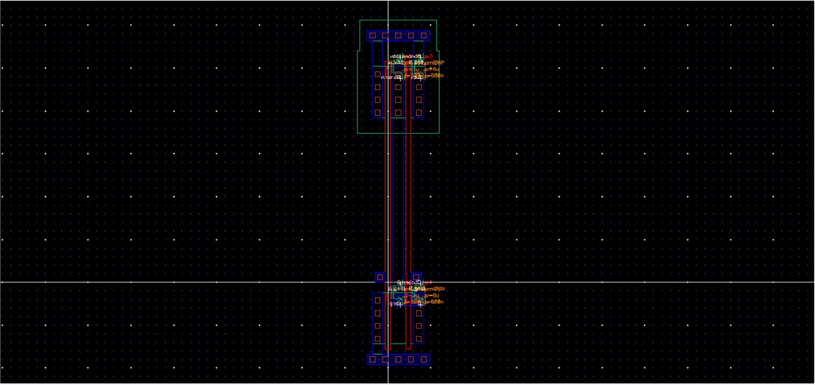
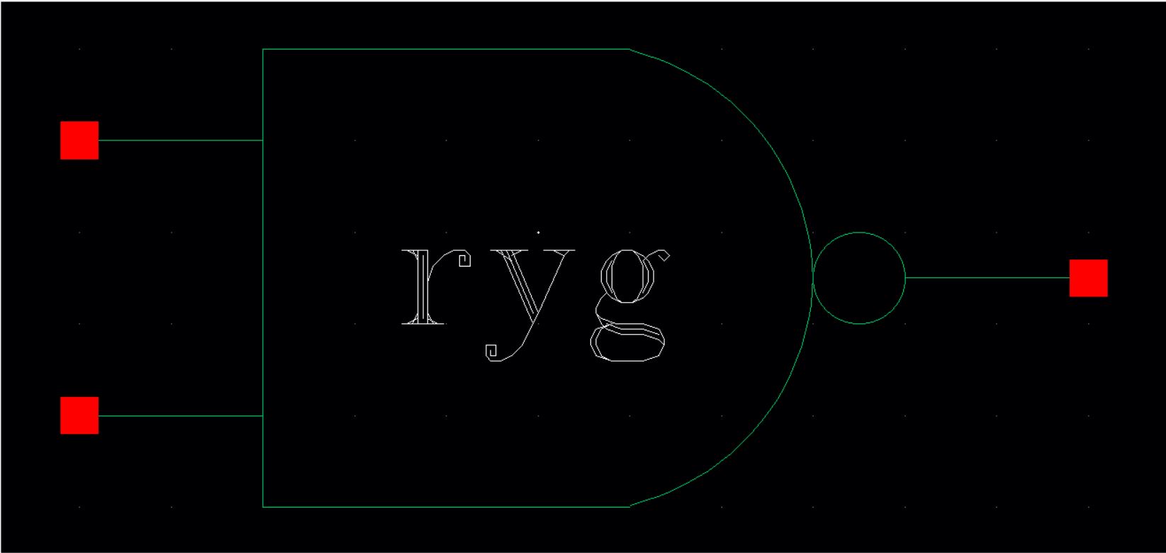
Step 1: Draft the schematics of a 2-input NAND gate (Fig. 12.1), and a 2-input XOR gate (Fig. 12.18) using 6u/0.6u MOSFETs (both NMOS and PMOS).
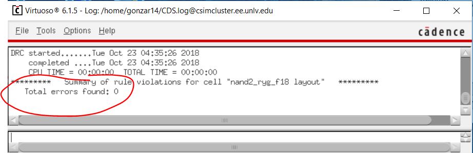
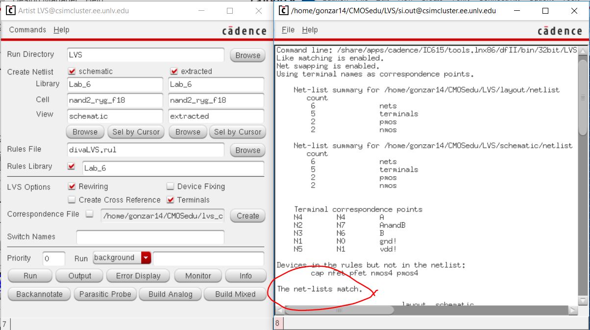
Create layout and symbol views for these gates showing that the cells DRC and LVS without errors.
| NAND Schematic | NAND Layout |
| |
| NAND Extracted | NAND Symbol |
| |
The following images indicate that the DRC/LVS of the Layout for the NAND logic gate had no errors.
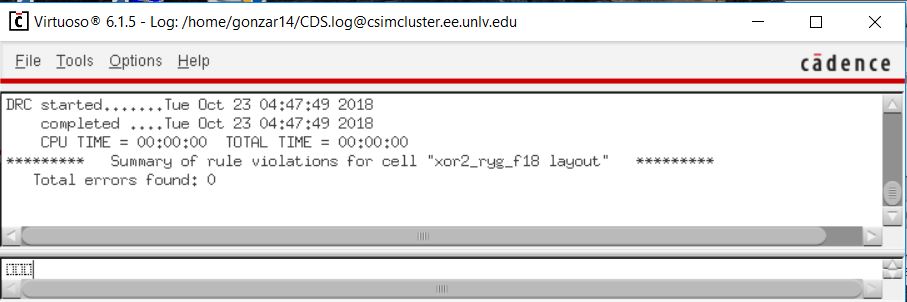
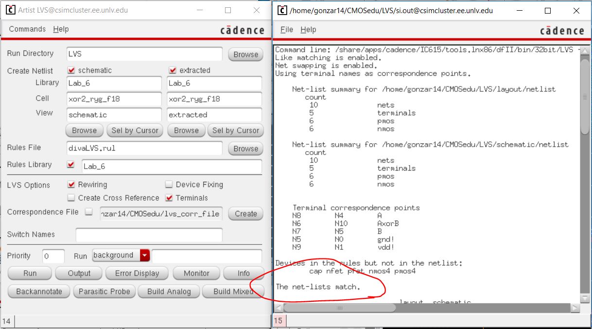
| XOR Schematic | XOR Layout |
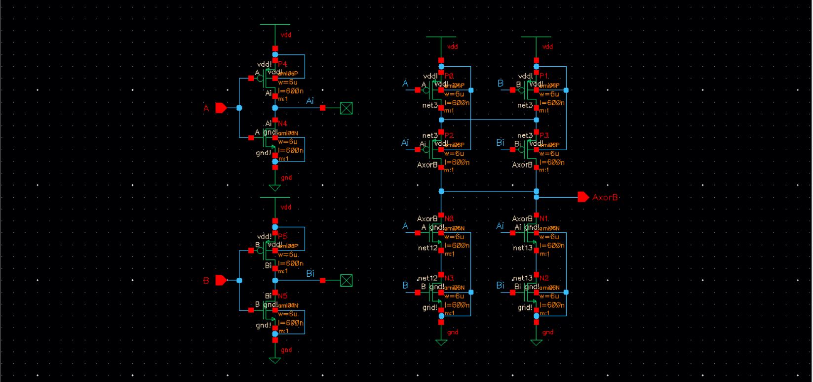 | 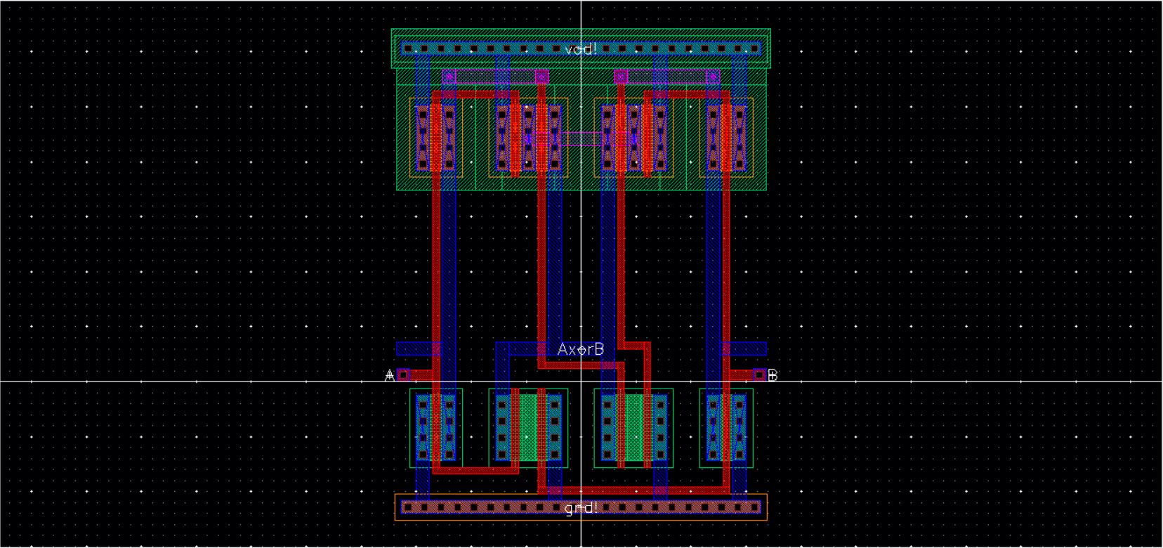 |
| XOR Extracted | XOR Symbol |
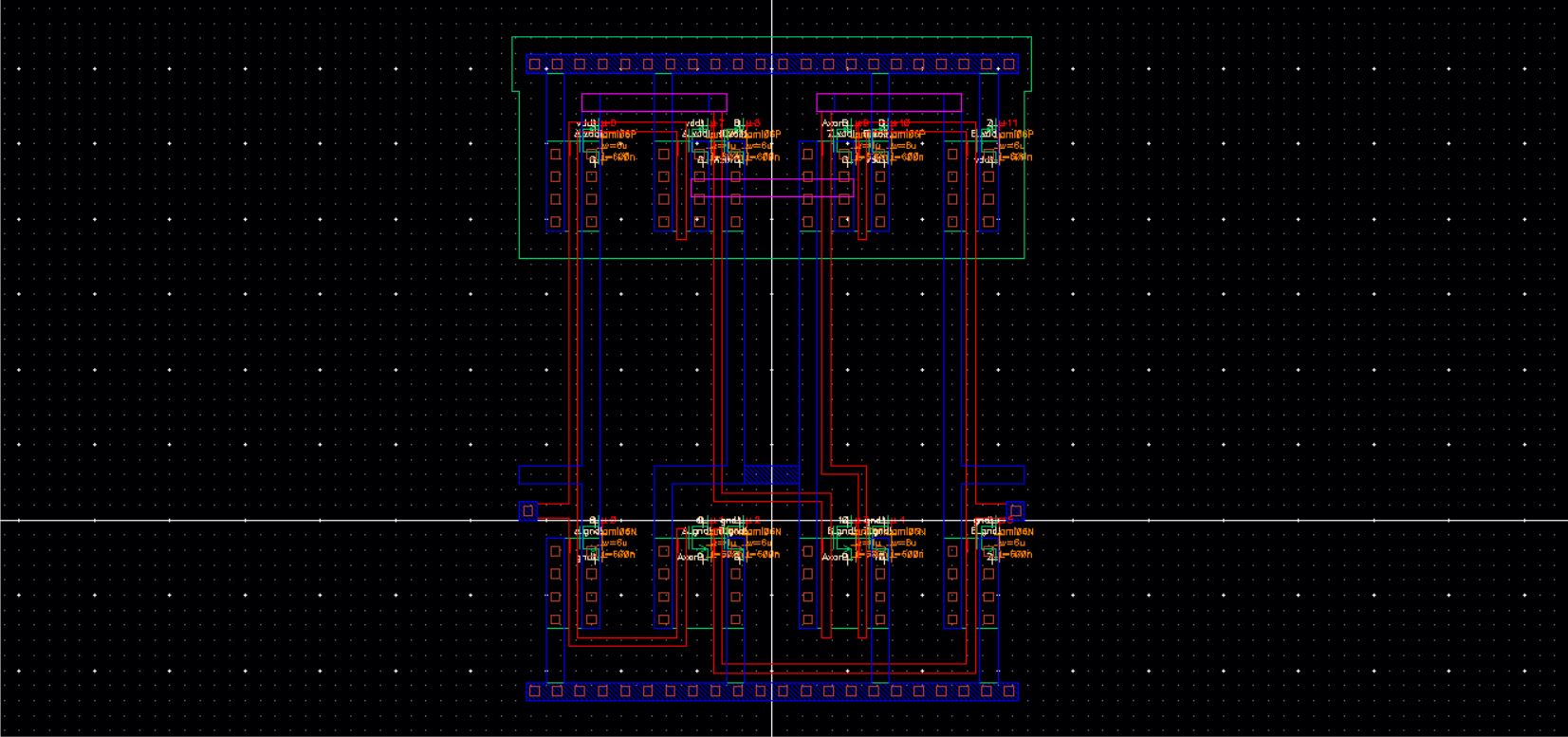 | 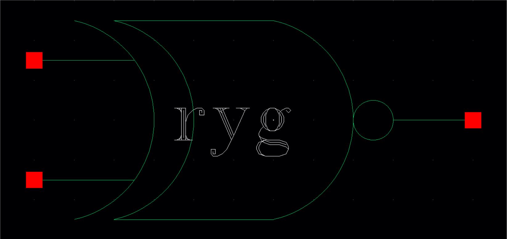 |
The following images indicate that the DRC/LVS of the Layout for the XOR logic gate had no errors.
***These files can be downloaded as a zipped file at the bottom of the end of this lab report.
Step 2: Using Spectre simulate the logical operation of the gates for all 4 possible inputs (00, 01, 10, and 11).
| Gate Simulation Schematic | Gate Outputs |
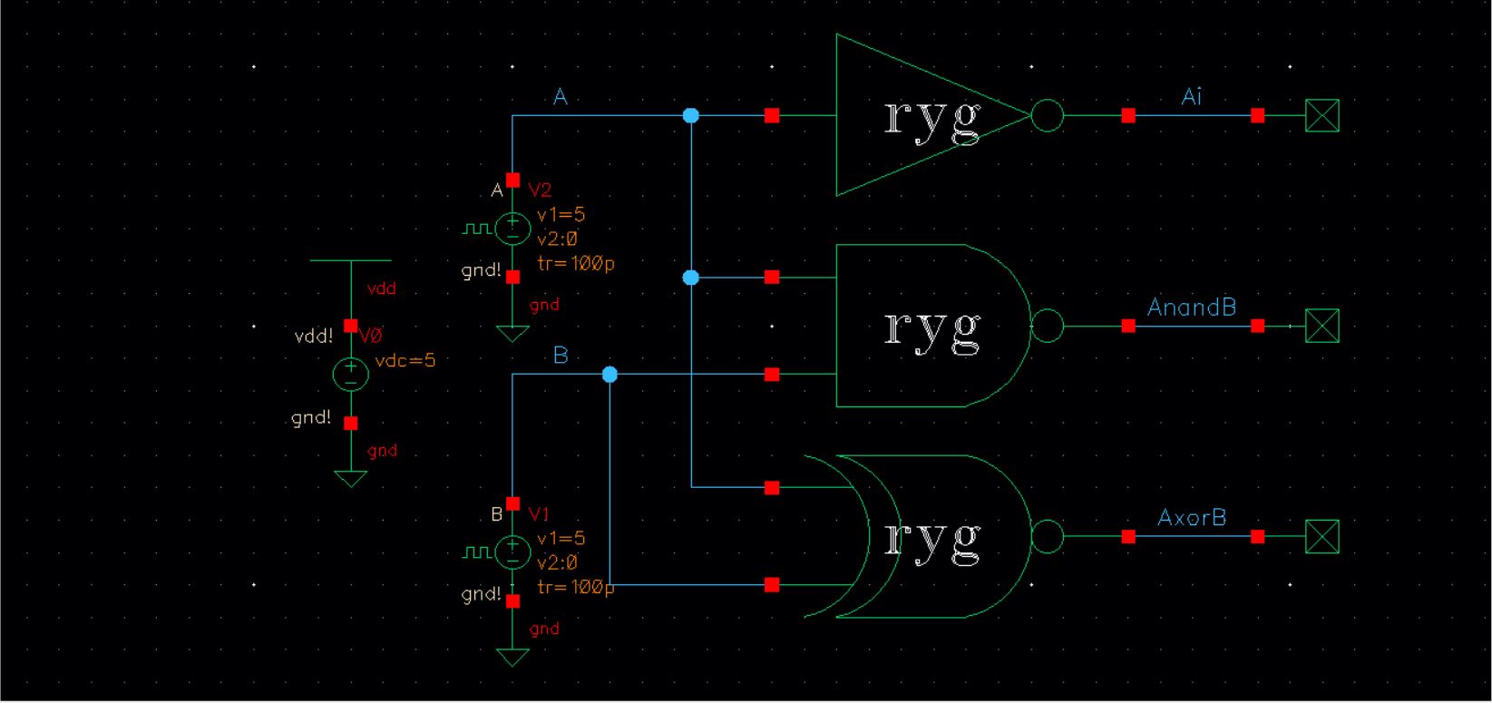 |  |
We can observe that the Inverter, NAND, and XOR logic gates operate correctly. Aso, the changes in the logical ouputs are not perfect.
| A | B | Ai | NAND | XOR | |
| 0 | 0 | 1 | 1 | 0 | |
| 1 | 0 | 0 | 1 | 1 | |
| 0 | 1 | 1 | 1 | 1 | |
| 1 | 1 | 0 | 0 | 0 |
Step 3: Using these gates, draft the schematic of the full adder. Create a symbol for this full-adder.
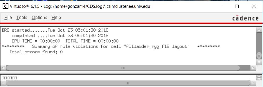
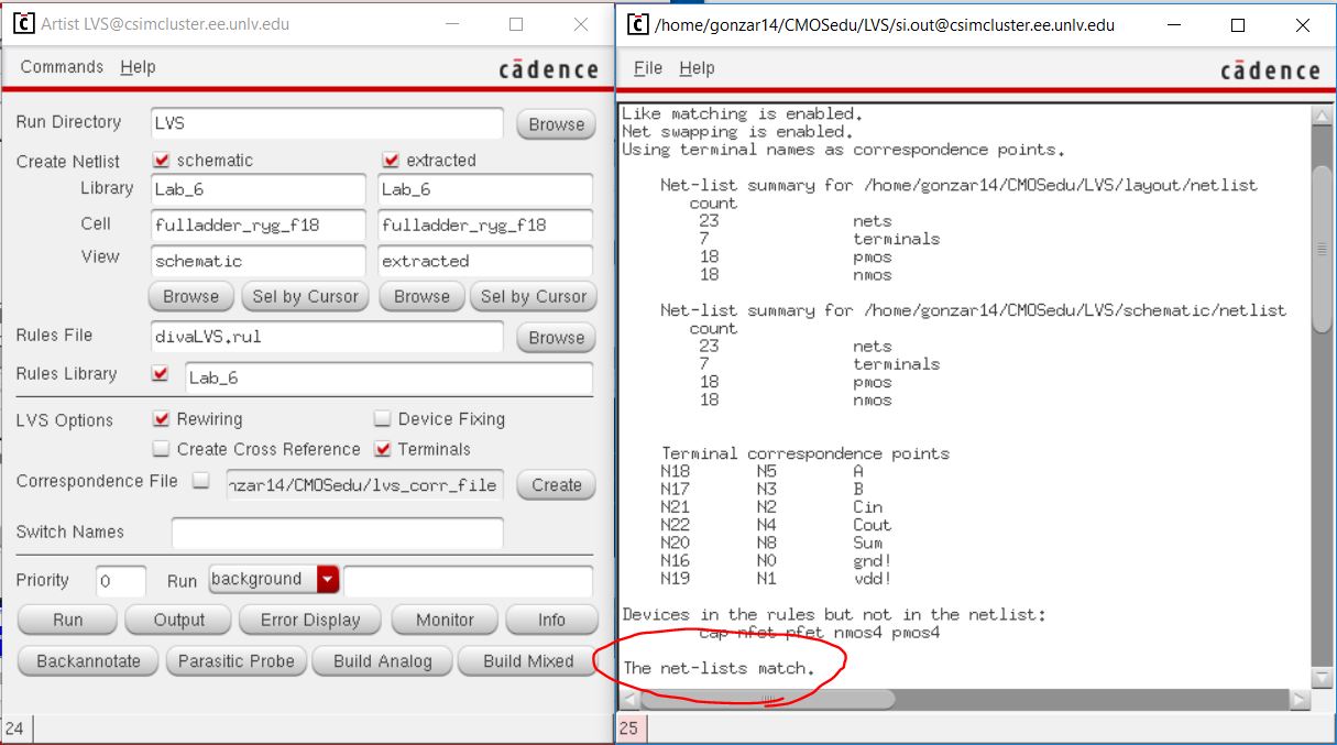
Simulate, using Spectre, the operation of the full-adder using this symbol. DRC and LVS your full adder design.
| Full-adder Schematic | Full-adder Layout |
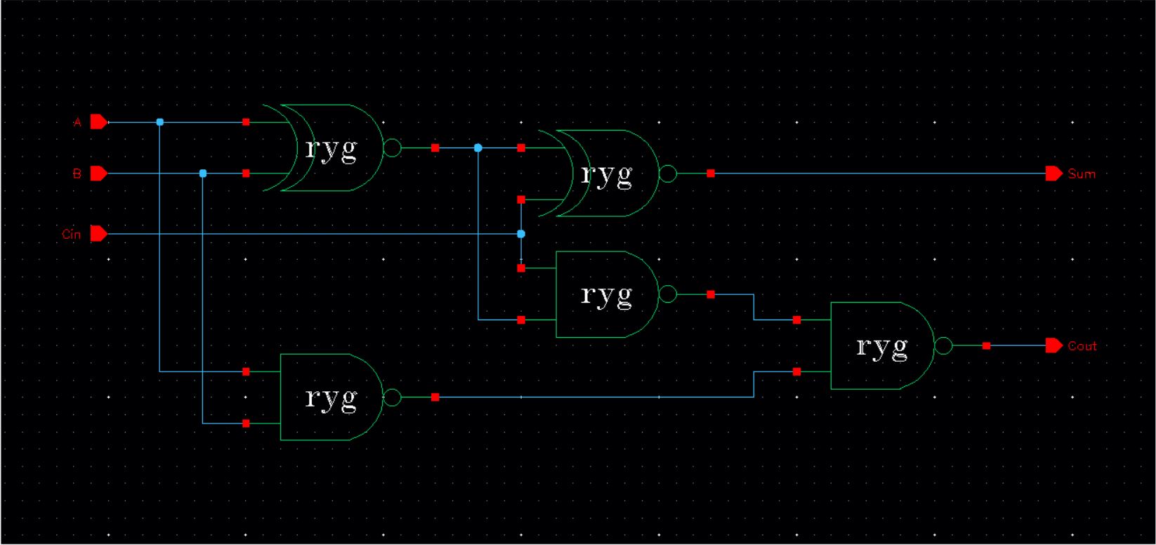 | 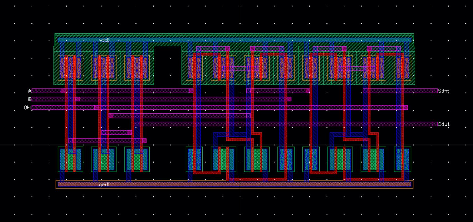 |
| Full-Adder Extracted | Full-adder Symbol |
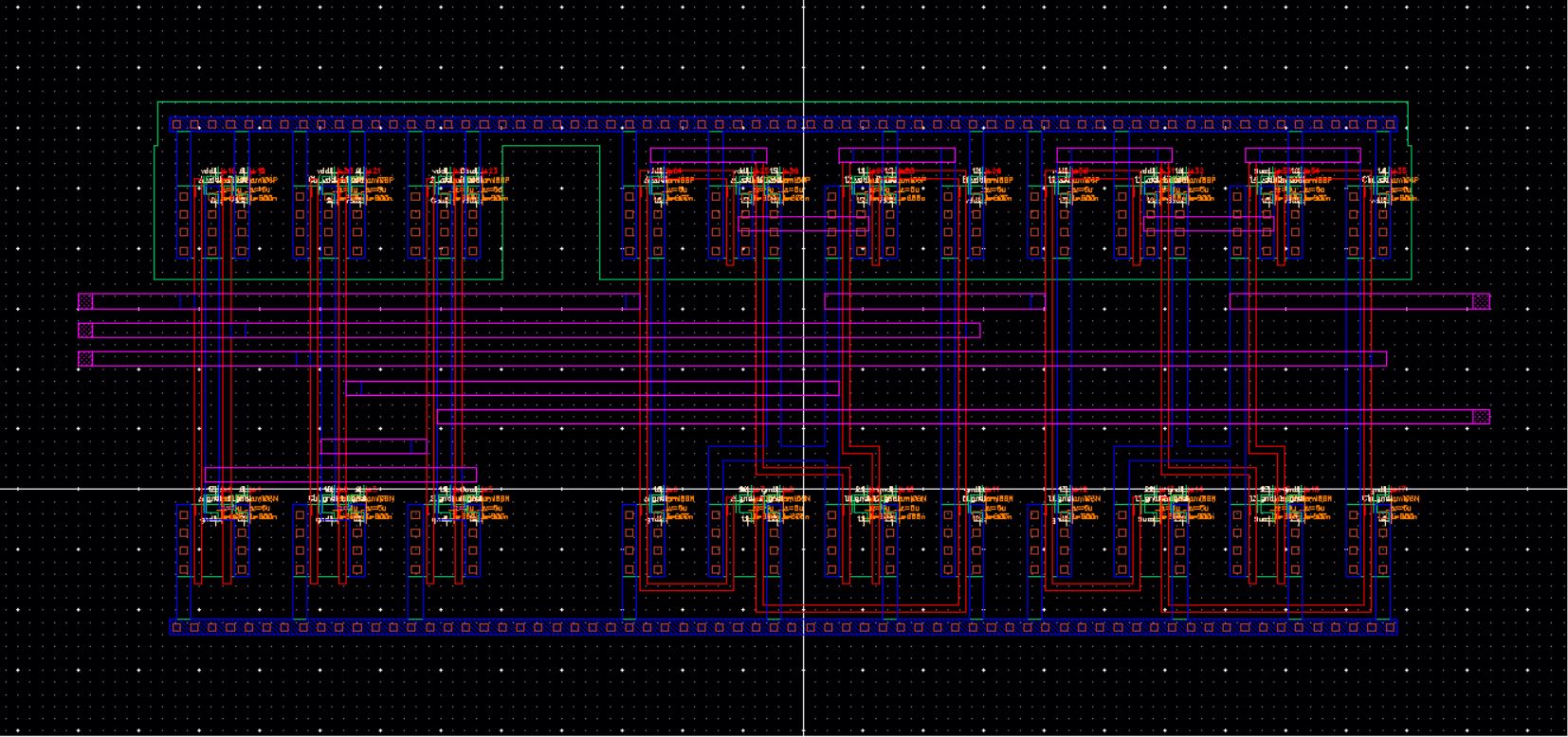 | 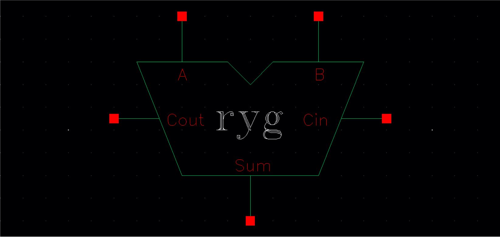 |
The following images indicate that the DRC/LVS of the Layout for the XOR logic gate had no errors.
Step 4: Simulate, using Spectre, the operation of the full-adder using this symbol.
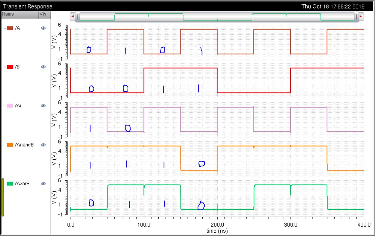
| Gate Simulation Schematic | Gate Outputs |
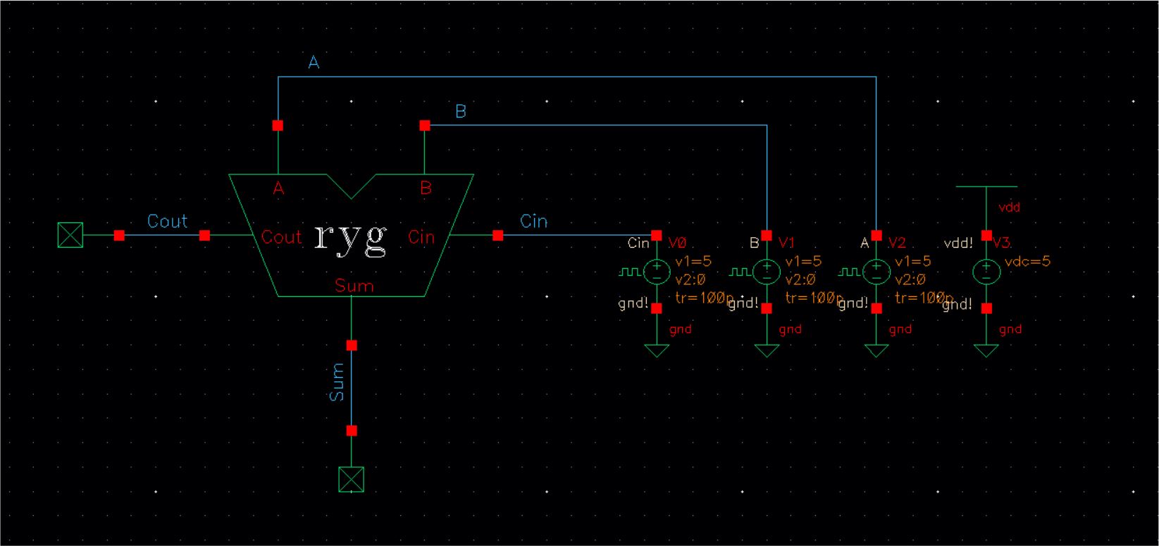 | 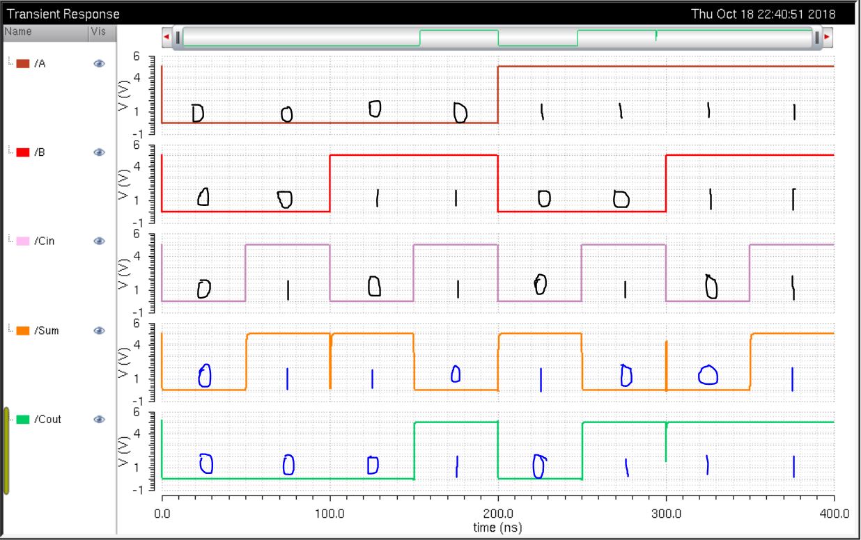 |
We can note that the full-adder operates correctly based from the Truth Table directly below:
| A | B | Cin | Sum | Cout | |
| 0 | 0 | 0 | 0 | 0 | |
| 0 | 0 | 1 | 1 | 0 | |
| 0 | 1 | 0 | 1 | 0 | |
| 0 | 1 | 1 | 0 | 1 | |
| 1 | 0 | 0 | 1 | 0 | |
| 1 | 0 | 1 | 0 | 1 | |
| 1 | 1 | 0 | 0 | 1 | |
| 1 | 1 | 1 | 1 | 1 |
----------------------------------------------------------------------------------------------------
The design directory is downloaded from the MobaXterm server and backed up onto this website (Up-to-date 10/24/18).
-> They are stored into my backup folder on my laptop and also on my online drive.
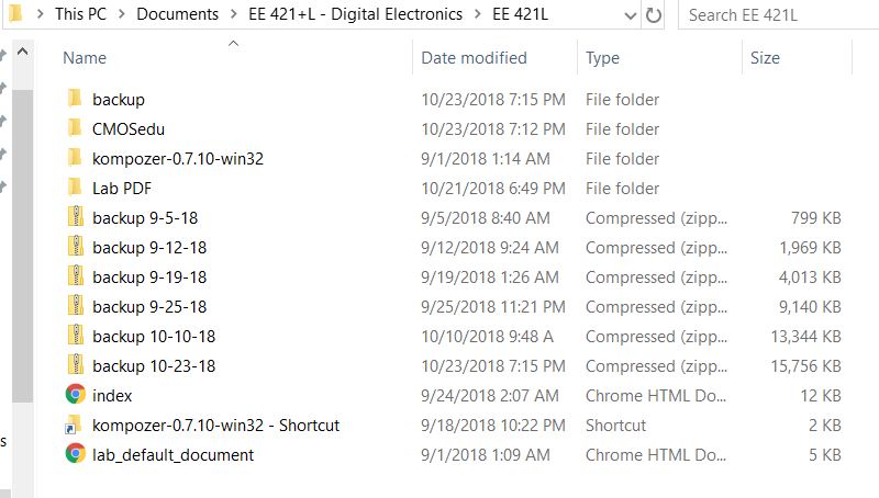
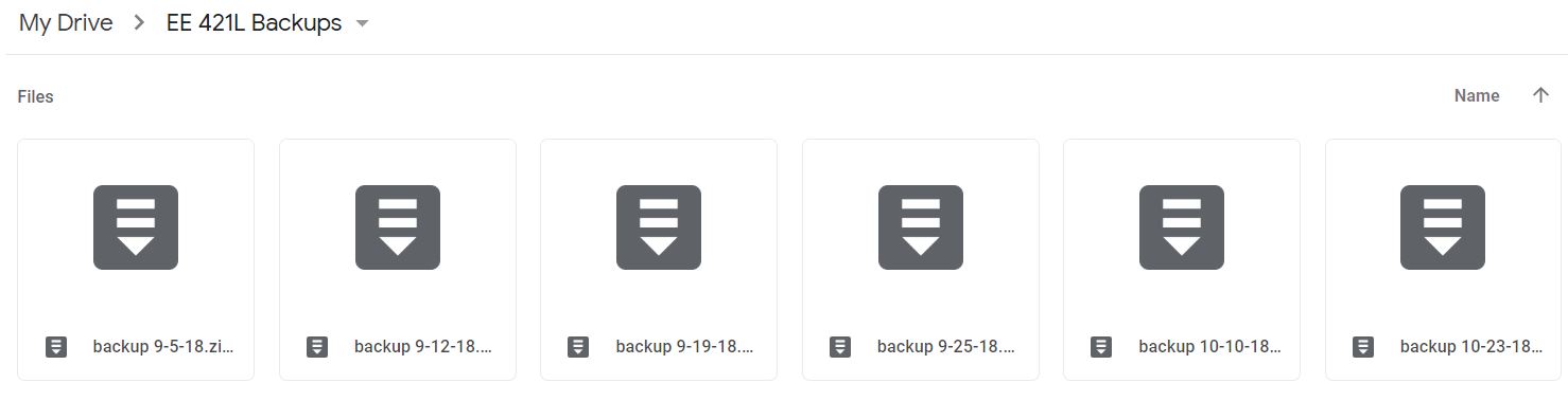
The CMOSedu directory has been backed up, and my following lab design directories will be continued to become backe up.
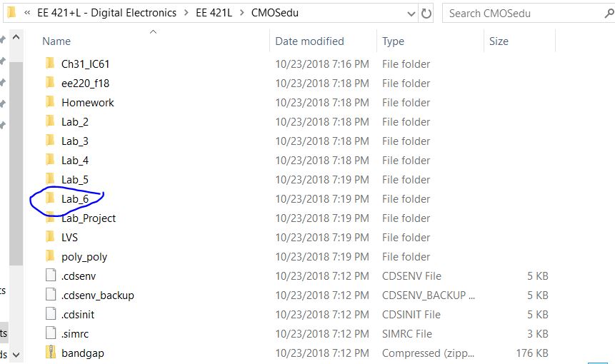
Lab_6 is circled to indicate the backup onto my computer.
The Lab_6 files are shared and can be downloaded by this 'link'.
----------------------------------------------------------------------------------------------------
This Concludes the Lab 6 Report.