Lab 05 - EE 421L
----------------------------------------------------------------------------------------------------
Prelab:
The labs are backed up through a saved directory in my computer as well as into my google drive account (Up-to-Date from end of previous lab).
The
prelab also demonstrates Tutorial 3 on the CMOSedu website. The image
size can be increased by clicking on the images for more detail.
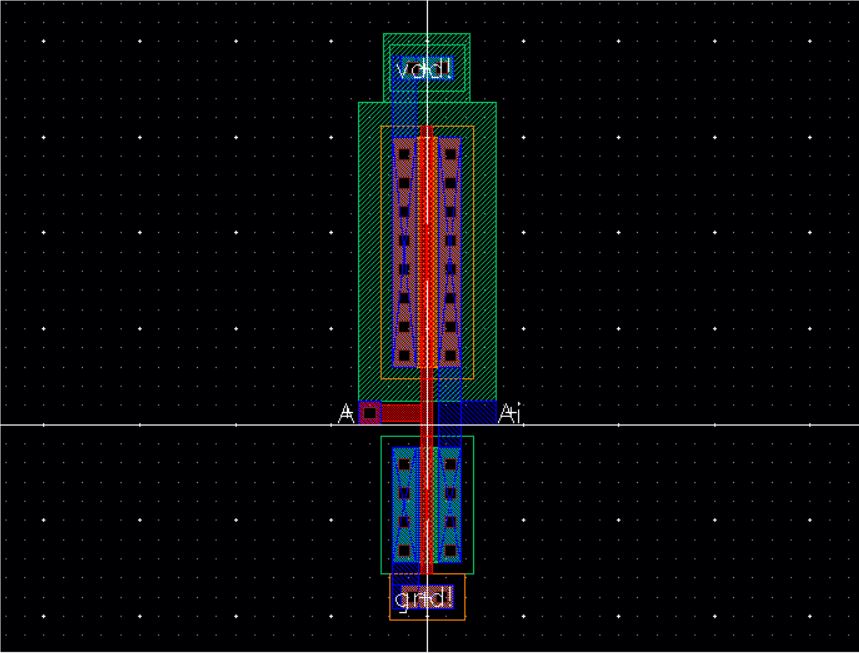
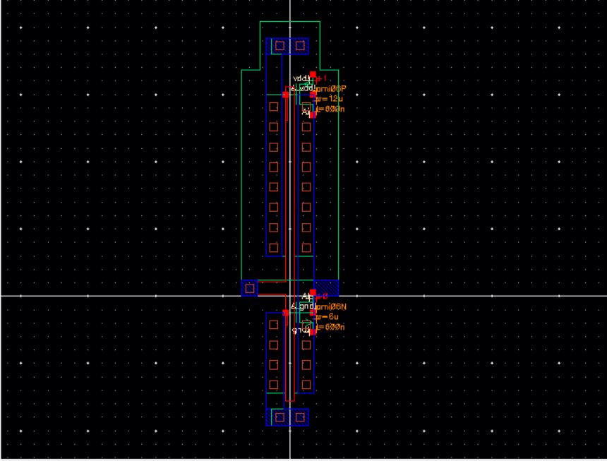
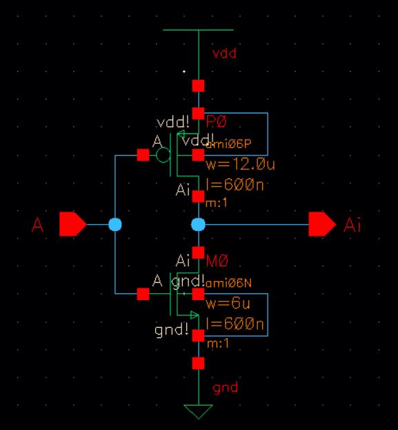
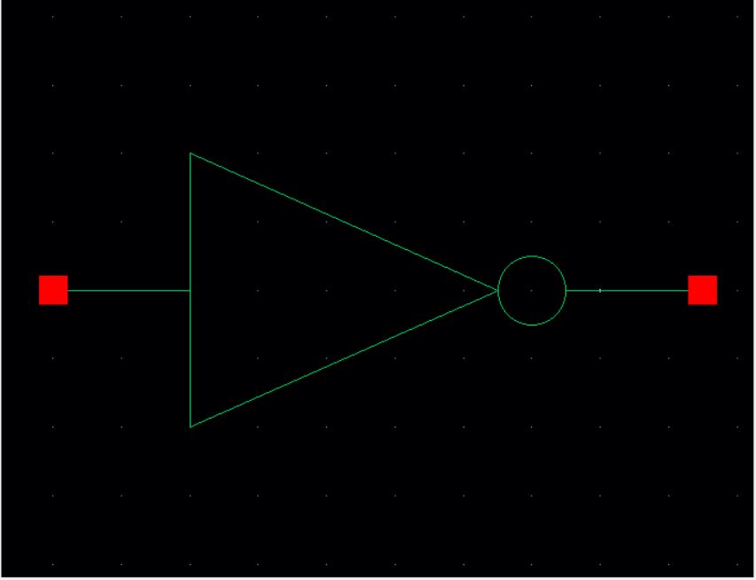
| Inverter Layout | Inverter Extraction | Inverter Schematic | Inverter Symbol |
|
|
|
|
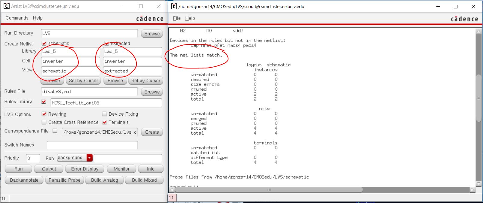
The following demonstrates an LVS:
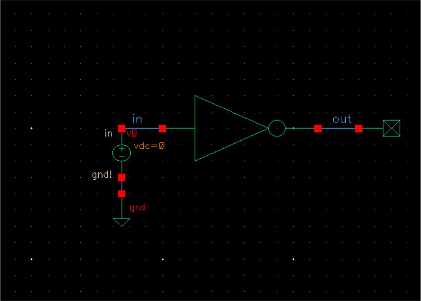
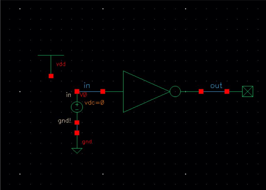
Setting up an Inverter Schematic:
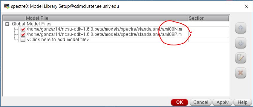
Attaching model libraries for a NMOS and PMOS:
Simulation Analysis:
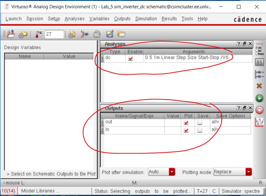
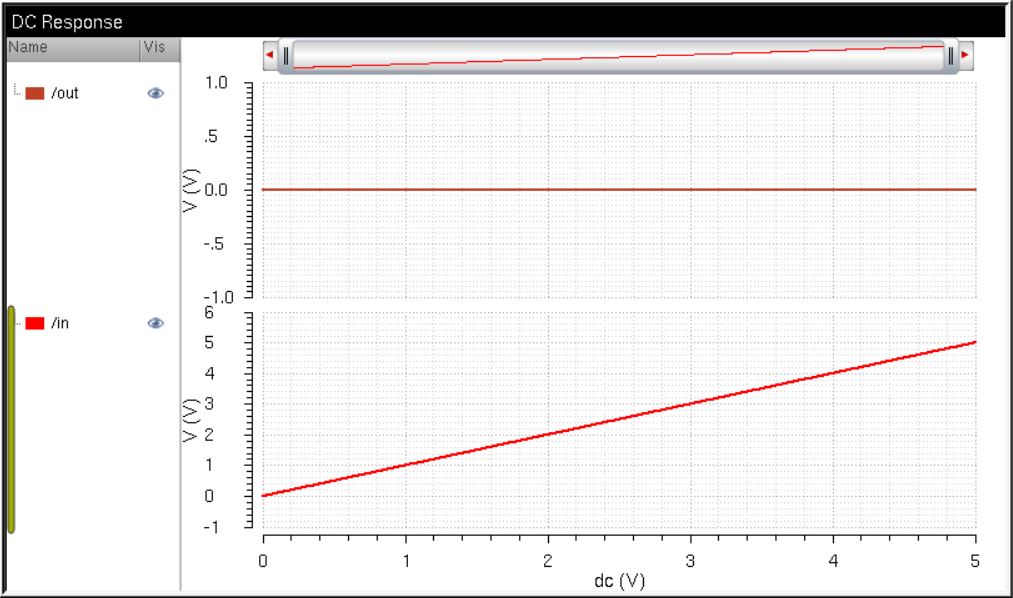
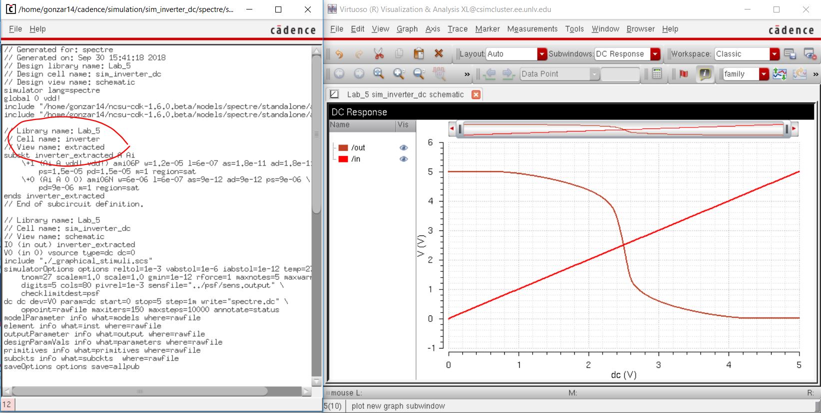
Output Results for Vin and Vout:
Adding a Vdd onto the schematic for proper LVS simulation:
LVS Simulation (extracted file utilized):
----------------------------------------------------------------------------------------------------
Lab:
The following lab will recycle the layout and schmatics from the Tutorial 3 and be extended to demonstrate an inverter of greater NMOS/PMOS dimensions.
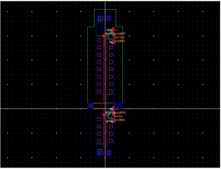
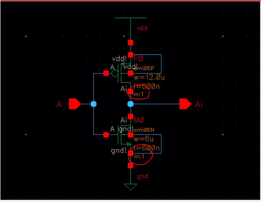
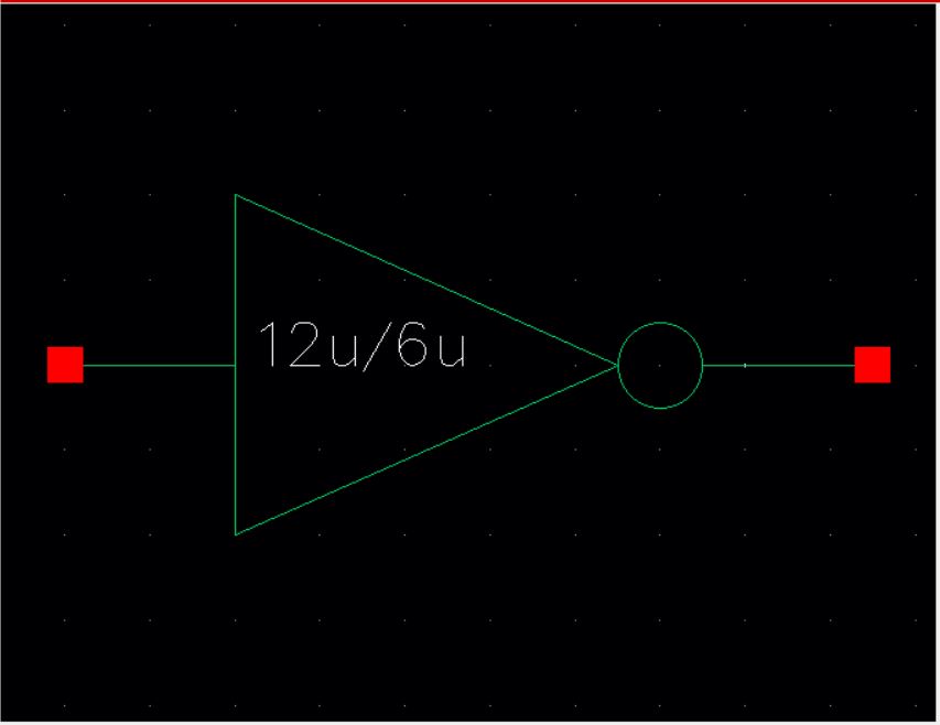
Step 1: Draft schematics, layouts, and symbols for two inverters having sizes of:
| Inverter Layout | Inverter Extraction | Inverter Schematic | Inverter Symbol |
 |
 |
 |
 |
| Inverter Layout | Inverter Extraction | Inverter Schematic | Inverter Symbol |
 |
 |
 |
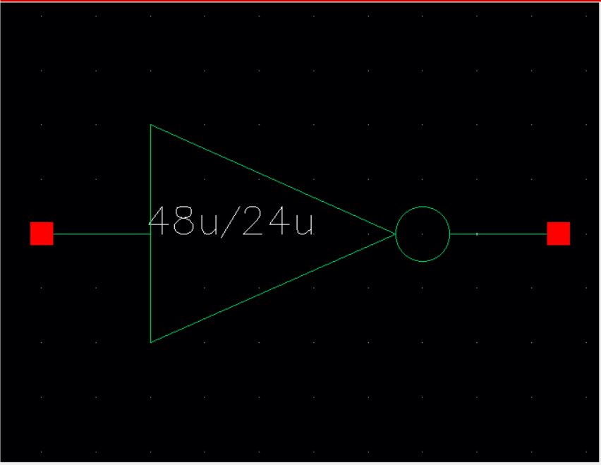 |
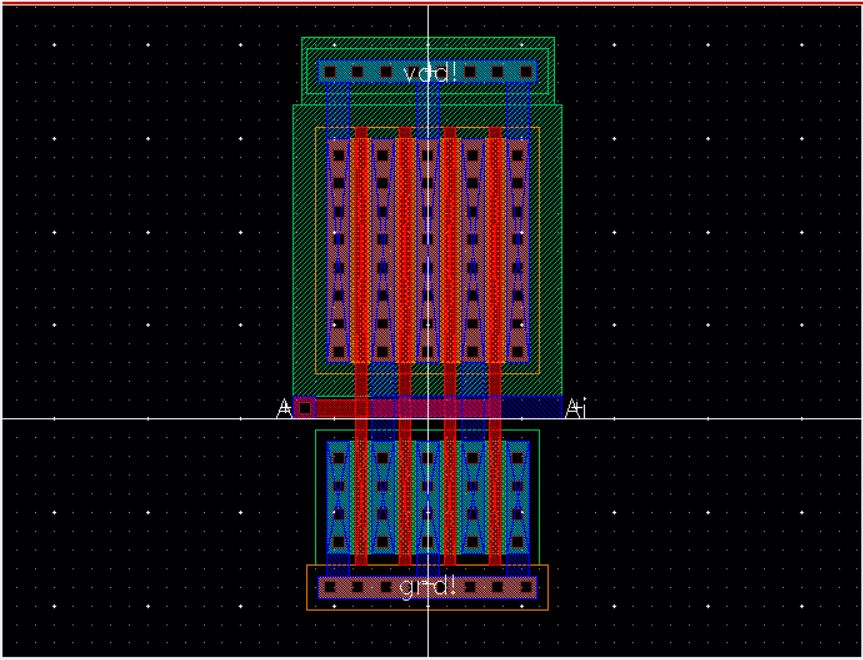
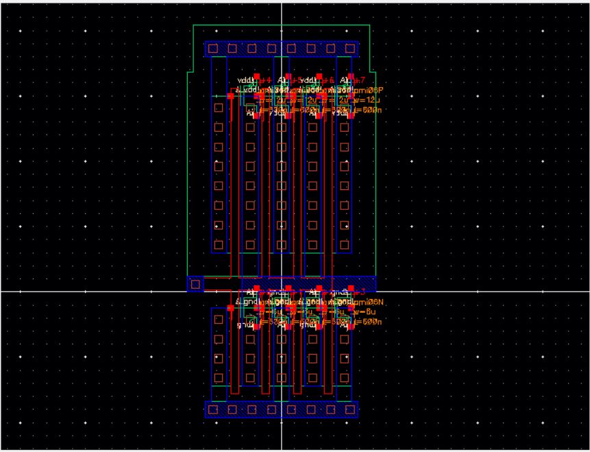
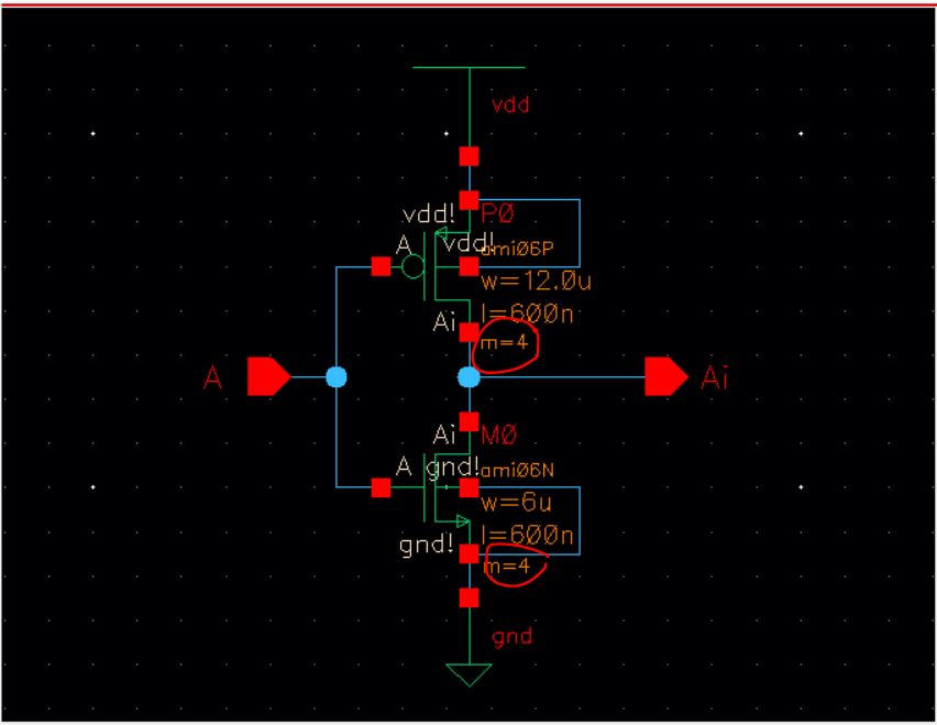
Following similarly to the previous inverter configuration, the only change is the increase in dimensions for the inverter. The dimensions are increased by adding more fingers to the layout. The principle of the inverter acts the same as the previous.
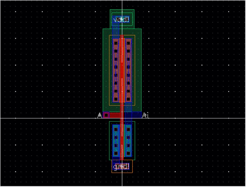
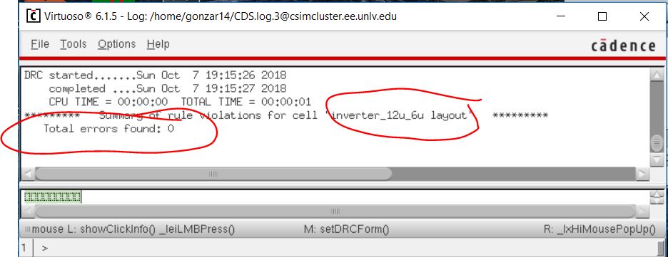
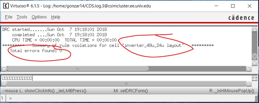
The
layout passes DRC guidelines as shown
below:
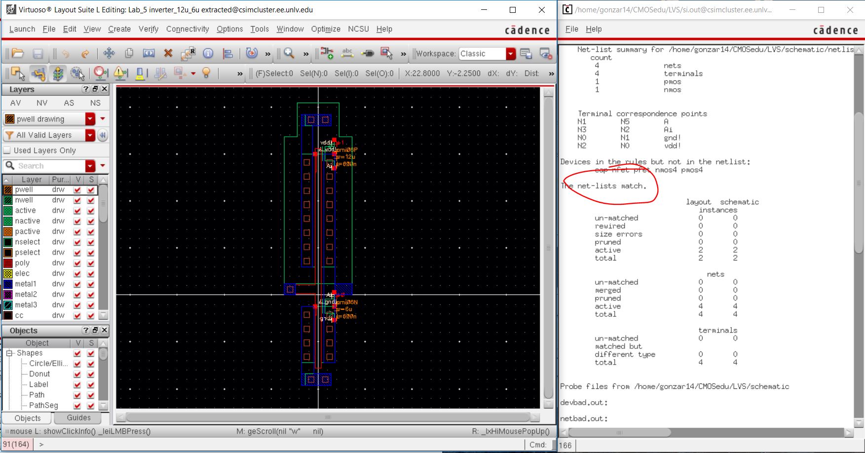
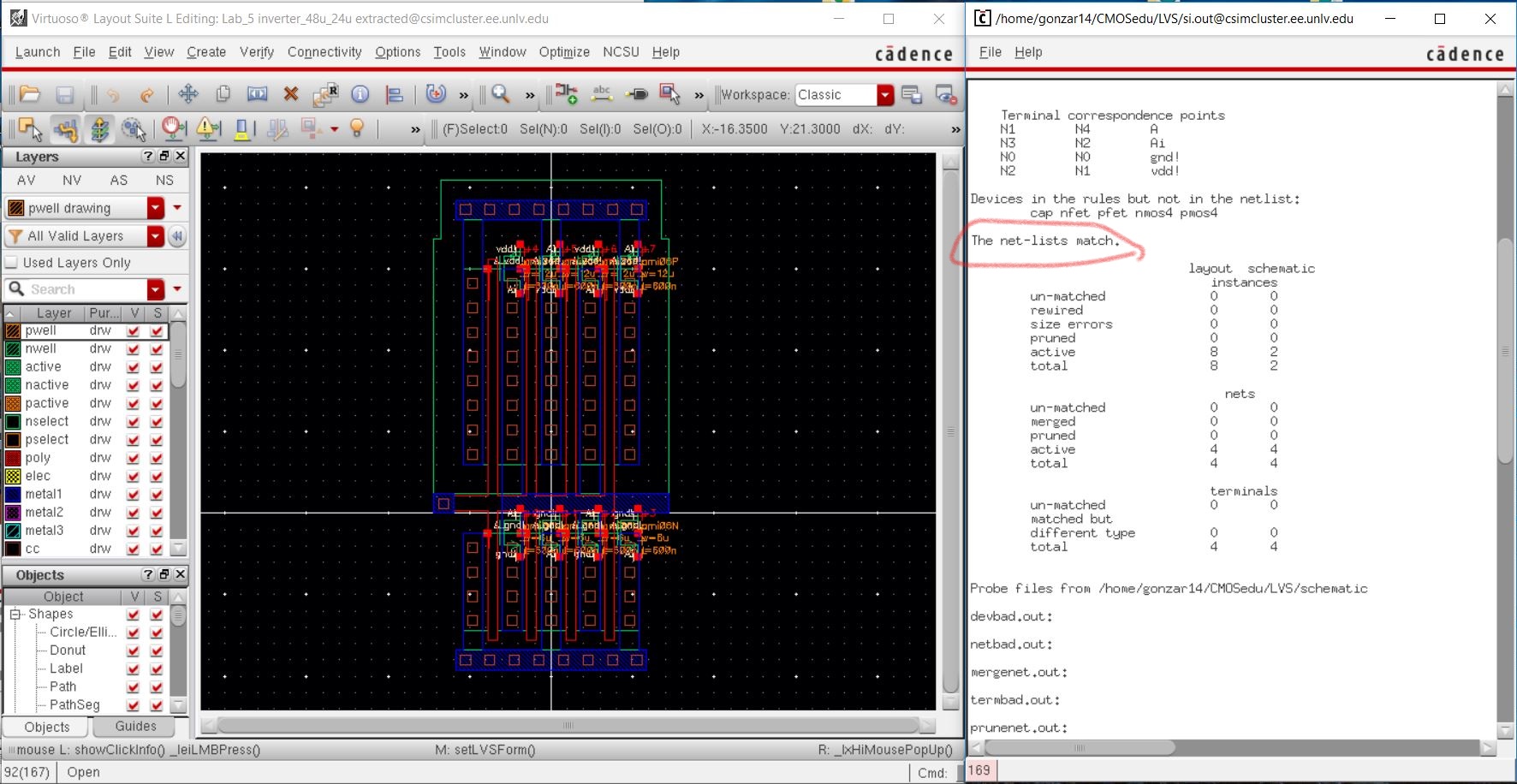
Comparing
the extracted layout with the schematic, we can see the CMOS
successfully matches through an LVS:
The files for the layout and schematics can be downloaded by clicking here: lab5_ryg.
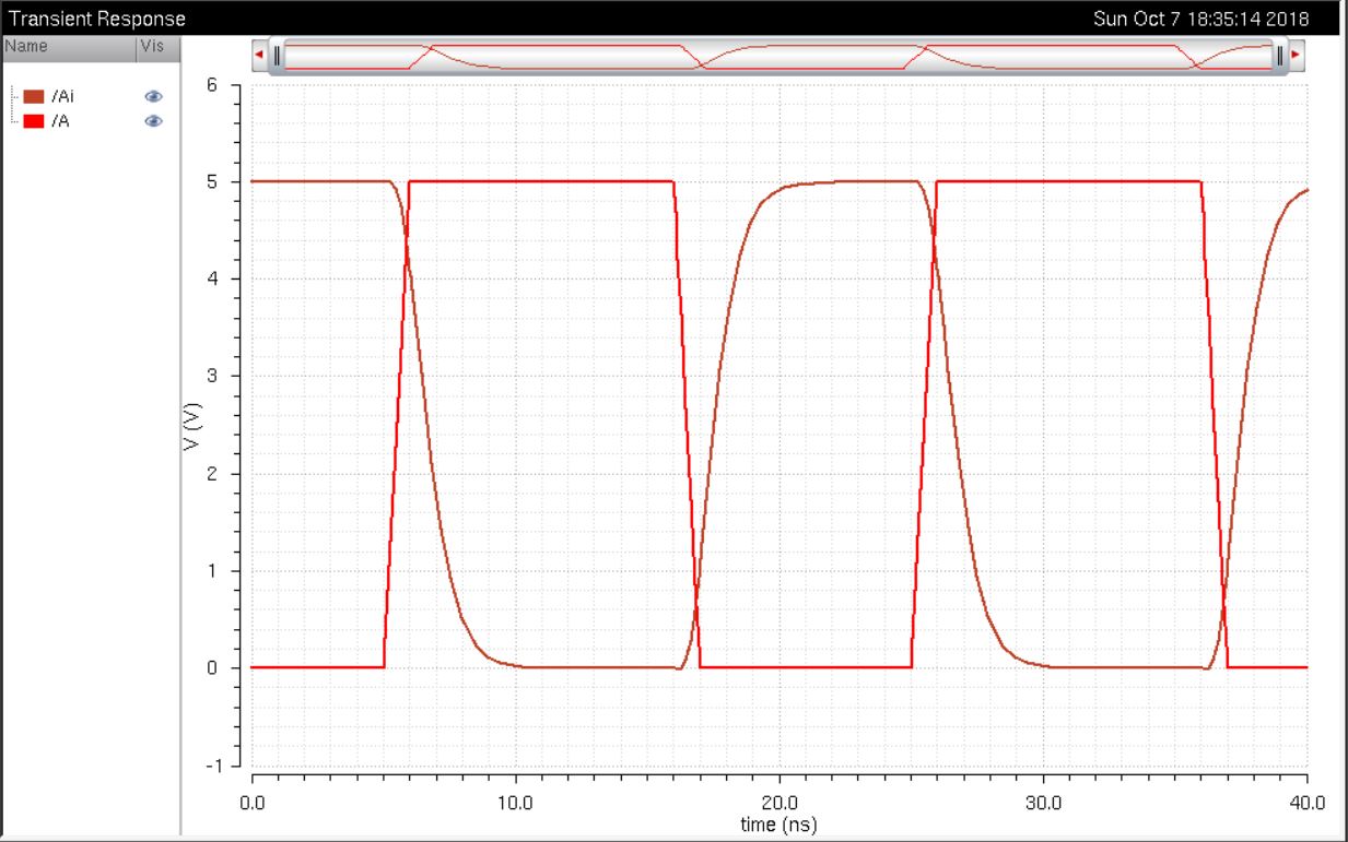
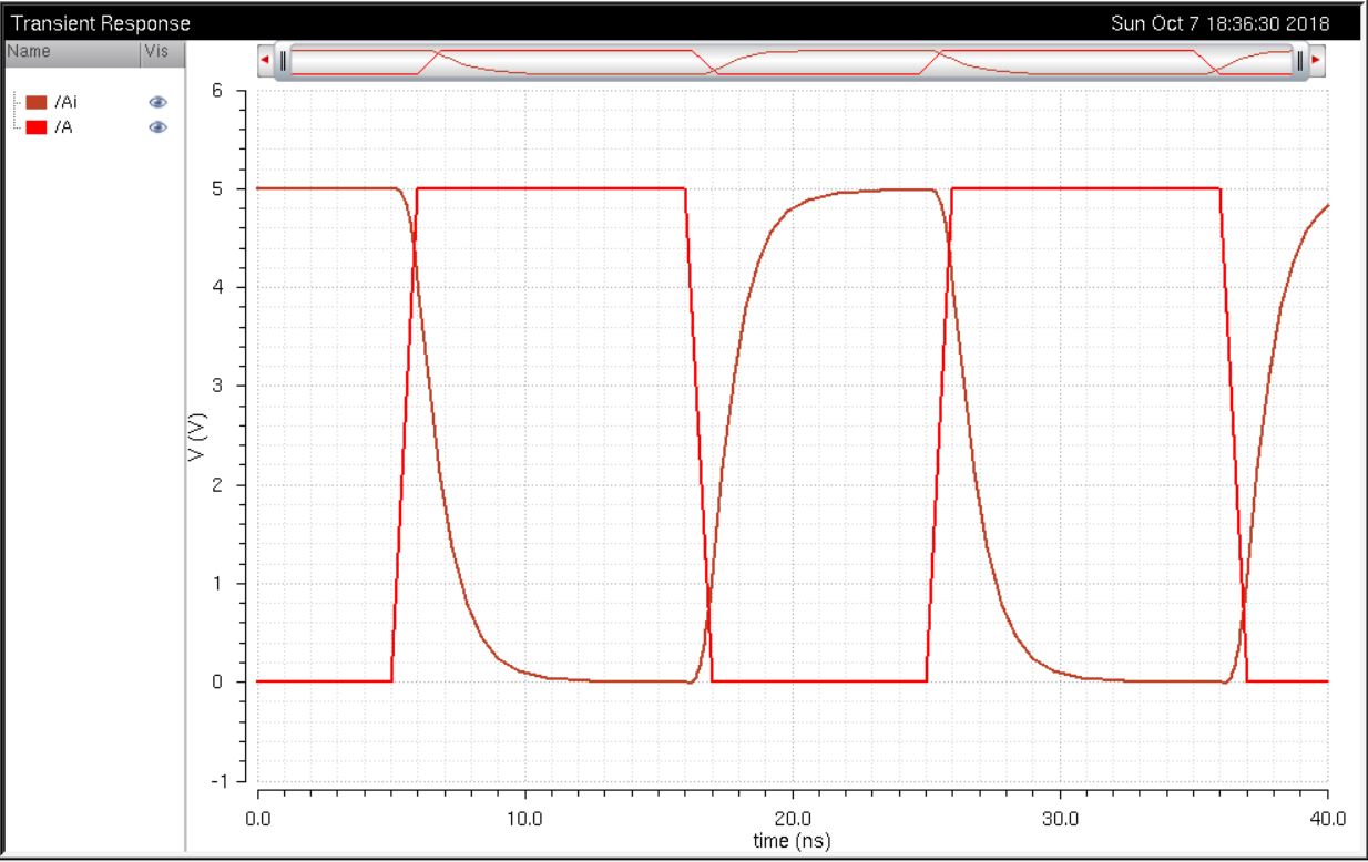
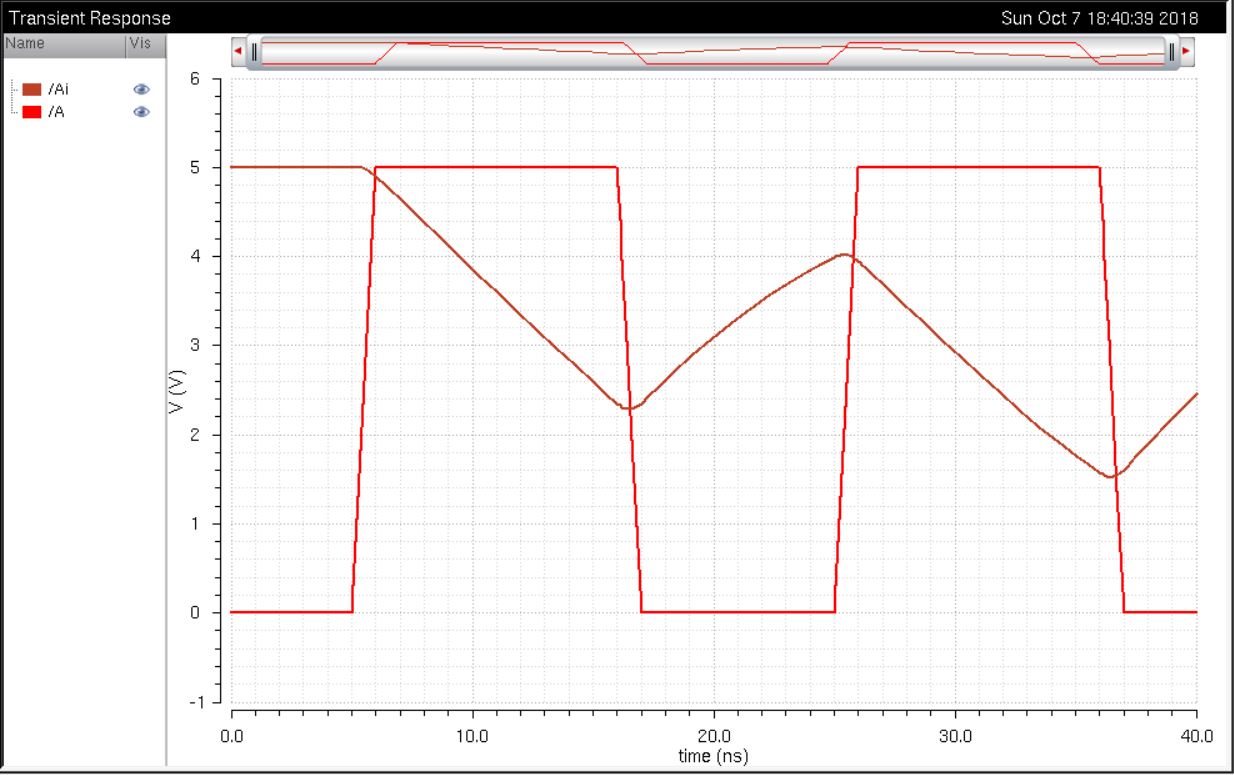
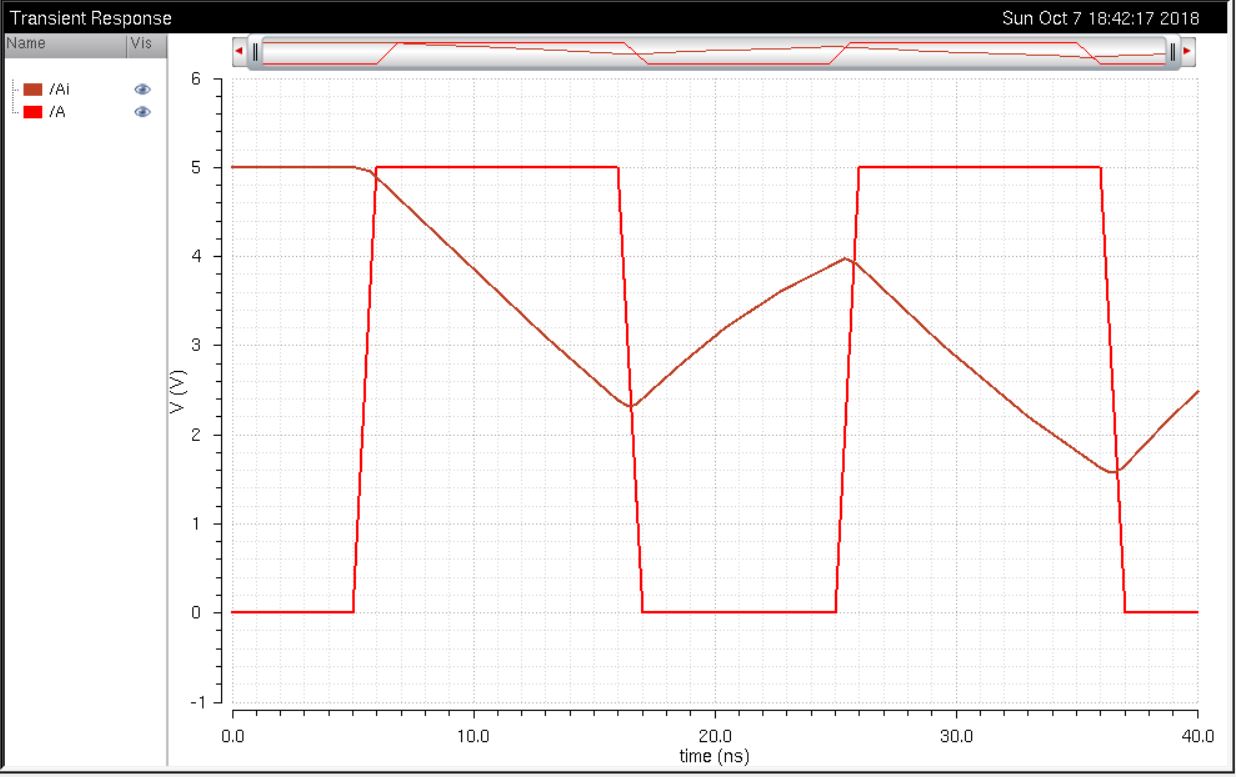
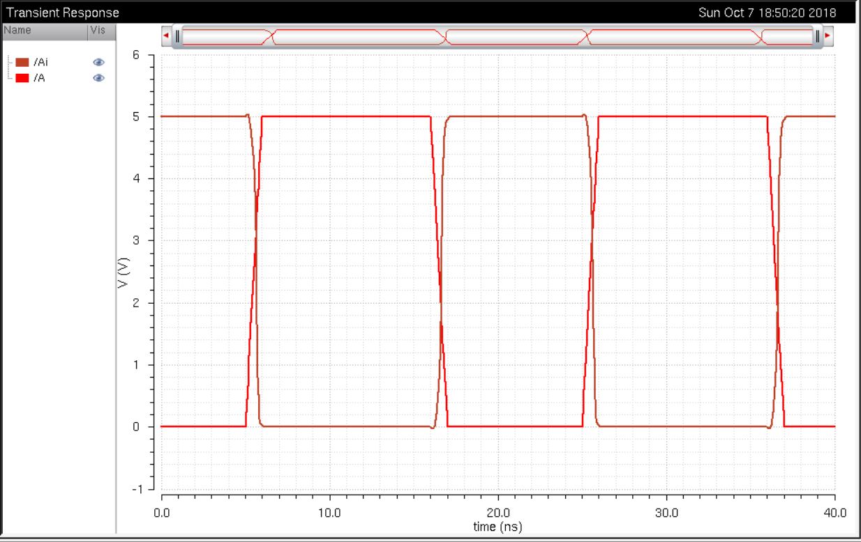
| Capacitance | Schematic | Spectre Output | UltraSim Output |
| 100fF | 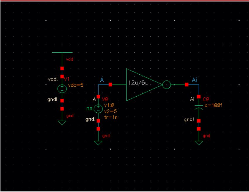 |
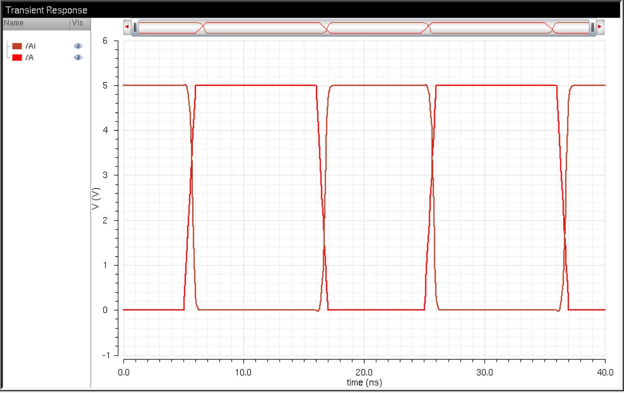 |
 |
| 1pF | 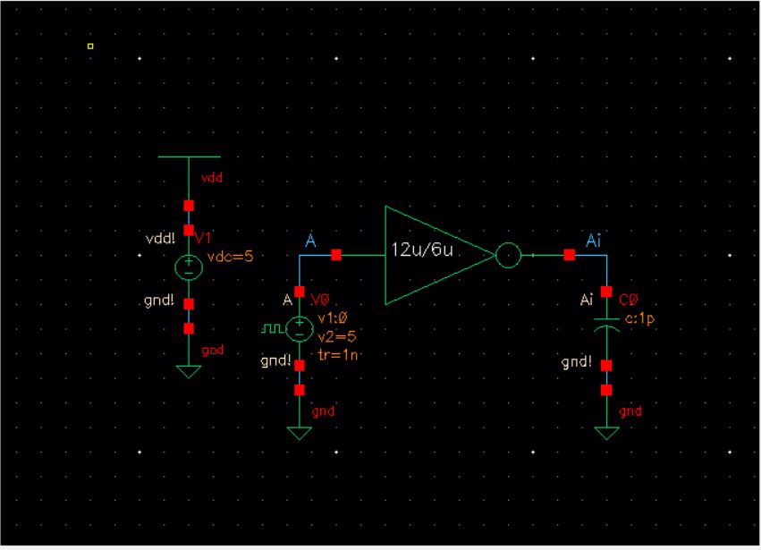 |
 |
 |
| 10pF | 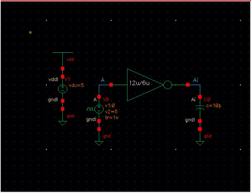 |
 |
 |
| 100pF | 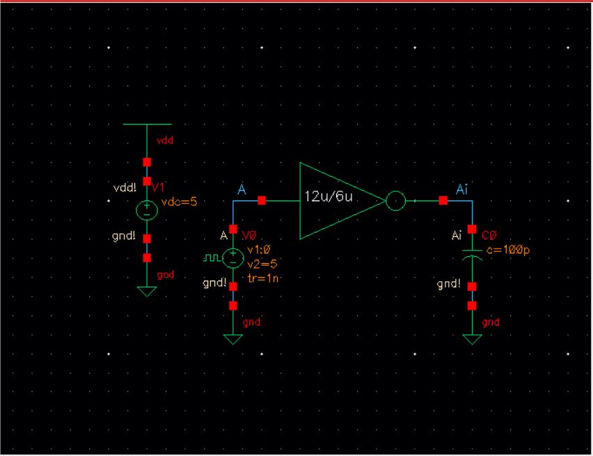 |
 |
 |
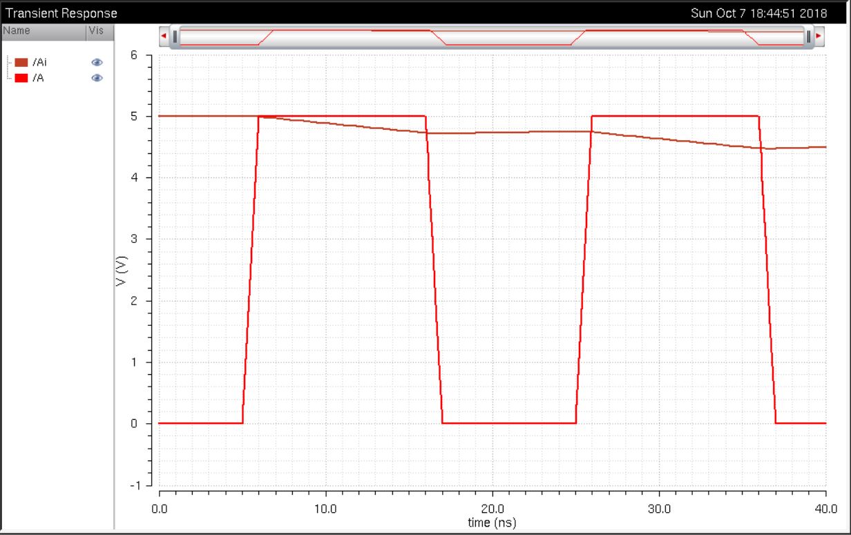
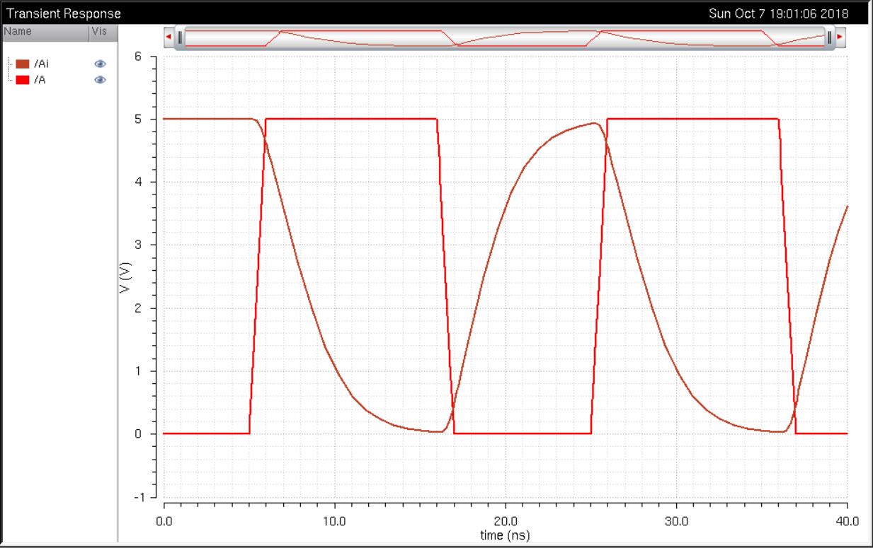
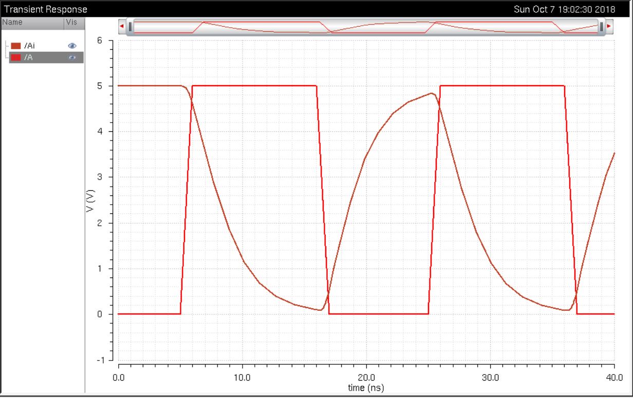
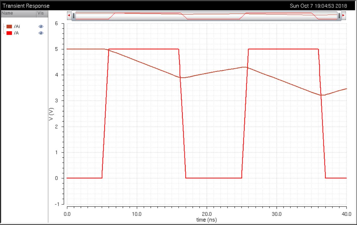
We can note that as the load capacitance is increased, the time it takes to charge the capacitor at the output is longer in response to change in the voltage input.
This can be fixed by minimizing the capacitive load or by decreasing the frequency signal. We can also note that there are slight variations between Spectre and UltraSim. UltraSim was the faster tool in regards to simulating the output.
Step 3: Use UltraSim (Cadence's fast SPICE simulator for larger circuits at the cost of accuracy) and repeat the above simulations.
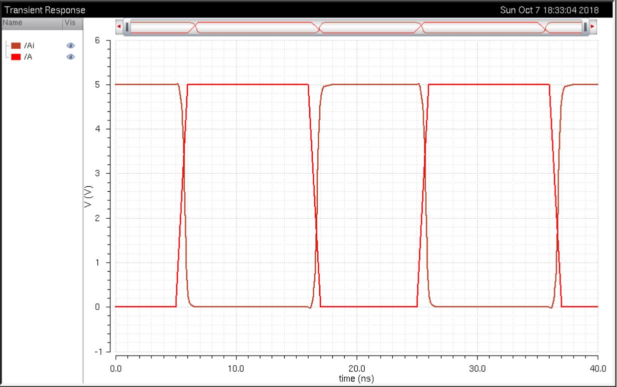
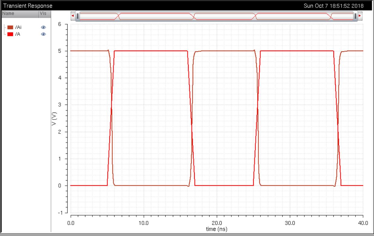
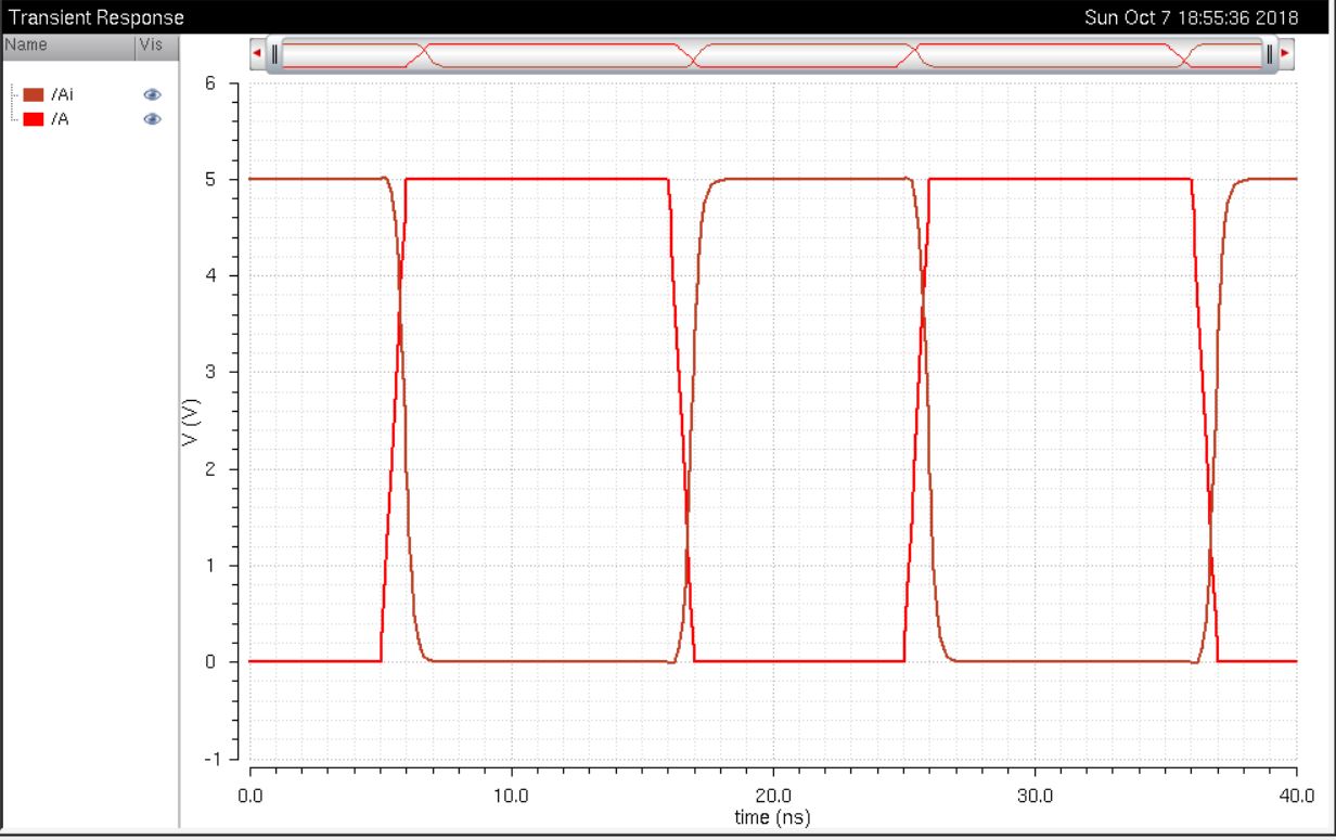
| Capacitance | Schematic | Spectre Output | UltraSim Output |
| 100fF | 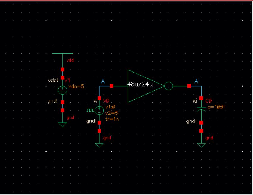 |
 |
 |
| 1pF | 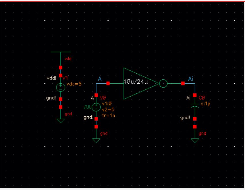 |
 |
 |
| 10pF | 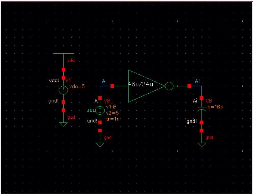 |
 |
 |
| 100pF | 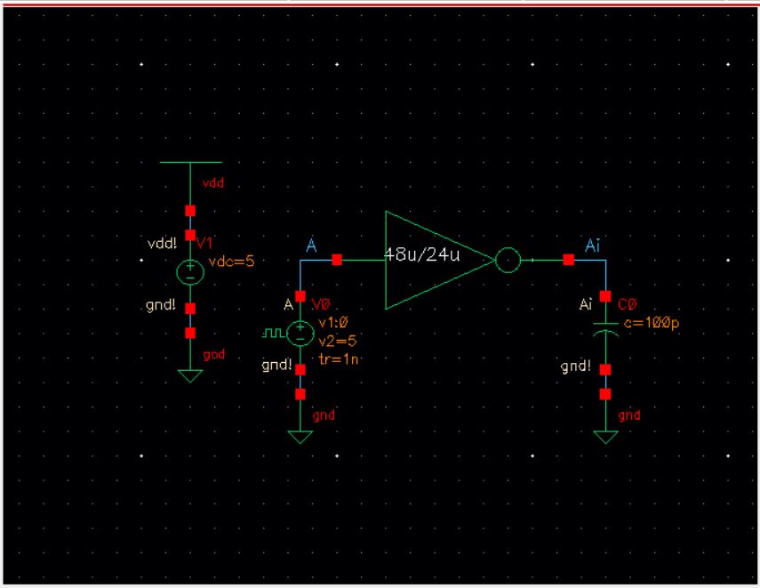 |
 |
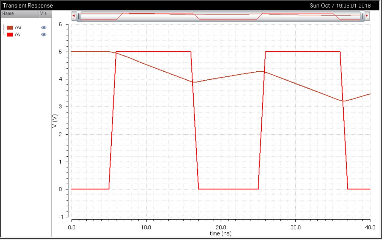 |
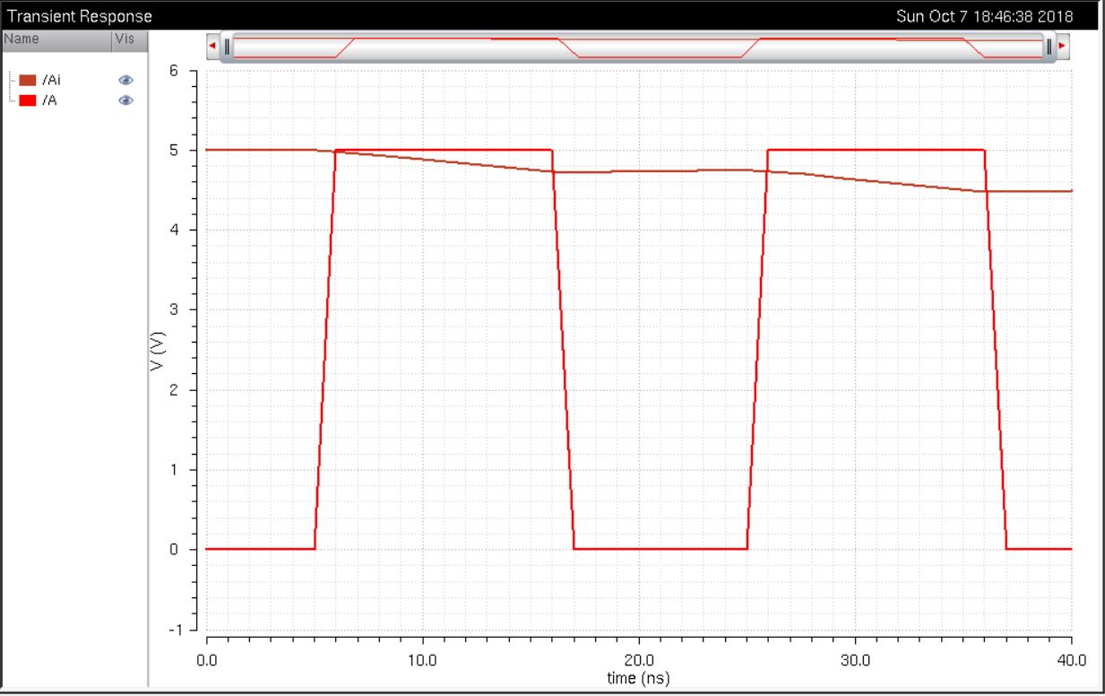
Compared to the previous inverter, we can note that the 48u/24u is able to handle larger capacitive loads. Likewise, there is slight variation between Spectre and UltraSim except that UltraSim runs a lot faster compared to Spectre.
----------------------------------------------------------------------------------------------------
The design directory is downloaded from the MobaXterm server and backed up onto this website (Up-to-date 10/10/18).
-> They are stored into my backup folder on my laptop and also on my online drive.
----------------------------------------------------------------------------------------------------
This Concludes the Lab 5 Report.