Lab 04 - EE 421L
----------------------------------------------------------------------------------------------------
Prelab:
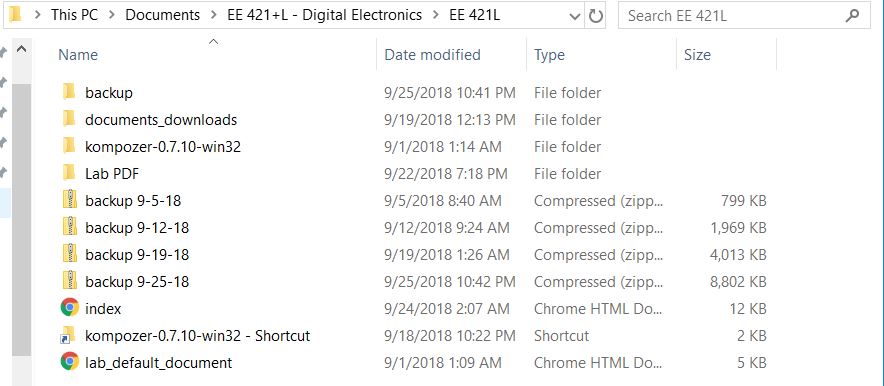
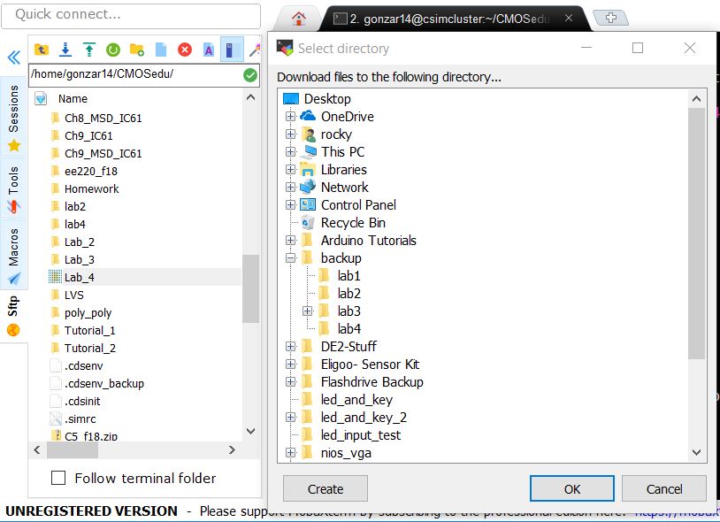
The labs are backed up through a saved directory in my computer as well as into my google drive account:
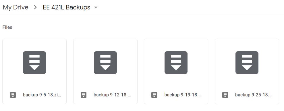
We can note that if memory space was limited, we could delete the oldest backups and keep the most recent.
But since we have a lot of free memory, we'll just keep every backup.
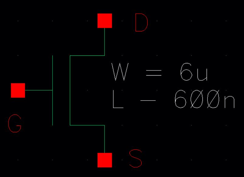
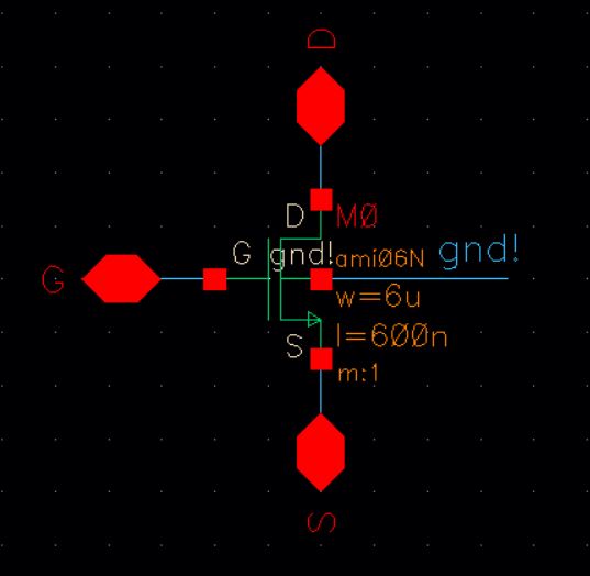
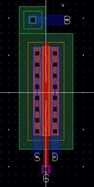
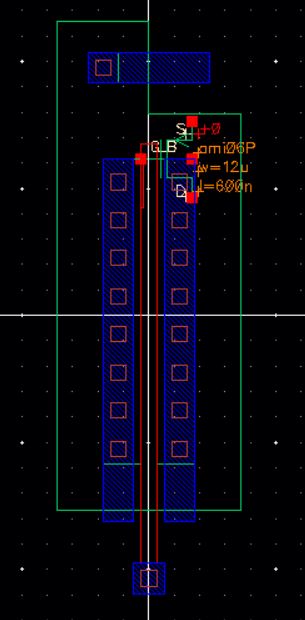
In Tutorial 2, an NMOS and PMOS layout/schematic are designed. The components follow:
| NMOS/PMOS Layout | NMOS/PMOS Extraction | NMOS/PMOS Symbol | NMOS/PMOS Schematic |
 |  |  |  |
 |  |  |  |
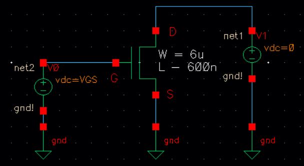
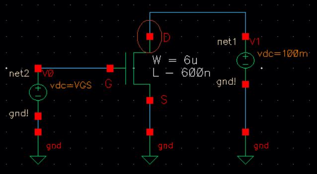
For Simulation purposes, the following schematic for an NMOS was used:
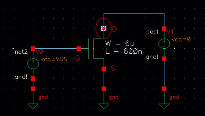
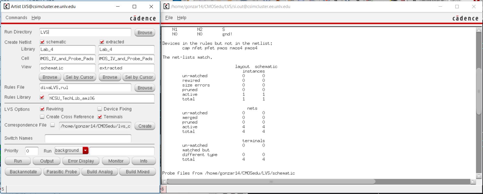
Since the layout and schemactic exist for the NMOS, an LVS is preformed, and the extraction is used for the schematic:

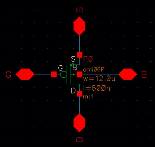
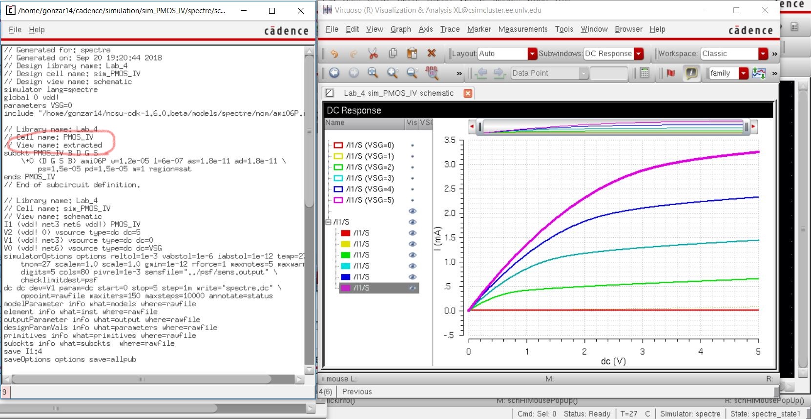
For Simulation purposes, the following schematic for an PMOS was used:
Since the layout and schemactic exist for the PMOS, an LVS is preformed, and the extraction is used for the schematic:
----------------------------------------------------------------------------------------------------
Lab:
Step 1: Generate the following 4 schematics and simulations.
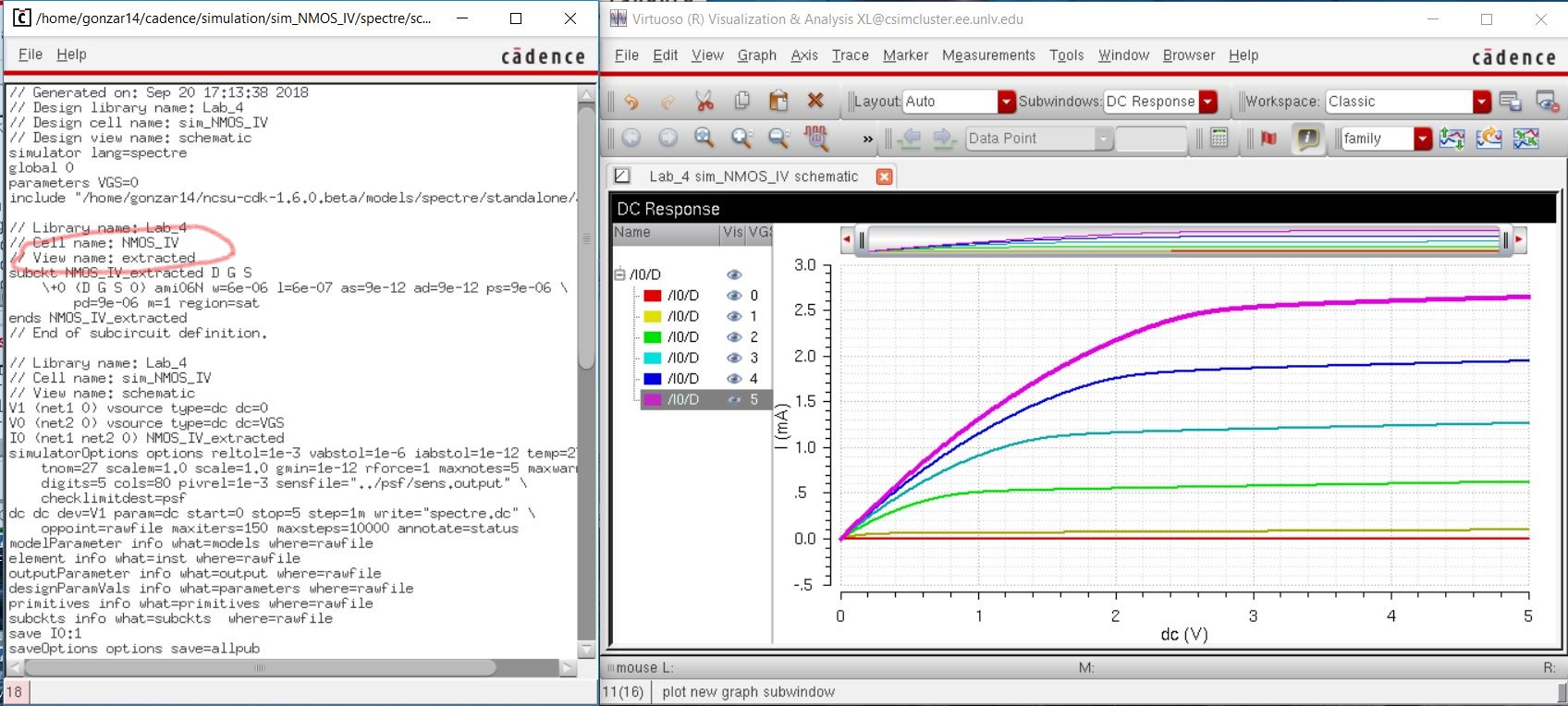
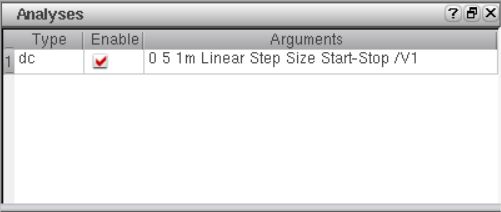
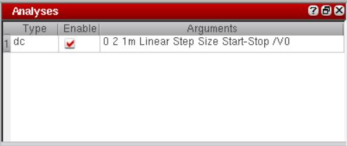
| *Note that VGS is variating instantaneously from '0V - 5V'; VDS is variating from '0V - 5V' for Linear Steps of '1'. | |
 | 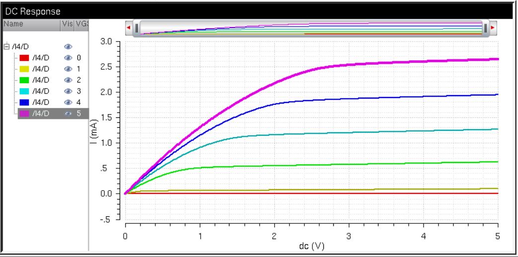 |
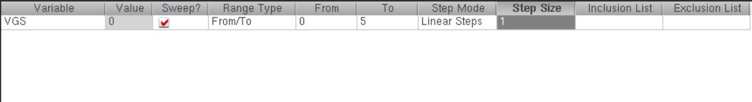
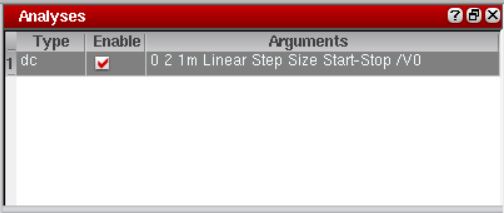
| *Note that VGS is variating instantaneously from '0V - 2V'; VDS is held constant at 100mV. | |
 | 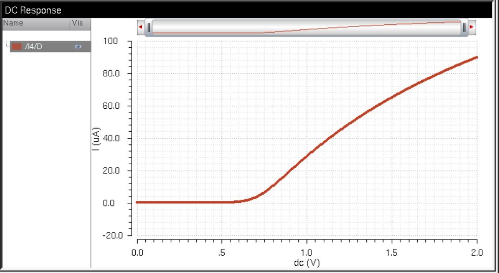 |
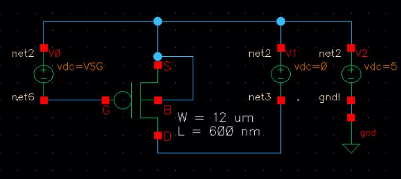
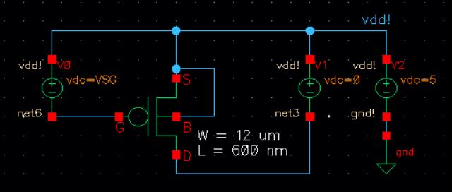
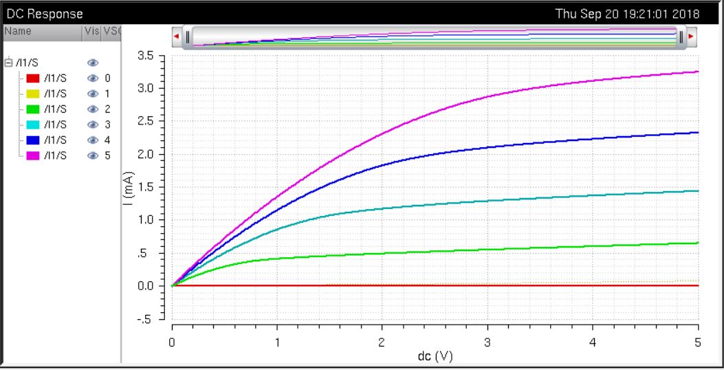
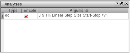
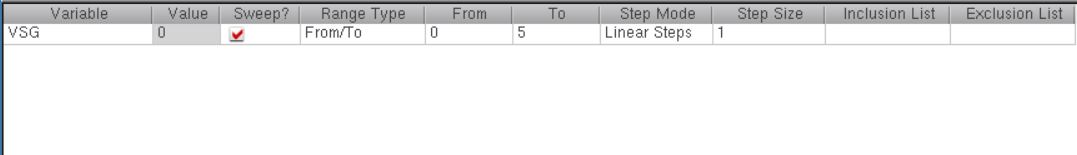
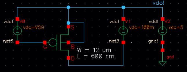
| *Note that VSG is variating instantaneously from '0V - 5V'; VSD is variating from '0V - 5V' for Linear Steps of '1'. | |
 |  |
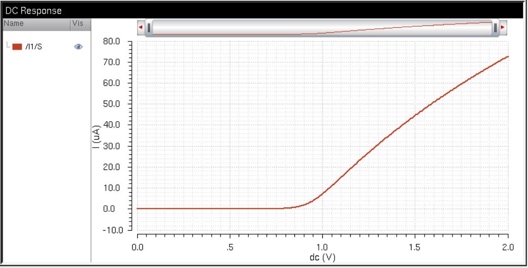
| *Note that VSG is variating instantaneously from '0V - 2V'; VSD is held constant at 100mV: | |
 |  |
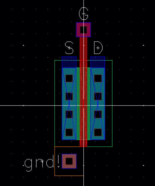
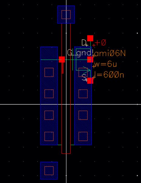
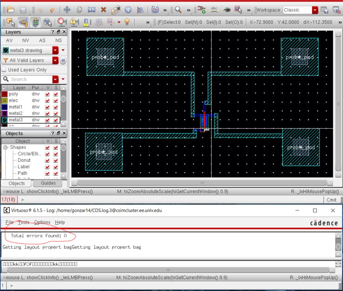
Step 2: Lay out a 6u/0.6u NMOS device and connect all 4 MOSFET terminals to probe pads (which can be considerably smaller than bond pads [see MOSIS design rules] and directly adjacent to the MOSFET (so the layout is relative small).
-> Since the parameters were already chosen and created into a Lay out during the prelab, we will just connect the NMOS device to probe pads.
-> A probe pad has a simple layout of 'glass' over 'metal3'.
-> The schematic i just an input/output pin since it provides physical connection to inside the chip.
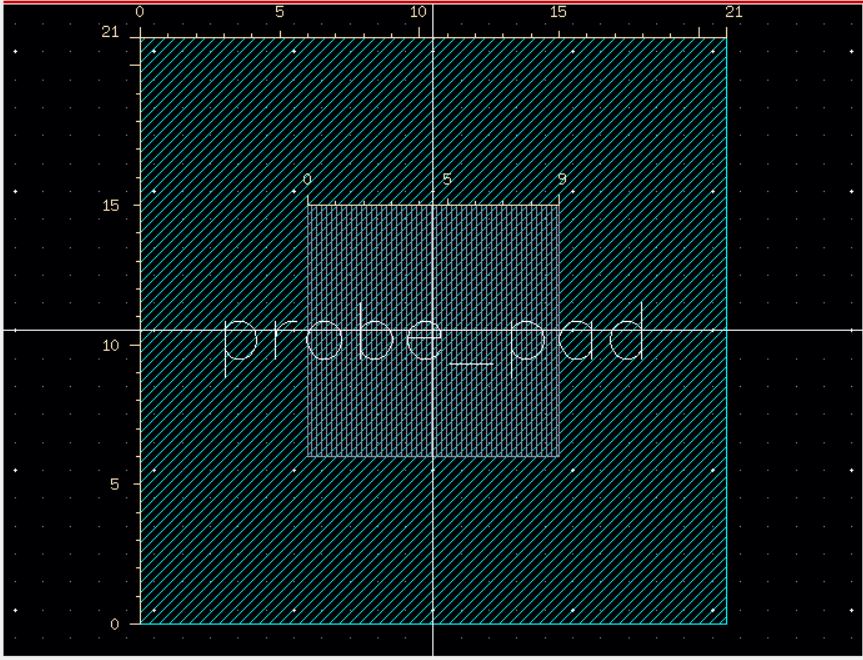 | 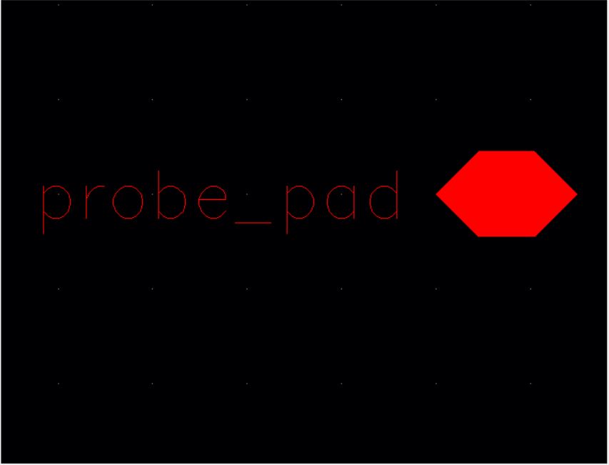 | 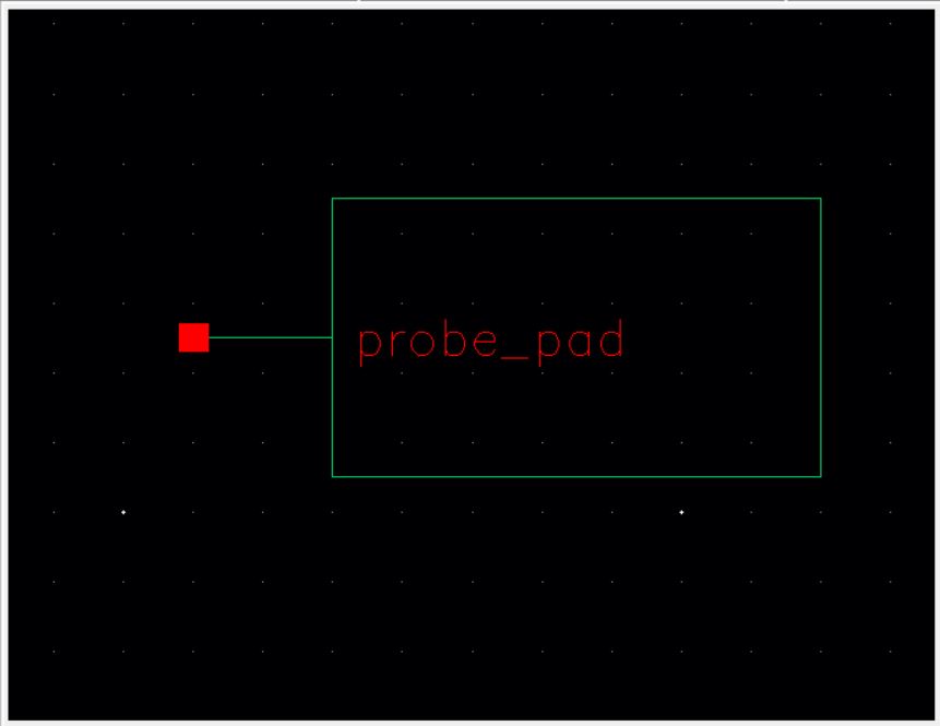 |
We can connect the probe_pads to each component of the NMOS (Drain, Source, Gate, Body).
However, since the metals are in different layers, we need to make sure the connections follow:
glass -> metal3 -> via2 -> metal2 -> via1 -> metal1 -> contact_cut
Then we can DRC the layout to make sure that there is enough distance between the different components.
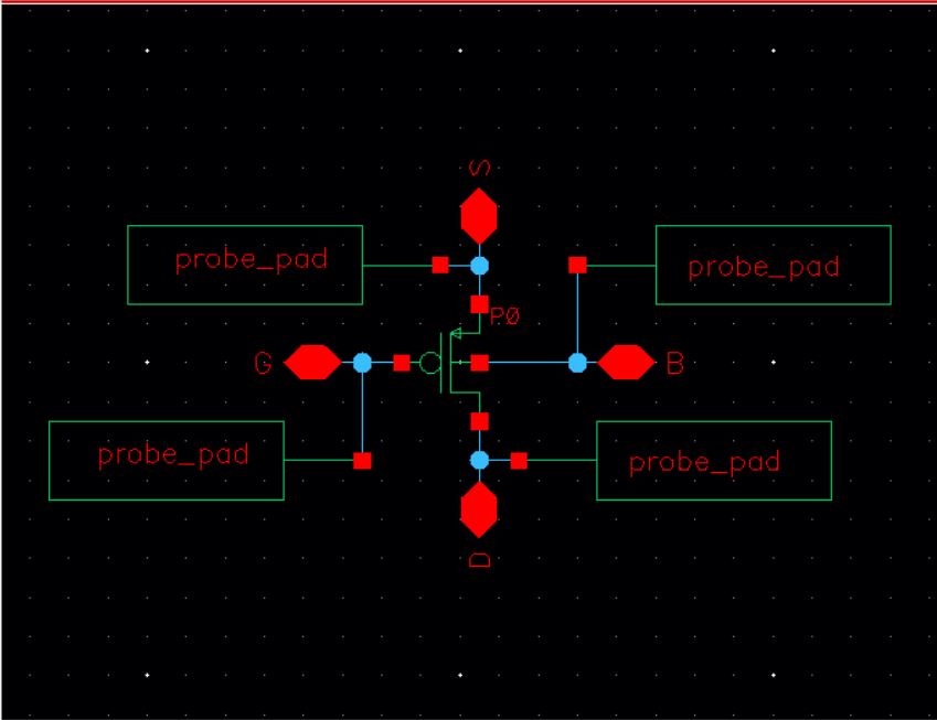
Once the layout has been made with the connected probe pads, we can connect the input/output pins made in the schematic:
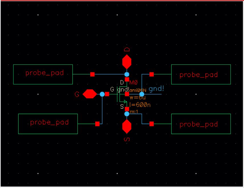
We can verify the model works by extracting the layout and comparing the schematic with the layout/extraction through an LVS:
Step 3: Lay out a 12u/0.6u PMOS device and connect all 4 MOSFET terminals to probe pads.
-> In the same fashion, since the PMOS was designed in the prelab, we can instantiate the PMOS device and connect probe pads.
-> Connect the new pins and DRC.
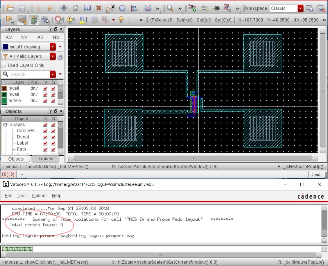
Since there were no DRC errors, we can then create the same layout with the schematic as:
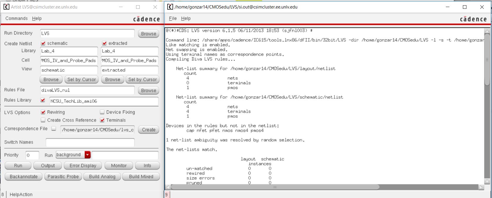
Then by extracting the layout, we can LVS the schematic and the layout as follows:
----------------------------------------------------------------------------------------------------
The design directory is downloaded from the MobaXterm server and backed up onto this website.
-> They are stored into my backup folder on my laptop and also on my online drive (as previously portrayed on the prelab).
----------------------------------------------------------------------------------------------------
This Concludes the Lab 4 Report.