Lab 03 - EE 421L
----------------------------------------------------------------------------------------------------
Prelab:
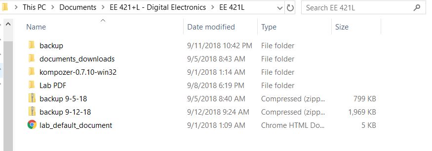
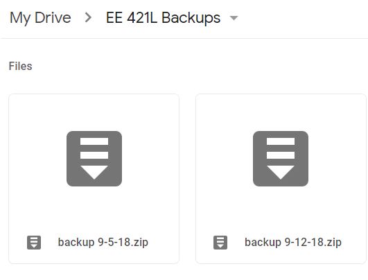
The labs are backed up through a saved directory in my computer as well as into my google drive account:
----------------------------------------------------------------------------------------------------
Lab:
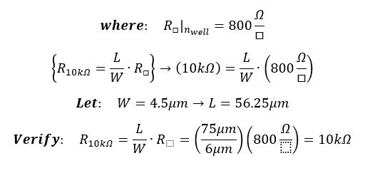
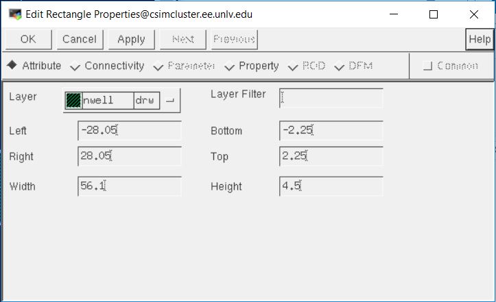
Step 1: Use the n-well to layout a 10k resistor as discussed in Tutorial 1.
-> Note that prior to creating the n-well resistor, we will adjust the dimensions to match the "ntap" layout file below.
-> In this case, the dimensions of the "n-tap" are a 3.6 x 4.5 microns.
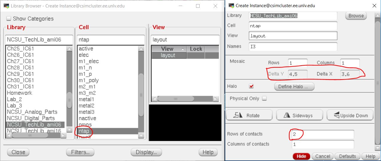
Therefore, when creating a '10k n-well resistor' rectangle into a new layout, the dimensions will be chosen as follows:
I created a library titled "Lab 3", then clicked "Create->Cell View->Layout".
In this layout, I will create a 10k n-well resistor using an "n-well" rectangle.
Note that the height is 4.5 microns like the ntap and the width is 56.1 microns to avoid DRC errors.
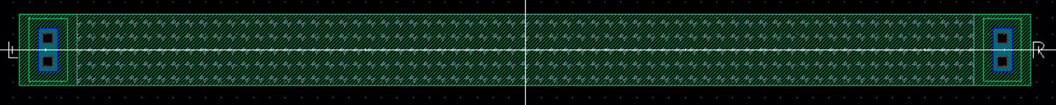
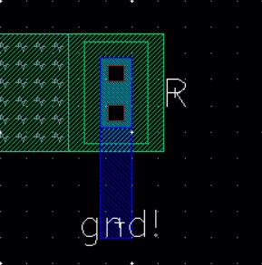
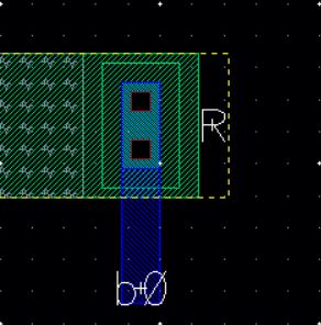
An "ntap" is added to each end of the resistor with metal1 pins connected to the "ntap" ends.
The pins are labled "L" for left and "R" for right. Lastly, a "res_id" is added over the n-well rectangle. The 10k n-well should look as follows:
Step 2: Use the n-well resistor in the layout of your DAC.
-> With the current n-well layout, we will save and "verify->DRC" to check for any errors.
-> We can also click "k" and use the ruler to verify the dimensions of the n-well as well (the ruler will be useful for the DAC layout).
-> This layout will then be extracted and used for the 10-bit DAC from Lab 2.
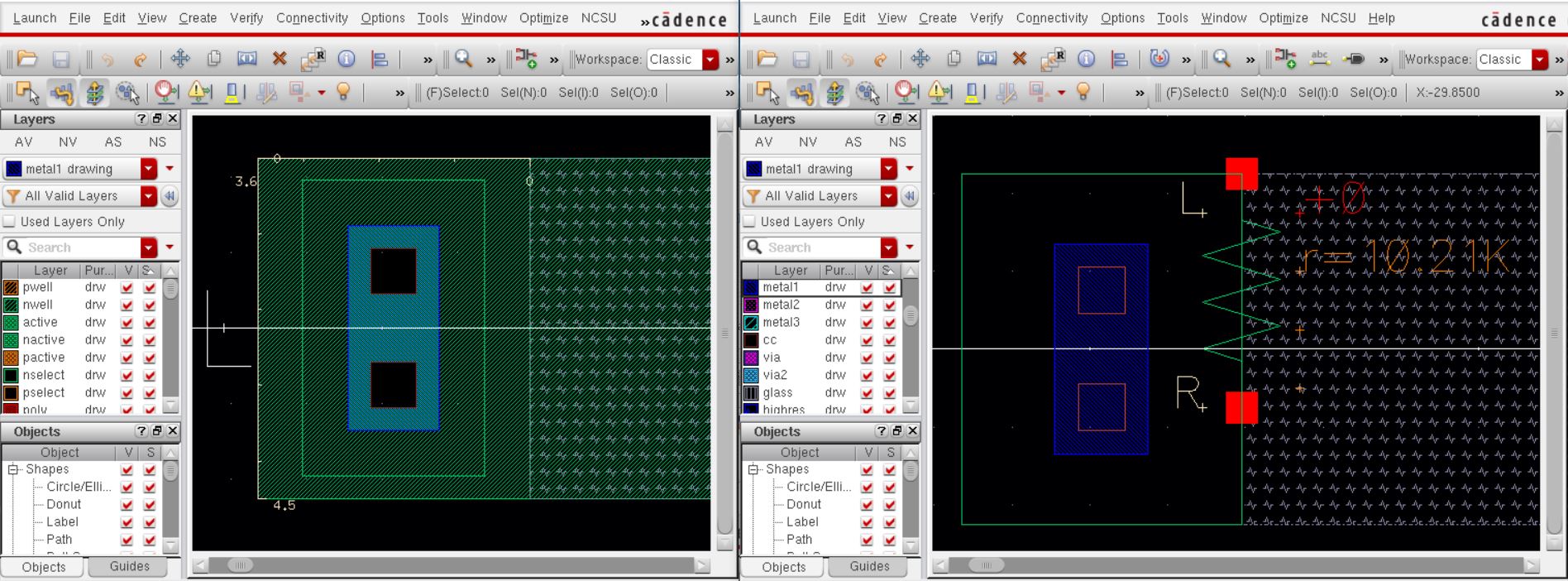
-> The layout and extracted file for the 10k n-well resistor should look as follows:
We can then close the current layout since it is no longer needed.
Instead we will copy the contents (schematic, symbol, etc.) from "Lab 2" and paste them into the "Lab 3" folder instead.
In the cell view of the "10-bit DAC", we will create a new layout that models the 10-bit DAC schematic.
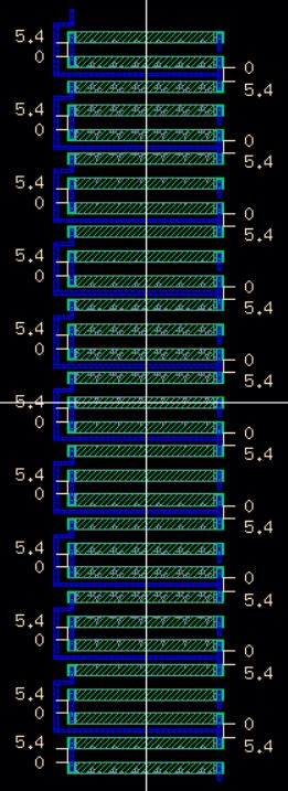
Step 3: Ensure that each resistor in the DAC is laid out in parallel having the same x-position, but varying y-positions (the resistors are stacked).
-> As previously mentioned, the ruler is a super handy tool to make measurements.
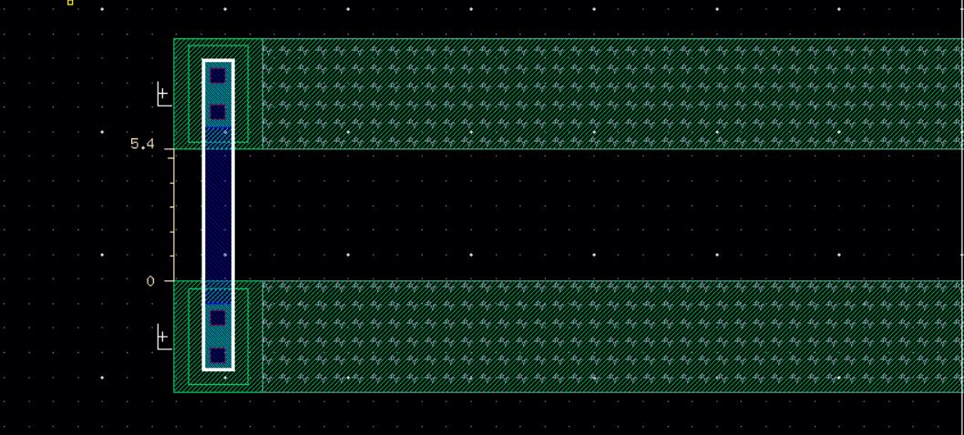
Since DRC requires that the distance between different n-wells be 5.4 microns apart,
we will utilize "k" (the ruler) to make sure each n-well is at least 5.4 microns apart then.
Since the 10-bit DAC is a tedious design, the following layout (2R||R) will be copied and pasted mutliple times to satisfy the 10 inputs.
With the below layout, we can easily add 9 more stacks and connect them with the help of using the ruler.
*Note that the 2R||R component has an open pin on the right side used for inputs later.
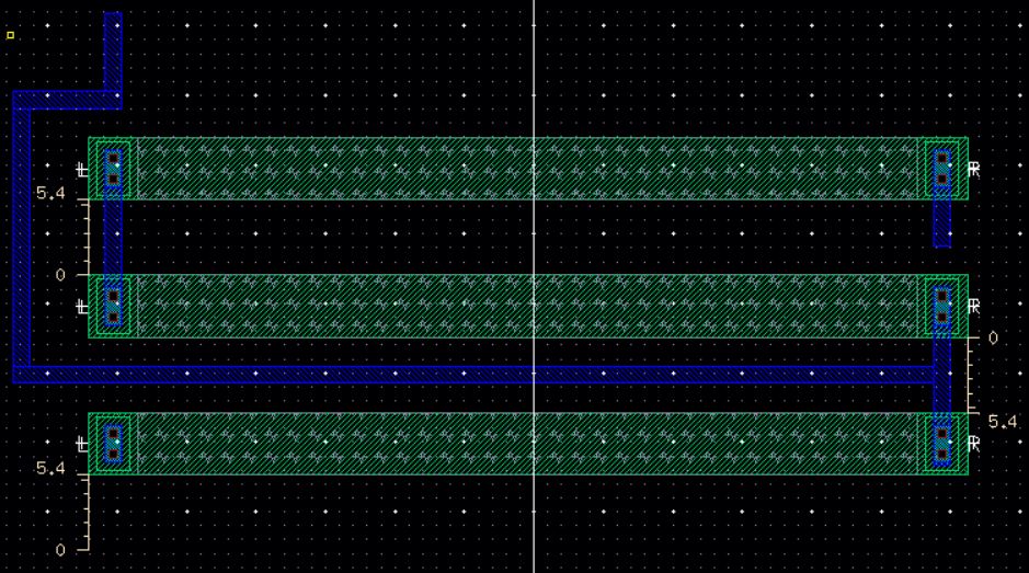
After connecting all 10 stacks, the bottom of the 10-bit DAC still needs 1 more n-well resistor.
The connected layout (and extracted view for step 5) should appear as follows:
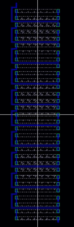
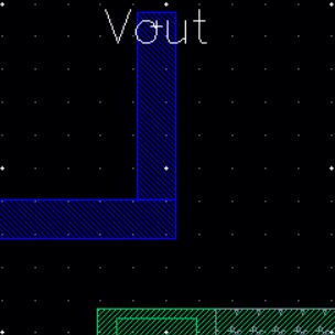
Step 4: All input and output Pins should be on metal 1.
-> Recall the right side of the 2R||R components have a metal1 end that can be connected to input pins.
-> Choose "Create->Pin" and connect pins accordingly: ground (gnd!), inputs (b0, b1,..., b9), output (Vout).
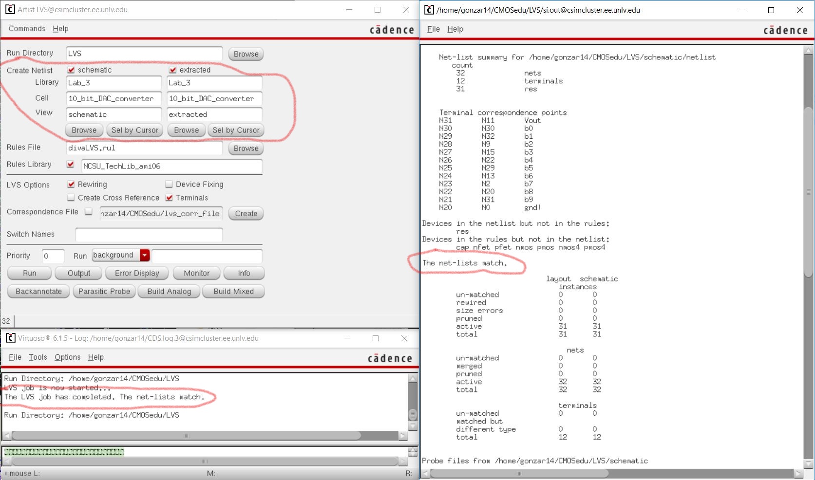
Step 5: DRC and LVS, with the extracted layout, your design (show the results in your lab report).
One of the last steps is to "Verify->DRC" which should show no errors:
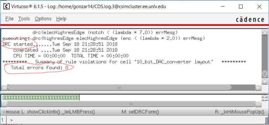
Then "Verify->Extract" and lastly "Verify->LVS" and match the schematic and extracted file together.
The pins should have the same names and pass without error. Once completed, the results will follow:
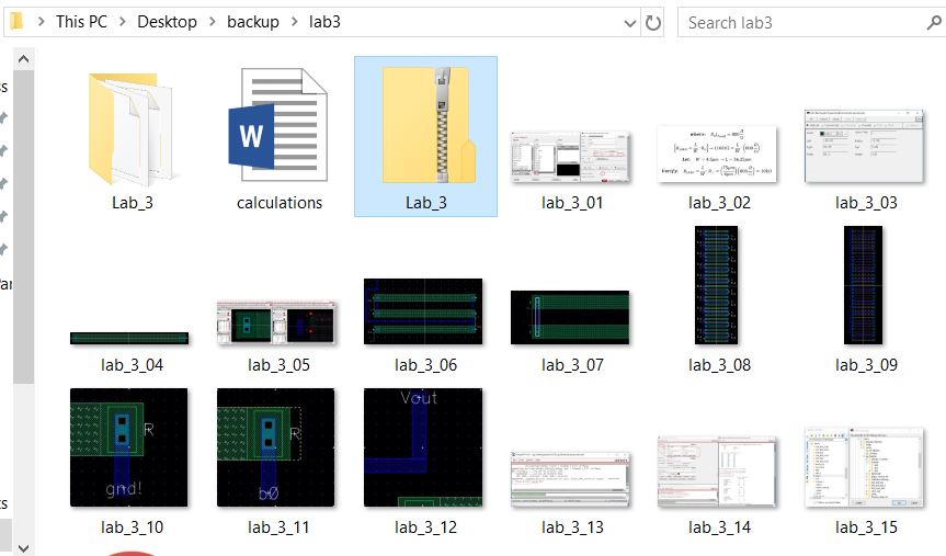
Step 6: Zip up your final design directory and place it in the lab3 directory, with a link on your lab report, so the grader can examine both the layout and schematic (and simulations).
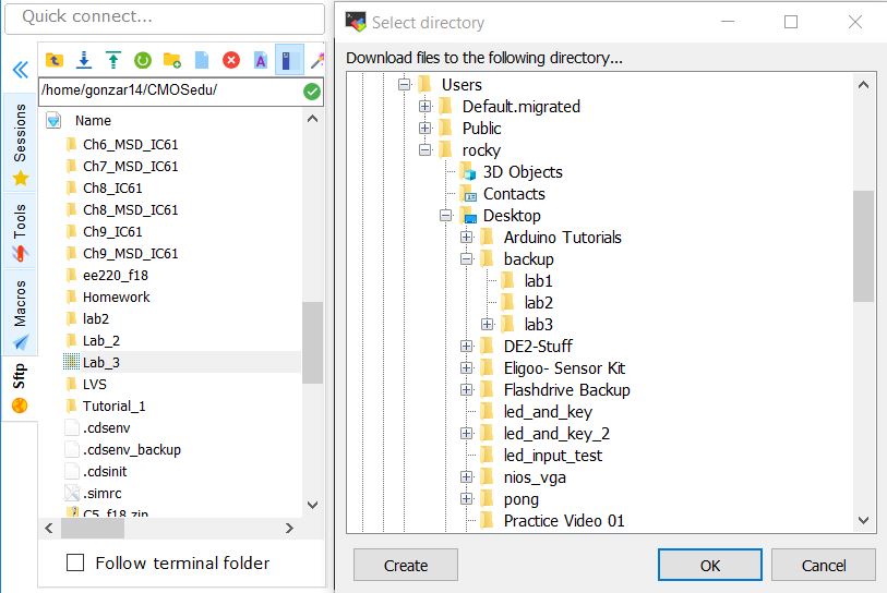
-> Through MobaXterm, I downloaded the folder "Lab_3" containing the contents of the project.
-> The file was zipped up can can be downloaded here.
----------------------------------------------------------------------------------------------------
This Concludes the Lab 3 Report.